石墨烯吸附氨气-2009
掺氮石墨烯的性质和应用
掺氮石墨烯的性质与应用1引言石墨烯是一种理想的二维材料,石墨烯中碳原子的sp2杂化结构使石墨烯具有理想的二维结构,它极大的比表面积(2630 m2/g)1,高热传导性(∼5000 W/mK)2,良好的化学稳定性以及较低成本等使它成为复合材料的理想载体。
目前已得到不同形态的石墨烯,包括二维结构的石墨纳米片(GNSs)3-5、一维结构的纳米条带(GNRs)、零维结构的量子点(GQDs)6,7,GNRs和GNDs的性质可以通过它们的大小和边缘进行调节。
然而,由于石墨烯没有能带间隙8,使得其电导性不能像传统的半导体一样完全被控制,而且石墨烯表面光滑且呈惰性,不利于与其他材料的复合,从而阻碍了石墨烯的应用。
对石墨烯进行功能化——合成石墨烯衍生物、表面官能团化、化学修饰、化学掺杂等,可以实现石墨烯及其相关材料更为广泛的应用9,10。
其中,化学掺杂能够有效地调节其电子结构,改善其物理化学性质,从而优化了石墨稀多方面的性能,具有广阔的应用前景。
由于N原子具有与C原子近似的原子半径,可以作为电子供体以取代的方式对石墨烯进行掺杂,且生成的N掺杂石墨稀表现出诸多优良的性能,如打开能带隙并调整导电类型,改变石墨烯的电子结构11,提高石墨烯的自由载流子密度12,从而提高石墨烯的导电性能和稳定性,增加石墨烯表面吸附金属粒子的活性位等。
在场效应晶体管、传感器、超级电容器、裡离子电池、燃料电池等领域的应用前景十分广阔。
因此,对石墨烯进行N掺杂这项课题,吸引着大批的科研工作者来探索。
通常有两种化学方法合成非金属掺杂石墨烯13-15,一种是取代掺杂,即令sp2构型的C被其它杂原子,如N、B、Si等取代。
另一种是在石墨烯表面吸附气体16,有机分子17或金属分子18实现功能化。
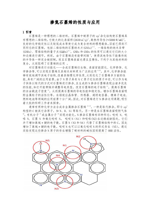
N掺杂石墨烯有四种形态:吡啶 N, 吡咯 N, 石墨 N 和氧化吡啶 N。
吡啶N(N1)和吡咯(N2)在边缘或缺陷处,它们并不增加离域π键的电子数。
石墨N(N3和N4)代替了石墨烯结构中的C,因此增加了离域π键的电子数。
石墨烯常用制备方法
石墨烯常用制备方法石墨烯是一种由碳原子构成的单层二维晶体结构,具有极高的导电性、热导率和机械强度,因此在电子学、光电子学、能源储存等领域具有广泛的应用前景。
本文将介绍石墨烯的常用制备方法。
1. 机械剥离法机械剥离法是最早被发现的石墨烯制备方法之一,也是最简单的方法之一。
该方法的原理是通过机械剥离的方式将石墨材料剥离成单层石墨烯。
具体操作方法是将石墨材料放置在硅基底上,然后用胶带反复粘贴和剥离,直到得到单层石墨烯。
这种方法的优点是简单易行,但是制备的石墨烯质量较差,且产量低。
2. 化学气相沉积法化学气相沉积法是一种通过化学反应在基底上生长石墨烯的方法。
该方法的原理是将石墨材料放置在高温下,使其分解成碳原子,然后在基底上沉积成石墨烯。
具体操作方法是将石墨材料放置在石英管中,然后将氢气和甲烷气体通入管中,使其在高温下反应生成石墨烯。
这种方法的优点是制备的石墨烯质量高,但是设备成本较高。
3. 化学还原法化学还原法是一种通过还原氧化石墨材料制备石墨烯的方法。
该方法的原理是将氧化石墨材料放置在还原剂中,使其还原成石墨烯。
具体操作方法是将氧化石墨材料放置在还原剂中,如氢气、氨气等,然后在高温下反应生成石墨烯。
这种方法的优点是制备的石墨烯质量高,且产量较高,但是还原剂的选择和操作条件对制备的石墨烯质量有很大影响。
4. 液相剥离法液相剥离法是一种通过液相剥离的方式制备石墨烯的方法。
该方法的原理是将石墨材料放置在液体中,然后通过超声波或机械剥离的方式将其剥离成单层石墨烯。
具体操作方法是将石墨材料放置在液体中,如水、有机溶剂等,然后通过超声波或机械剥离的方式将其剥离成单层石墨烯。
这种方法的优点是制备的石墨烯质量高,且操作简单,但是产量较低。
石墨烯的制备方法有很多种,每种方法都有其优缺点。
在实际应用中,需要根据具体需求选择合适的制备方法。
随着石墨烯制备技术的不断发展,相信未来石墨烯的制备方法会越来越多样化,也会越来越成熟。
石墨烯活性炭的作用和功效
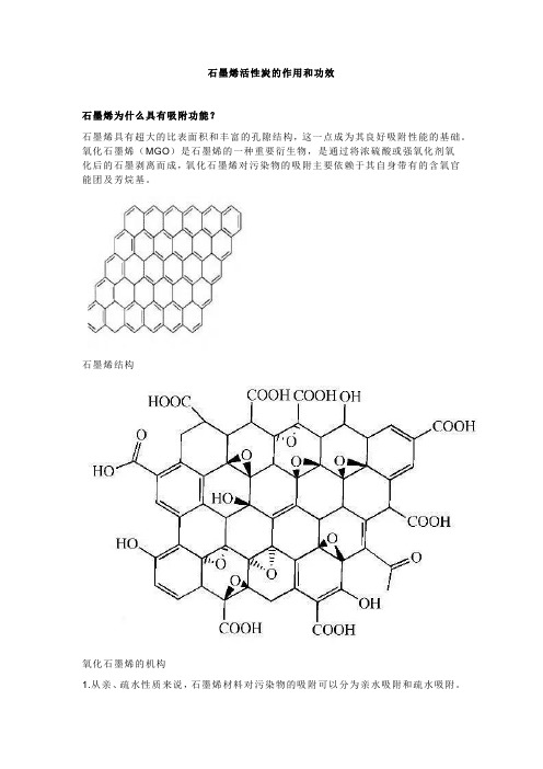
石墨烯活性炭的作用和功效石墨烯为什么具有吸附功能?石墨烯具有超大的比表面积和丰富的孔隙结构,这一点成为其良好吸附性能的基础。
氧化石墨烯(MGO)是石墨烯的一种重要衍生物,是通过将浓硫酸或强氧化剂氧化后的石墨剥离而成,氧化石墨烯对污染物的吸附主要依赖于其自身带有的含氧官能团及芳烷基。
石墨烯结构氧化石墨烯的机构1.从亲、疏水性质来说,石墨烯材料对污染物的吸附可以分为亲水吸附和疏水吸附。
氧化石墨烯的含氧官能团主要是“亲水基”更容易和亲水物质发生结合,易于同金属硫化物、金属原子、氧化物等结合形成氧化石墨烯插层复合材料,能够有效吸附去除水中多种有毒有害污染物;而芳烷基主要是“疏水基”更倾向于和疏水物质结合,能够有效吸附油污等污染物。
2.从理化性质来说,石墨烯材料对污染物的吸附可以分为物理吸附和化学吸附。
物理吸附:以分子间作用力为主的吸附,主要包括静电作用、π-π堆叠、疏水作用、氢键和范德华力作用,这几种吸附作用往往相伴产生。
化学吸附:以化学键为主的吸附,例如氧化石墨烯上的氧原子与金属离子发生的络合作用会促进吸附发生。
石墨烯能吸附哪些物质?研究表明,石墨烯及其复合材料可以吸附重金属离子,染料、抗生素、杀虫剂、原油等。
石墨烯及其复合材料吸附污染物一览表01吸附重金属离子重金属在水中大多以离子形式存在,其中以阳离子形式为主,如铜、锌、钴、镍、铅等,少部分以阴离子形式存在,如铬、砷等。
石墨烯材料处理重金属废水主要利用其比表面积大、吸附性能优异的特点,吸附去除重金属离子。
02吸附有毒气体吸附法被认为是一种最合理有效的治理空气污染的方法,石墨烯吸附气体分子主要依靠静电吸附作用、色散相互作用、范德华力以及电荷转移来实现。
我国科学家发明的“三维石墨烯基口罩”,能够有效去除(干、湿)空气中的粉尘及PM2.5,权威检测部门检测PM2.5过滤效率达99.6%。
另外,研究发现RGO/MnO2气凝胶对低浓度甲醛具有较好的去除能力,去除率达62.5%。
用氧化还原法制造石墨烯的方法
用氧化还原法制造石墨烯的方法
氧化还原法(即化学还原法)是一种常见的制备石墨烯的方法之一。
这个方法的基本思路是将氧化的石墨氧化物(如氧化石墨烯或氧化石墨烯烯)还原为石墨烯。
以下是一种基本的制备石墨烯的氧化还原法:
1.材料准备:首先,准备好氧化石墨烯。
通常,氧化石墨烯可以通过氧化石墨或氧化石墨烯烯的方法制备得到。
2.还原剂的选择:选择一种适当的还原剂,常用的还原剂包括氢气(H2)、氨气(NH3)、还原石墨烯氧化物的有机物(如乙醇、乙二醇)等。
3.还原反应:将氧化石墨烯与还原剂置于反应容器中,进行还原反应。
反应通常在适当的温度下进行,并可能需要一定的时间。
4.分离和纯化:完成还原反应后,需要对产物进行分离和纯化。
这包括对产物进行洗涤、离心、过滤等操作,以去除未反应的材料和副产物。
5.表征:对得到的石墨烯进行表征和分析,包括使用扫描电子显微镜(SEM)、透射电子显微镜(TEM)、拉曼光谱等技术来确定石墨烯的形态、结构和质量。
需要注意的是,氧化还原法制备石墨烯的具体操作条件和步骤可能会根据不同的研究目的和条件而有所不同。
此外,还有其他一些制备石墨烯的方法,如化学气相沉积法、化学剥离法等,每种方法都有其优缺点和适用范围。
石墨烯的吸附性能在环境保护中的应用
石墨烯的吸附性能在环境保护中的应用
石墨烯具有出色的吸附性能,被广泛应用于环境保护领域。
本文将重点介绍石墨烯在
水污染、空气污染和土壤污染等方面的应用。
石墨烯在水污染治理方面起到了重要的作用。
石墨烯具有高度的表面积和孔隙结构,
使其具有出色的吸附能力。
它可以吸附水中的重金属离子、有机物和微量有害物质,有效
净化水质。
石墨烯被广泛应用于废水处理中,可以高效吸附重金属离子,如铅、镉和铜等。
研究表明,石墨烯与金属离子之间通过静电作用和吸附作用结合,形成稳定的复合物,有
效去除了水中的有害物质。
石墨烯在空气污染治理中也发挥了重要的作用。
石墨烯具有优异的吸附和催化性能,
可以吸附和分解大气中的有害气体。
石墨烯基复合纳米材料被广泛研究,它能够吸附和降
解VOCs(挥发性有机化合物)和NOx(氮氧化物)等大气污染物。
石墨烯基光催化材料也
被用于净化有害气体。
石墨烯在光催化氧化反应中具有高光电化学转化效率,可以将有害
气体转化为无害物质,如二氧化碳和水。
石墨烯具有出色的吸附性能,在环境保护中的应用潜力巨大。
石墨烯在水污染治理、
空气污染治理和土壤污染修复等方面发挥着重要作用。
随着对石墨烯技术的进一步研究和
发展,相信石墨烯会在环境保护中起到更大的作用,为改善环境质量做出更大的贡献。
二维单质材料及其在气体传感器中的应用
36新技术·新业务·行业应用DOI:10.3969/j.issn.1006-6403.2024.03.009二维单质材料及其在气体传感器中的应用[吴家隐 刘志发 陈浩东 梁同乐 李先绪]二维材料具有了高载流子迁移率、电导率和热导率等优点,因此成为目前研究的热点。
近几年,随着石墨烯、磷烯、锑烯、碲烯以及锡烯等二维单质材料的兴起,越来越多的报道证明了二维单质材料用于气体传感的可行性与选择性探测的潜力。
二维单质材料可以降低敏感材料的维度,提高比表面积,进而极大的增加了气体传感器的灵敏度,能够在相对较低的温度下提供实时、在线的气体传感。
总结了近些年二维单质材料的最新研究进展,介绍二维单质材料的反应机理及其优势和特点,最后对该研究方向的发展进行了展望。
吴家隐广东邮电职业技术学院,副研究员,博士研究生,研究方向:物联网、传感器。
刘志发广东邮电职业技术学院,大专,研究领域:人工智能。
陈浩东广东邮电职业技术学院,大专,研究领域:人工智能。
梁同乐广东邮电职业技术学院,副教授,研究领域:云计算。
李先绪中国电信股份有限公司研究院,高级工程师,硕士。
关键词:二维单质材料 气体传感 石墨烯 磷烯 锑烯 碲烯 锡烯摘要1 引言随着工业化的推进和经济的发展,化石燃料大量消耗,污染物排放迅速增长,我国正面临越来越严峻的环境污染形势。
在环境污染物中,污染气体严重破坏生态环境,威胁着人们的身体健康。
主要大气污染物包括氨氮化合物、二氧化硫、氮氧化物、有机污染气体以及重金属等物质。
这些污染物的来源跟工业和生活息息相关。
在燃煤发电中,将产生大量的二氧化硫(SO 2)、氮氧化合物(NO x )、氯化氢(HCl )、重金属及其化合物以及气态有机污染物[1]。
其中,气态有机污染物主要包有易挥发性有机化合物(Very V olatile Organic Compounds ,VVOC )、挥发性有机化合基金项目:2022年广东省科技创新战略专项资金(大学生科技术创新培育)(pdjh2023b0915);2022年度广东省普通高校重点科研平台和科研项目特色创新项目(2022KTSCX289);2023年度广东省普通高校重点科研平台和科研项目新一代电子信息(半导体)重点领域专项(2023ZDZX1069);广东邮电职业技术学院质量工程项目(2023094、2023118、202201)。
石墨烯气敏材料的气敏性能研究
石墨烯气敏材料的气敏性能研究石墨烯作为一种新兴的二维材料,因其独特的结构和优异的性能引起了广泛的关注。
近年来,石墨烯在气敏材料领域的研究取得了显著的进展。
本文将探讨石墨烯气敏材料的气敏性能及其应用前景。
首先,我们来了解一下什么是气敏性能。
气敏性能是指物质对气体作用的变化特性,即物质对于不同气体在不同环境条件下的吸附、解吸、传输等过程的灵敏度和稳定性。
石墨烯作为一种具有高度结晶度和大比表面积的材料,具备了优异的气敏性能。
石墨烯的气敏性能主要体现在以下几个方面。
首先是其对于气体的选择性响应能力。
石墨烯能够响应多种气体,如氨气、一氧化碳、氧气等,并表现出很高的选择性。
这使得石墨烯可以应用于气体传感领域,对于环境监测、安全预警等具有重要的意义。
其次,石墨烯的气敏性能与其表面状态密切相关。
石墨烯的表面可以通过不同的方法进行修饰,如化学修饰、物理修饰等。
这些修饰可以改变石墨烯的气敏性能,使其对不同气体的响应能力发生变化。
例如,通过掺杂一些特定的元素,如氮、硫等,可以增强石墨烯对某些有毒气体的响应能力,提高传感器的灵敏度。
石墨烯的气敏性能还与其结构和尺寸有关。
石墨烯的结构可以通过调控其层数和形状来改变。
例如,多层石墨烯相比于单层石墨烯,表现出更高的气敏响应能力。
此外,还可以通过改变石墨烯的尺寸,如纳米片状石墨烯,来增强其气敏性能。
这些调控手段有助于提高石墨烯的气敏性能,并满足不同应用需求。
石墨烯气敏材料的研究不仅限于单一的性质表征,还包括了与其他材料的混合、复合等技术。
这些技术可以进一步提高石墨烯的气敏性能。
例如,将石墨烯与金属氧化物复合,可以显著提高传感器的灵敏度和选择性。
此外,还可以将石墨烯与纳米材料进行混合,以形成复合材料,从而扩展其应用范围。
石墨烯气敏材料的研究也涉及到其制备方法。
目前,石墨烯可以通过机械剥离、化学气相沉积等方法制备。
这些方法的选择会影响石墨烯的气敏性能。
例如,化学气相沉积法制备的石墨烯具有较高的结晶度和尺寸可控性,因此表现出更好的气敏性能。
掺氮石墨烯的制备及其ORR催化性能的研究
掺氮石墨烯的制备及其ORR催化性能的研究李鹏飞;王升高;孔垂雄;杜祖荣;邓泉荣;王戈明【摘要】Some outstanding properties of nitrogen-doped graphene has attracted much attention.The most synthesis methods of nitrogen-doped graphene need high temperature and long time which wiil destroy the structure of graphene and weaken the performance. In this article,we propose nitrogen plasma discharge method for synthesis of N-doped graphene sheets by simultaneous N-doping and reduction of graphene oxide(GO)sheets. Meantime,various characterization tech-niques,such as Raman,TEM are introduced. Electrical measurements demonstrate that products have higher catalytic per-formance for Oxygen Reduction Reaction in an alkaline solution.%由于掺氮石墨烯具有优异的电化学性能,受到研究者的关注,然而在石墨烯掺氮的方法中大部分(热解法、烧结法)需要过高的温度(500~900℃)和较长的反应时间(2~3 h)[1-3]。
采用微波等离子体对氧化石墨进行还原改性制备掺氮石墨烯,在低功率条件下反应时间只需20 min就得到了催化活性良好的掺氮石墨烯。
石墨烯氮化方法
石墨烯氮化方法石墨烯氮化方法简介石墨烯作为一种具有独特性质的二维材料,因其极高的导电性、热导率和机械强度而备受关注。
然而,石墨烯本身对氧气和湿气非常敏感,极易发生氧化和泛黄,导致其性质变化。
为了改善石墨烯的稳定性和功能性,氮化方法成为了一种重要的手段。
1. 氨气氮化法•简介:氨气氮化法是最常见的石墨烯氮化方法之一。
通过将石墨烯置于氨气环境中,使其与氮气发生反应,实现氮化目的。
•优点:简单易行,操作方便。
•缺点:氨气有一定的危险性,需要在安全条件下进行操作。
2. 氮离子注入法•简介:氮离子注入法是一种通过将氮离子注入到石墨烯中,实现氮化的方法。
•优点:可以实现对石墨烯的定向氮化,具有较高的氮化纯度。
•缺点:设备较为复杂,操作难度较大。
3. 氮化溶胶法•简介:氮化溶胶法是一种利用溶胶中的化学反应来实现石墨烯氮化的方法。
•优点:反应条件温和,能够实现较高的氮化度。
•缺点:溶胶制备和反应过程较为繁琐,需要一定的实验技巧。
4. 氧化石墨烯还原氮化法•简介:氧化石墨烯还原氮化法是一种将氧化石墨烯经过还原处理后进行氮化的方法。
•优点:能够充分利用已有的氧化石墨烯材料,节约资源。
•缺点:还原过程较为复杂,需要控制好还原反应的条件和时间。
结论石墨烯氮化方法具有多种选择,不同的方法适用于不同的研究需求和实验条件。
在选择合适的氮化方法时,需要考虑实验可行性、安全性和研究目的,综合评估后选择最适合的方法。
希望本文能够为石墨烯氮化研究提供一定的参考和指导。
1. 氨气氮化法氨气氮化法是目前最常见的石墨烯氮化方法之一。
这种方法的原理是将石墨烯材料置于氨气环境中,使其与氮气发生反应,实现氮化目的。
优点: - 简单易行,操作方便。
- 氨气易于得到,并且成本较低。
缺点: - 氨气具有一定的危险性,需要在安全条件下进行操作。
- 氮化度可能受到氨气浓度和氮气流量等因素的影响。
2. 氮离子注入法氮离子注入法是一种通过将氮离子注入到石墨烯中,实现氮化的方法。
石墨烯的研究进展
石墨烯的研究进展刘乐浩,李铁虎,赵廷凯,王大为(西北工业大学材料科学与工程学院,西安710072)摘要石墨烯是碳的又一同素异形体,具有独特的二维结构和优异的力学、电学、光学、热学等性能,成为富勒烯和碳纳米管之后的又一研究热点。
全面综述了近几年来石墨烯的制备方法,洋细讨论了微机械剥离法、化学剥离法、化学合成法、外延生长法、电弧法、化学气相沉积法的优缺点,并针对制备方法存在的产量低、结构不稳定、高污染等问题,提出了一些大规模可控制备高质量石墨烯的建议。
还结合石墨烯的结构和特性,概括了石墨烯在复合材料、微电子、光学、能源、生物医学等领域的应用进展,并展望了其主要研究方向和发展趋势。
关键词石墨烯制备方法应用中图分类号:〇613. 71 文献标识码:Research Progress on GrapheneLIU Lehao,LI Tiehu,ZHAO Tingkai,WANG Dawei (School of Materials Science and Engineering,Northwestern Polytechnical University,Xi,an 710072)Abstract As an allotrope of carbon,graphene has become a research hotspot due to its unique two-dimensional structure and excellent mechanical,electrical,optical and thermal properties. Synthesis of graphene via different approaches ,such as micro mechanical stripping, chemical stripping, chemical synthesis, epitaxial growth, arc dis- charge,and chemical vapor deposition, are discussed in detail, and strategies for producing homogeneous graphene with improved yield and structural stability while limiting its pollution are proposed. Also application progress of gre- phene in polymer composites,micro electronics, optics, energy and biomedicine are summarized, and the main research direction and development trend are imagined.Key words graphene,preparation methods,applicationo引言富勒烯[1]和碳纳米管[2]已经成为碳材料研究的热点,而在2004年,Geim等[3]又发现了碳的又一同素异形体——石墨烯(Graphene)。
- 1、下载文档前请自行甄别文档内容的完整性,平台不提供额外的编辑、内容补充、找答案等附加服务。
- 2、"仅部分预览"的文档,不可在线预览部分如存在完整性等问题,可反馈申请退款(可完整预览的文档不适用该条件!)。
- 3、如文档侵犯您的权益,请联系客服反馈,我们会尽快为您处理(人工客服工作时间:9:00-18:30)。
Home Search Collections Journals About Contact us My IOPscienceAdsorption of ammonia on grapheneThis article has been downloaded from IOPscience. Please scroll down to see the full text article.2009 Nanotechnology 20 245501(/0957-4484/20/24/245501)View the table of contents for this issue, or go to the journal homepage for moreDownload details:IP Address: 218.197.201.89The article was downloaded on 02/03/2012 at 03:40Please note that terms and conditions apply.IOP P UBLISHING N ANOTECHNOLOGY Nanotechnology20(2009)245501(8pp)doi:10.1088/0957-4484/20/24/245501Adsorption of ammonia on grapheneHugo E Romero1,Prasoon Joshi2,Awnish K Gupta1,Humberto R Gutierrez1,Milton W Cole1,3,Srinivas A Tadigadapa2,3,4and Peter C Eklund1,3,41Department of Physics,Pennsylvania State University,University Park,PA16802,USA2Department of Electrical Engineering,Pennsylvania State University,University Park,PA16802,USA3Materials Research Institute,Pennsylvania State University,University Park,PA16802,USAE-mail:sat10@ and pce3@Received26January2009,infinal form28April2009Published26May2009Online at /Nano/20/245501AbstractWe report on experimental studies of NH3adsorption/desorption on graphene surfaces.Thestudy employs bottom-gated graphenefield effect transistors supported on Si/SiO2substrates.Detection of NH3occurs through the shift of the source–drain resistance maximum(‘Diracpeak’)with the gate voltage.The observed shift of the Dirac peak toward negative gate voltagesin response to NH3exposure is consistent with a small charge transfer(f∼0.068±0.004electrons per molecule at pristine sites)from NH3to graphene.The desorption kinetics involvesa very rapid loss of NH3from the top surface and a much slower removal from the bottomsurface at the interface with the SiO2that we identify with a Fickian diffusion process.(Somefigures in this article are in colour only in the electronic version)1.IntroductionGraphene is a singleflat atomic sheet of carbon with the atoms arranged in a two-dimensional(2D)honeycomb configuration.Recent progress in isolating graphene on an insulating substrate(e.g.,SiO2or SiC)now enable this exotic 2D system to be probed experimentally[1–3].It has been shown to be a promising building block for novel generation of high speed and sensitive electronic devices[4–12].Electron transport experiments on graphene have demonstrated,among other effects,unusual carrier-density-dependent conductiv-ity[1,13,14],anomalous quantum Hall effect[13–15], minimum quantum conductivity[13],and exceptionally high electron mobilities[16,17].These remarkable electronic properties stem from the unique band structure of graphene, which exhibits conduction and valence bands with near-linear dispersion that touch at the Brillouin zone corners to make a zero gap semiconductor.Similar to earlier experiments on carbon nanotubes[18], the transport properties of graphene have been shown to be sensitive to molecules adsorbed on the surface(e.g.NH3,NO2, H2O and CO)[10,19].The details of the strength and character of the adsorption(chemi versus physisorption),and the degree of charge transfer between the analyte and graphene is still 4Authors to whom any correspondence should be addressed.under debate.Geim and co-workers were thefirst to report that a graphene Hall effect sensor device is capable of detecting individual molecules of NO2[10].Charge transfer between the graphene and NO2is thought to be important in this particular case[19,20].Here,we report studies of the interaction of NH3with graphenefield effect transistors(FETs)supported on Si/SiO2 substrates in order to provide further insight into the nature of the molecule–graphene interaction.The SiO2is used as a gate dielectric and the heavily doped Si substrate as the bottom gate electrode.By sweeping the gate voltage,we can follow the time evolution of the peak in the drain-source resistance (known as the‘Dirac’peak)to monitor the change of the Fermi level in graphene in response to the adsorption and desorption of NH3.Presumably,this shift of the Dirac peak is dominated by charge transfer effects.The Dirac peak shift and the thermodynamic data for NH3on graphite are used to determine the effective charge transfer per NH3molecule(f) to the graphene.Our value for f will be compared to recent theoretical calculations for NH3bound to the surface[20]and to the edges[21]of graphene.2.Experimental detailsThe graphene FETs studied here were supported on Si/SiO2 substrates and bottom-gated using the SiO2(300nm thermalb)10m μ10οmI II IIIII(a)(b)IIIII III 210 μm Figure 1.(a)Schematic of a graphene device supported on SiO 2with underlying doped Si serving as the back gate (G);S and D refer to thesource and drain contacts.(b)Optical micrograph of a graphene device fabricated with TEM grids as a shadow mask.The graphene flake is ∼3μm wide in this device.The following areas can be identified on the optical image:(I)single graphene layer (also indicated with dashed lines),(II)Cr/Au electrodes,and (III)SiO 2dielectric.oxide)as the gate dielectric and the degenerately p +doped Si substrate (ρ∼3×10⁻³ cm)as the gate electrode.Our graphene films were produced by mechanical exfoliation of highly oriented pyrolytic graphite (HOPG Grade ZYH TM ,SPI Supplies,Inc.,West Chester,PA)using adhesive tape (Scotch Tape,3M,Inc.,Maplewood,MN).Before the transfer of graphene flakes,the Si/SiO 2substrates were first cleaned in isopropanol and later exposed to O 2-plasma.The FET was constructed by the physical vapor deposition of pads of Cr(5nm)followed by Au(100nm)for electrical contact at opposite ends of the graphene FET channel (i.e.,the ‘source’and ‘drain’).The Cr and Au were evaporated onto the graphene through square holes in a transmission electron microscopy (TEM)grid (SPI Supplies,Inc.,West Chester,PA)used as a shadow mask and consisted of a 10×10array of 115×115μm 2square holes separated by ∼10μm bars.By using a micromanipulator while viewing the area through an optical microscope,the TEM grid was carefully positioned on the graphene flake of interest (i.e.,natural flakes of approximately rectangular shape and more than 10μm long)so that one the TEM bars covers the graphene along its width,leaving its ends uncovered through the apertures of the mask.Then,the TEM grid is temporarily clamped to the substrate during contact evaporation.Our approach for fabricating electrical contacts avoids unnecessary complications that may stem from the exposure of the graphene to lithography chemicals.A schematic drawing of our bottom-gated field FET that is supported on a Si/SiO 2substrate is shown in figure 1together with an optical micrograph of the device.The optical image in figure 1shows a particular FET with two square Cr/Au contacts deposited over each end of a rectangular graphene flake.The number of layers (N )in a graphene film was determined by micro-Raman scattering using the shape of the 2D Raman band at ∼2700cm −1and the intensity of the Raman-active G-band scattering at ∼1585cm −1[22,23].The Raman characterization of N can be summarized as follows:[22](1)the G-band intensity is approximately linear in N ,(2)an N =1graphene film can be easily recognizedby the narrow Lorentzian shape of the 2D Raman band,(3)at least one N =1film must be present on the same substrate so that the relative G-band intensity associated with other films can be measured by a simple translation of the microscope stage while all optics remain fixed.Here,we present results on one representative sample that was demonstrated by Raman scattering to be a N =1graphene film of dimensions ∼10μm ×1.5μm.Each Si/SiO 2substrate supporting several graphene FETs was mounted on a ceramic chip carrier that was placed in a socket fixed inside a vacuum sealed stainless steel (SS)tube equipped with vacuum and gas (NH 3)connections.The SS tube was inserted into a tube furnace and evacuated to 5×10⁻⁷Torr using a turbo-molecular pump.Vacuum-annealing of the samples were performed in situ by heating to 200◦C at a constant rate of 2◦C min −1to drive out all gases.Once the vacuum-annealing procedure was ceased and graphene reached a fully degassed state,the samples were allowed to cool to room temperature.We assume that graphene is a fully degassed state when there is no further evolution of the Dirac peak shape and/or position with time at 200◦C.Samples could then be exposed to anhydrous NH 3(99.99%,H 2O <1ppm)diluted in ultra high purity He (99.999%).A type-K thermocouple was mounted on the chip carrier near the Si substrate to monitor the local temperature.Electrical measurements were made using a programmable voltage source and digital voltmeter/ammeter (2400General-Purpose SourceMeter,Keithley Instruments,Inc.,Cleveland,OH)interfaced to a computer via LabVIEW (National Instruments Co.,Austin,TX).The measurements consisted of the application of a constant source–drain voltage V ds =1mV to the device,while monitoring the resultant source–drain current (I ds )as a function of the applied gate bias (V g ).The source–drain resistance was computed as R ds =V ds /I ds .3.Results and discussionSince our device fabrication scheme involves shadow masking to make contacts to graphene films,it therefore has the-33530252015105(b)R ds )t (h )V g (V )(a)(k Ωrs )t (hours)V D i r a c (V )906030Figure 2.Time evolution of (a)the R ds versus V g curves at T =200◦C during the first 8h of vacuum-annealing of the graphene FET device shown schematically in figure 1.Initially,the Dirac peak is out of range (V g >90V);after ∼5h,the Dirac peak appears at negative V g and evolves slowly to the final position at V g ∼−47V .This particular sample was vacuum annealed for ∼72h,when the position of V Dirac stop evolving with time,i.e.,sample reached a saturation;(b)the gate voltage for the charge neutrality point,V Dirac ,during vacuum-annealing of a graphene FET at T ∼200◦C.advantage that it is a lithography-free process.Recent studies have shown that resist,such as poly(methyl methacrylate)resin,can be quite difficult to remove,requiring heat treatment at 400◦C in Ar/H 2flow [24].These adsorbed molecules may dope (i.e.,charge transfer with)the sample,or may block active adsorption sites for analytes and/or might otherwise interfere with the reproducibility of the FET electrical data.The electronic band structure of graphene near the Fermi level (E F )is somewhat unique.Near-mirror image valence and conduction bands touch each other at the six corners (K,K points)of a 2D Brillouin zone.These contact points are commonly called ‘Dirac points’[1].This nomenclature stems from the linear dispersion of the electronic energy (E )with 2D wavevector (k ),i.e.,E =±¯h v F k ,where v F is the Fermi velocity of the electrons.In pristine graphene,E F is located where the conduction and valence bands touch,i.e.,the Dirac point.A FET built from pristine graphene (i.e.,where E F is located near the Dirac point)should exhibit ambipolar conduction.That is,depending on the sign of the gate bias voltage (V g ),the gate induces E F to rise or fall in the band structure and as a result either electrons or holes dominate the source–drain current (I ds ).Defining the source–drain resistance as R ds =V ds /I ds ,where V ds is the applied potential difference between source and drain,it can easily be shown that the position (V Dirac )of the peak in R ds is related to n ,the 2D net carrier density [1].Thus,the ambipolar character of graphene FETs refers to the fact that V g can be used to control n (gate-induced doping).A transition between electron and hole conduction can be shown to occur when V g positions E F at the Dirac point (n =0),where the conduction and valence bands touch.Since this is the position in ‘intrinsic graphene’,this value of V g also achieves charge neutrality in the graphene.An approximate relationship between n (in number of electrons cm −2)and V g can be used to describethe device response to gate voltage [1],n ≈εε0(V g −V Dirac )/le ≡α(V g −V Dirac )(1)where εε0and l are,respectively,the gate dielectric permittivity and thickness,e is the charge of the electron and V Dirac is a constant.Equation (1)is an approximate relationship,in that thermal broadening of the Fermi–Dirac function is not included.Using the well known linear electronic π-band dispersion,it is easy to show that the carrier concentration (electrons orholes)∼E 2F [25].The accepted value for the Fermi velocity is v F ∼c /300,where c is the speed of light [13,14].Using equation (1),and the values l =300nm,and ε/ε0∼3.9,we can therefore obtain an approximate numerical relationship between E F and V Dirac for our graphene FETs,i.e.,E F ≈±31.7(meV /√V )V Dirac (2)where the positive and negative signs apply,respectively,to hole and electron conduction.This equation,however,ignores the details of the electrostatics in the FET and the SiO 2/graphene interface.When these details are included,the left (or right?)side of equation (1)contains an additional small term that is proportional to √n [25].Our graphene FETs were exposed to ambient conditions for several days before electrical characterization.We found that most of our devices exhibited a Dirac peak in the range +50V <V g <+100V ,i.e.,they are p-type.A positive shift of the Dirac peak of the same order of magnitude is not uncommon in graphene devices on Si/SiO 2substrates [1,26,27].However,all our samples’p-doping can be reversed by vacuum-annealing at 200◦C and ∼5×10⁻⁷Torr over ∼10–200h.Over this time,the peak passes through V g =0V and ends up in the range −10V <V g <−60V ,depending on the sample (cf figure 2).We have interpretedR d s (k Ω)-9-44321t (m in )V g (V)(a)t (min)5t (hours)V D i r a c (V )Figure 3.(a)Response of bottom-gated graphene FET (on Si/SiO 2)to a sudden overpressure of 1atm of 10%NH 3in He during the first exposure.The initial Dirac peak corresponds to the FET before NH 3exposure.Data were collected in the range −90V <V g <+90V to avoid breakdown of the gate dielectric.(b)Time dependence of the Dirac voltage V Dirac ,during NH 3desorption at T =25◦C,after two successive exposure–desorption cycles (1)and (2).The solid lines are fit of the data to a double exponential function.these results [25],to indicate that the p-doping occurs from ambient exposure to air and stems from the adsorption of O 2molecules that remove electrons from the graphene.A clean graphene sample supported on Si/SiO 2should be n-type [25].This conclusion stems from work function (W )calculations [25]for graphene and amorphous Si where we found that W (SiO 2)is ∼1eV higher than in graphene,as E F in SiO 2is pinned in a surface state band located just below the conduction band edge.In the present studies of the response of graphene FETs to NH 3,we start with the graphene FET in a fully degassed state,i.e.,it is initially n-type.We now discuss the time response of our n-type FETs to a sudden rise in NH 3pressure.We present all data from one device,but the same general behavior was observed in six devices.As described above,the typical device chosen for analysis here was first degassed in high vacuum at 200◦C for ∼72h until the Dirac peak remained fixed at a negative gate bias V g ∼−47V .The particular device for systematic study was then cooled in vacuum to T =25◦C and exposed for 30min to 1atm overpressure of 10%NH 3gas diluted in He.The time evolution of Dirac peak to this first NH 3exposure is shown in figure 3(a).The Dirac peak can be seen to shift rapidly to more negative V g ,eventually moving beyond the safe gate voltage limit for our FETs,i.e.,V g ∼−90V .The shift of the Dirac peak to more negative V g shows clearly that NH 3appears to be acting as an n-type dopant,upshifting the position of E F in the electron pockets at the Brillouin zone corners.All six graphene FETs showed this rapid shift of the Dirac peak to negative V g beyond our safe gate limit.Indeed,the electrical response to NH 3at T =25◦C is so rapid that we propose that it is determined by either adsorption onto the top surface of the graphene,or by top surface chemical reactions whereby the NH 3displaces strongly bound molecules remaining after degassing.We expect therefore that the diffusion of NH 3into the SiO 2/graphene interface is a much slower process.Next,the NH 3-dosed FET wasexposed to vacuum desorption conditions,i.e.,the NH 3supply is isolated and the sample chamber was rapidly evacuated in ∼10s,i.e.,the NH 3overpressure therefore drops very rapidly compared to the characteristic time for the ensuing changes in the FET resistance.The kinetics for the first desorption cycle at T =25◦C can only be followed once the Dirac peak recovers below our gate voltage limit of V g =−90V .As can be seen in the figure,the desorption kinetics at T =25◦C are considerably slower than estimated for the adsorption response (figure 3(b),curve 1);we observed that this particular device recovers during desorption from being very strongly n-type (i.e.,when the Dirac peak appears at gate voltages beyond −90V)to exhibit a new stationary value V Dirac ∼−52V in ∼5h which is somewhat more negative than the initial vacuum-degassed FET state (V Dirac =−47V).Each N =1device behaves a little differently in the details of the kinetics and final equilibrium values of the Dirac peak.The NH 3response of this particular device is typical of the general character of all devices measured.Next,the FET was further degassed in vacuum at T =100◦C until R ds (V g )no longer changed with time,after which it was cooled down to room temperature,and exposed to the same 10%NH 3/He mixture at p =1atm a second time.The Dirac peak was then observed to rapidly shift again toward more negative V g ,disappearing behind our (device-safe)gate dielectric limit of −90V .As can be seen in figure 3(b),the device response to a second desorption (degas)cycle (curve 2)at T =25◦C is similar to the first desorption (degas)cycle (curve 1).Curve 2shows the Dirac peak rapidly upshifting from below −90V to a new steady state value of −38V at T =25◦C in vacuum which is less negative than was observed after the first cycle.The solid lines in figure 3(b)represent fits to the desorption data by a double exponential function,V Dirac (t )=V ∞+V 1exp (−t /τ1)+V 2exp (−t /τ2)(3)where t is the time and τ1and τ2are effective time constants.The constant V ∞in equation (3)is the steady state position40302010V g (V)40302040302010R d s (k Ω)Figure 4.Room temperature source–drain resistance as a function of gate voltage for three successive NH 3exposure–desorption cycles (1)–(3).Three representative R ds (V g )curves are plotted:before NH 3exposure (solid lines),after NH 3desorption at T =25◦C (dotted lines),and after vacuum-degassing at T =100◦C (dashed lines).The arrows indicate the position of the Dirac peaks.of the Dirac peak after long-term desorption.As can be seen from the figure,equation (3)provides a good description of the experimental observation.Of course,for the double exponential fit to be meaningful,we expect to obtain two very different values for τ1and τ2.Indeed,the slow and fast components of the NH 3desorption process are (first desorption)τ1=2.1±0.2h and τ2=0.22±0.02h (i.e.,τ1/τ2=9±2);(second desorption)τ1=30±1min and τ2=4±1min (i.e.,τ1/τ2=8±3).The values returned for the prefactors are,respectively,(first desorption)V 1=−18.3±0.4V and V 2=−12.1±0.7V ,(second desorption)V 1=−30.2±0.8V and V 2=−13.5±0.5V .Our results indicate that the FET desorbs somewhat faster the second time.We are not sure what the physical or chemical implications are for this change in response times.The fact that the ratio τ1/τ2∼9is found to be the same for both desorption cycles is discussed below and appears to stem from Fickian diffusion.All samples showed the general behavior exhibited by V Dirac (t )with the kinetics described by a combination of fast and slow processes (equation (3)).In one other sample,we did a fitting of equation (3)to the data and again found the ratio τ1/τ2=9.5±0.6.In figure 4,we show the representative R ds (V g )curves corresponding to the first (bottom,curves 1),second (middle,curves 2),and third (top,curves 3)NH 3exposure–desorption cycles.The Dirac peaks are coded in the figure to indicate when they were collected:before NH 3exposure (solid curve),after NH 3desorption at T =25◦C (dotted curve)and after NH 3desorption at T =100◦C for ∼16h in vacuum (dashed curve).As shown in figure 4,the amplitude andposition of the Dirac peak were not observed to recover exactly to their original vacuum-degassed FET state values after a T =25◦C vacuum desorption.However,after a T =100◦C vacuum desorption,the amplitude,but not the position,of the Dirac peak recovers to the original (degassed state)value;the Dirac peak shift appears at a slightly less negative V g value after this treatment.We attribute this result to the possibility of displacement chemical reactions in the SiO 2/graphene interface whereby the NH 3molecules displace some species that weakly charge transfer,thereby partially neutralizing the ambient p-doped SiO 2surface.Despite much effort by several groups,the interaction of NH 3with SWNTs remains controversial.A few years ago,it was reported that individual semiconducting nanotubes (s-SWNTs)could be used to detect small concentrations of NH 3with high sensitivity by measuring changes of the nanotube conductance and the FET threshold voltage [18].The authors reported that the electrical conductance of a p-doped nanotube-FET decreased by approximately two orders of magnitude after exposure to a flow of 1%NH 3at room temperature,and they suggested that a charge transfer of electrons from NH 3to SWNTs was responsible for the change in properties of the SWNTs.On the other hand,theoretical calculations on isolated defect-free nanotubes predicted that NH 3molecules should physisorb to the tube wall without significant change of the band structure,although a very small charge transfer of f ∼0.03−0.04e per adsorbed NH 3molecule was predicted to occur [18,28–31].Therefore,from this work on SWNTs it appears that experimental and theoretical results are consistent with the NH 3acting as a weak n-type dopant,overriding or compensating the initial p-type behavior deduced from the sign of the gate voltage at threshold.Theoretical studies of gas adsorption on a pristine graphene surface have also been reported recently by that indicate that NH 3molecules can act as donors with a small charge transfer of f ∼0.03e [20].This is consistent with calculations on defect-free SWNTs [18,28–31].More recent theoretical investigations have explored the adsorption of NH 3on nanotubes near wall defects,e.g.,Stone-Wales defects [32].The results are possibly relevant to our study in graphene and can be summarized as follows:(i)chemisorption of NH 3at a wall defect is an exothermic process with a relatively low activation barrier;therefore chemisorption of NH 3near these defects should readily happen at room temperature;(ii)NH 3adsorption at defects is accompanied by a high charge transfer,i.e.,f =0.18e ;(iii)the presence of pre-dissociated oxygen near or at the defect enhances the NH 3chemisorption process which becomes nearly spontaneous.These significant electron transfers from chemisorbed NH 3at defects,rather than low charge transfer at more numerous pristine sites might also explain the large drops in electrical conductance of s-SWNTs observed experimentally [18,33].It is also relevant to our results here that recent temperature-programed-desorption (TPD)measurements of NH 3on SWNTs indicate that NH 3can be strongly bound to the SWNT surface (i.e.,chemisorbed)[34].Perhaps this conclusion is consistent with a weak charge transfer that enhances the binding energy of the NH 3to the tubewall,i.e.,over and above that associated with physisorption.In these TPD experiments,most of the NH 3gas desorbed only at elevated temperatures (500–700K).In addition,and in contrast to the previous work on NH 3-SWNTs,Bradley et al [35]found that vacuum-degassed nanotube-FETs were insensitive to NH 3.They suggested that for NH 3gas to be detected in the FET response,the NH 3must first dissolve in a H 2O monolayer which forms on the nanotube-FETs under ambient lab conditions.They proposed that the NH 3molecule in this environment can become a cation with the charge being compensated in the SWNTs,i.e.,act as an n-dopant.As a result,it was proposed that the nanotube-FETs respond to NH 3gas only when they are exposed in ambient (humid)conditions.Feng et al [32],on the other hand,reported experimental evidence of the extreme sensitivity of NH 3adsorption on thermal-annealing prehistory.Their results revealed a systematic decrease of NH 3adsorption on SWNTs after they were annealed to successively higher temperatures from 500up to 1400K.However,they did not identify the decrease in NH 3doping on a reduction in H 2O bound to the surface,but rather to large charge transfer associated with less numerous sites near functional groups (e.g.,chemisorbed O 2)and defects on the surface that can be removed by vacuum-annealing.Upon exposure of our degassed graphene FET to 0.1atm of NH 3,the Dirac peak rapidly shifted past our safe gate voltage limit and we were therefore only able to partially observe the R ds (V g )peak,i.e.,the peak itself and its negative voltage tail were beyond the gate limit.Since we did not observe any significant change in the shape of the R ds (V g )curves as they shift with adsorption/desorption,we then fit this partial R ds (V g )curve to obtain the peak position,i.e.,V Dirac ∼−140V .Before NH 3exposure,the degassed device exhibited a Dirac peak at −47V;we therefore observed a negative shift in the Dirac peak of V Dirac ∼90V due to equilibrium adsorption of NH 3under our experimental conditions.The same basic behavior was observed in five other graphene FETs.The shift V Dirac was detectable in three other samples where the tail of the Dirac peak was still visible within our gate voltage limit,as described above.The estimated values of V Dirac determined as described above by a rigid shift of a typical Dirac peak,are 100V ,89V ,and 90V ,respectively.In average, V Dirac =92±5V .We can interpret the ∼92V Dirac peak shift due to equilibrium coverage of NH 3under our experimental conditions in terms of the charge transfer of electrons between adsorbed NH 3and the graphene.For simplicity,we can begin to analyze this process by assuming a monolayer coverage of NH 3in a closed-packed hexagonal configuration [36],anduse the collision diameter for NH 3,i.e.,d ∼4.09˚Afor the effective molecular diameter [37].The effective graphene area per NH 3molecule is therefore A m =√3(√3+1)2d 2/14.The relationship between the charge transfer per molecule f ,A m and the excess charge per unit area on the graphene ( n )is given by f = n A m ,which by equation (1)can be expressed as f =α V Dirac A m .Using this equation,we can estimate f ∼0.01e for a monolayer coverage of NH 3on graphene.This value of f is approximately a factor of 3lower than that predicted by theory [20].However,based on thermodynamic data for NH 3on graphite [38,39],a surface coverage of much less than a monolayer is expected.Our estimate for f must be refined to take this lower coverage into account.The well known thermodynamic relationship between surface coverage and binding energy E b is given by [40]ρsurface =ρgas exp E bk B T (4)where ρsurface and ρgas are,respectively,the three-dimensional (3D)number density on the surface and in the gas phase.This relationship is derived assuming that only one molecule can occupy a site with this binding energy and there is no interaction among the adsorbed molecules.The fractional coverage is defined as θ=A m d ρsurface .Using the experimental thermodynamic value E b =0.18eV [38,39],we find θ=0.15for p =0.1atm (partial pressure of NH 3)and T =25◦C which is indeed much less than a monolayer.We then correct our estimation of the charge transfer f taking into account the fractional coverage θ=0.15.With this coverage we obtain f ∼0.068±0.004electrons per NH 3molecule.This value is in excellent agreement with the recent theoretical study of the physisorption of NH 3on defect-free graphene discussed above [20].It is important to notice that since our graphene was fully degassed in vacuum at 200◦C for long periods of time,we do not expect any significant interference from H 2O and/or O 2on the surface,as discussed above in relationship to Bradley et al ’s work with NH 3on s-SWNT FETs [35].To make sure the NH 3gas (stated to be <1ppm H 2O)did not bring significant H 2O into our experimental chamber,we carried out one additional experiment first introducing a KOH trap between the gas cylinder and the chamber.Essentially the same experimental results were obtained.Similar to SWNTs,recent theoretical calculations [21]showed that NH 3can strongly adsorb on defect sites located at a graphene’s edge and significantly influence the electronic and transport properties of narrow ribbons.The charge transfer at these edge sites is high,f =0.27e [21].Consequently,it is important to consider the possibility that defect sites might affect NH 3detection by graphene ing equation (1),we can write f =α V Dirac w/2λ,where w =1.5μm isthe average width of our graphene flake and λ=0.47˚A−1is the defect concentration on a graphene flake having two free armchair-shaped edges.Assuming full decoration of these sites with NH 3,we estimate that a charge transfer of f =0.27e corresponds to a Dirac peak shift of V Dirac ∼2V .Although this value is easily measurable;it is too small to explain the 90V shift we observe due to NH 3exposure.That large a shift must come from basal plane adsorption.We now discuss the adsorption/desorption kinetics of NH 3on graphene as observed from our experiments.To explain our results,we assume that for a particular hexagon or adsorption site of the graphene,the molecule can be adsorbed either on top (free surface)or on the bottom (next to the SiO 2substrate)of the graphene.It is not likely,however,that both top and bottom sites associated with the same hexagon can be simultaneously occupied,i.e.,the second adsorption would be expected to have。