数字集成电路习题(第三章)
3篇3章习题解答浙大版集成电路课后答案

第三章 反馈放大电路及应用题3.3.1 怎样分析电路中是否存在反馈?如何判断正、负反馈;动态、 静态反馈(交、直流反馈);电压、电流反馈;串、并联反馈?解:根据电路中输出回路和输入回路之间是否存在信号通路,可判断是否存在反馈。
利用瞬时极性法,可以判断正、负反馈:若反馈信号的引入使放大器的净输入量增大, 则为正反馈;反之为负反馈。
在静态条件下(v i =0)将电路画成直流通路,假设因外界条件(如环境温度)变化引起静态输出量变化,若净输入量也随之而变化,则表示放大器中存在静态反馈。
当v i 加入后,将电路画成交流通路,假定因电路参数等因素的变化而引起输出量变化,若净输入也随之而变化,则表示放大器中存在动态反馈。
利用反证法可判断电压、电流反馈。
假设负载短路后,使输出电压为零,若反馈量也随之为零,则是电压反馈;若反馈量依然存在(不为零),则是电流反馈。
在大多数电路中(不讨论个别例外),若输入信号和反馈信号分别加到放大电路的二个输入端上,则为串联反馈;若加到同一输入端上,则为并联反馈。
题3.3.2 电压反馈与电流反馈在什么条件下其效果相同,什么条件下效果不同?解:在负载不变的条件下,电压反馈与电流反馈效果相同;当负载发生变化时,则二者效果不同,如电压负反馈将使输出电压恒定,但此时电流将发生更大的变化。
题3.3.3 在图题3.3.3所示的各种放大电路中,试按动态反馈分析:(1)各电路分别属于哪种反馈类型?(正/负反馈;电压/电流反馈;串联/并联反馈)。
(2)各个反馈电路的效果是稳定电路中的哪个输出量?(说明是电流,还是电压) (4)若要求将图(f)改接为电压并联负反馈,试画出电路图(不增减元件)。
解:(1),(2) : (a)电压并联负反馈,稳定υo 。
(b)电流串联负反馈,稳定i o 。
(c)电流并联负反馈,稳定i o 。
(d)电压串联负反馈,稳定υo 。
(e)电压并联负反馈,稳定υo 。
(f)电压串联负反馈,稳定υo 。
数字电子技术基础第三版第三章答案
第三章组合逻辑电路第一节重点与难点一、重点:1.组合电路的基本概念组合电路的信号特点、电路结构特点以及逻辑功能特点。
2。
组合电路的分析与设计组合电路分析是根据已知逻辑图说明电路实现的逻辑功能。
组合电路设计是根据给定设计要求及选用的器件进行设计,画出逻辑图。
如果选用小规模集成电路SSI,设计方法比较规范且容易理解,用SSI设计是读者应掌握的最基本设计方法.由于设计电路由门电路组成,所以使用门的数量较多,集成度低。
若用中规模集成电路MSI进行设计,没有固定的规则,方法较灵活。
无论是用SSI或MSI设计电路,关键是将实际的设计要求转换为一个逻辑问题,即将文字描述的要求变成一个逻辑函数表达式。
3.常用中规模集成电路的应用常用中规模集成电路有加法器、比较器、编码器、译码器、数据选择器和数据分配器等,重要的是理解外部引脚功能,能在电路设计时灵活应用。
4。
竞争冒险现象竞争冒险现象的产生原因、判断是否存在竞争冒险现象以及如何消除。
二、难点:1。
组合电路设计无论是用SSI还是用MSI设计电路,首先碰到的是如何将设计要求转换为逻辑问题,得到明确的真值表,这一步既是重点又是难点.总结解决这一难点的方法如下:(1)分析设计问题的因果关系,分别确定输入变量、输出变量的个数及其名称。
(2)定义逻辑变量0、1信号的含义.无论输入变量、输出变量均有两个状态0、1,这两个状态代表的含义由设计者自己定义。
(3)再根据设计问题的因果关系以及变量定义,列出真值表。
2。
常用组合电路模块的灵活应用同样的设计要求,用MSI设计完成后,所得的逻辑电路不仅与所选芯片有关,而且还与设计者对芯片的理解及灵活应用能力有关。
读者可在下面的例题和习题中体会。
3.硬件描述语言VHDL的应用VHDL的应用非常灵活,同一个电路问题可以有不同的描述方法,初学者可以先仔细阅读已有的程序实例,再自行设计。
三、考核题型与考核重点1。
概念与简答题型1为填空、判断和选择;题型2为叙述基本概念与特点。
数字集成电路分析与设计 第三章答案
CHAPTER 3P3.1. The general approach for the first two parameters is to figure out which variables shouldremain constant, so that when you have two currents, you can divide them, and every variable but the ones you want to calculate remain. In this case, since the long-channel transistor is in saturation for all values of V GS and V DS , only one equation needs to be considered:()()2112DS N OX GS T DS W I C V V V Lμλ=-+ For the last two parameters, now that you have enough values, you can just choose oneset of numbers to compute their final values.a. The threshold voltage, V T0, can be found by choosing two sets of numbers with the same V DS ’s but with different V GS ’s. In this case, the first two values in the table can be used.()()()()()()211122222201022001121121.2 1.210000.82800.8DS N OX GS T DS DS N OX GS T DS T DS T DS T T W I C V V V L W I C V V V LV I V I V V μλμλ=-+=-+-⎛⎫-===⎪--⎝⎭ 00.35V T V ∴=b. The channel modulation parameter, λ, can be found by choosing two sets of numberswith the same V GS ’s but with different V DS ’s. In this case, the second and third values in the table can be used.()()221 1.225010.8247DS DS I I λλ+==+ -10.04V λ∴=c. The electron mobility, µn , can now be calculated by looking at any of the first three sets of numbers, but first, let’s calculate C OX .631062-31m 10μm22?.210μm1m 10 0.0351 1.610/2.210OX OX t C F cm--=⨯⨯===⨯Now calculate the mobility by using the first set of numbers.()()()()()()()()()()()()22111021262101111 1.21 1.222210002cm 348V-s 1.610(4.75)1.20.3510.04 1.21DS N OX GS T DS N OX T DS N OX GS T DS W W I C V V V C V L LA I W C V V V L μλμλμμλ-=-+=-+===⨯-+-+d. The body effect coefficient gamma, γ, can be calculated by using the last set of numbers since it is the only one that has a V SB greater than 0V.()()()()244124414411221 1.20.468VDS N OX GS T DS DS GS T N OX DS GS T T GS W I C V V V LI V V W C V LV V V V μλμλ=-+-=+-==-==12000.6VT T T T V V V V γγγ=+-====P3.2. The key to this question is to identify the transistor’s region of operation so that gatecapacitance may be assigned appropriately, and the primary capacitor that will dischargedat a rate of V It C ∂∂= by the current source may be identified. Then, because the nodes arechanging, the next region of operation must be identified. This process continues until the transistor reaches steady state behavior. Region 1:Since 0V GS V = the transistor is in the cutoff region. The gate capacitance is allocated to GB C . Since no current will flow through the transistor, all current will come from the source capacitor and the drain node remains unchanged.68-151010V V 6.67100.6671510s nsSB V I I t C C -∆⨯====⨯=∆⨯ The source capacitor will discharge until 1.1V GS T V V == when the transistor enters thesaturation region. This would require that the source node would be at 3.3 1.1 2.2V S G GS V V V =-=-=.()15961510 3.3 2.2 1.6510s 1.65ns 1010C t V I ---⨯∆=∆=-=⨯=⨯ Region 2:The transistor turns on and is in saturation. The current is provided from the capacitor atthe drain node, while the source node remains fairly constant. The capacitance at the drain node is the same as the source node so the rate of change is given by:68-151010V V 6.67100.6671510s nsSB V I I t C C -∆⨯====⨯=∆⨯ Since the transistor is now in the saturation region, GS V can be computed based on thecurrent flowing through the device.()22 1.1 1.37V 3.3 1.37 1.93VGS T GST S G GS kW I V V LV V V V V =-==+==-=-=This is where the source node settles. This means that most of the current is discharged through the transistor until the drain voltage reaches a value that puts the transistor at the edge of saturation.3.3 1.1 2.2VDS GS TD G T V V V V V V =-=-=-=If we assume that all the current comes from the transistor, and the source node remains fixed, the drain node will then discharge at a rate equal to that of the source node in the first region. Region 3:The transistor is now in the linear region the gate capacitance is distributed equally to both GS C and GD C . and both capacitors will discharge at approximately the same rate.-151510V0.28621510510nsV I A t C μ-∆===∆⨯⨯+⨯The graph is shown below.00.511.522.533.5024681012Time (ns)V o l t a g e (V )P3.3. The gate and drain are connected together so that DS GS V V = which will cause thetransistor to remain in saturation. This is a dc measurement so capacitances are not required. Connect the bulk to ground and run SPICE. P3.4. Run SPICE. P3.5. Run SPICE. P3.6. Run SPICE. P3.7. Run SPICE.P3.8. First, let’s look at the various parameters and identify how they affect V T .∙ L – Shorter lengths result in a lower threshold voltage due to DIBL. ∙ W – Narrow width can increase the threshold voltage.∙ V SB – Larger source-bulk voltages (in magnitude) result in a higher threshold voltage. ∙ V DS –Larger drain-source voltages (in magnitude) result in a lower threshold voltage due to DIBL. The transistor with the lowest threshold voltage has the shortest channel, larger width, smallest source-bulk voltage and largest drain-source voltage. This would be the first transistor listed.The transistor with the highest threshold voltage has the longest channel, smallest width,largest source-bulk voltage and smallest drain-source voltage. This would be the last transistor listed. P3.9. Run SPICE.P3.10. Run SPICE. The mobility degradation at high temperatures reduces I on and the increasemobile carriers at high temperatures increase I off . P3.11. The issues that prompted the switch from Al to Cu are resistance and electromigration.Copper wires have lower resistances and are less susceptible to electromigration problems. Copper on the other hand, reacts with the oxygen in SiO 2 and requires cladding around the wires to prevent this reaction.For low-k dielectrics, the target value future technologies is 2.High-k dielectrics are being developed as the gate-insulator material of MOSFET’s. This is because the current insulator material, SiO 2, can not be scaled any longer due to tunneling effects.P3.12. Self-aligned poly gates are fabricated by depositing oxide and poly before the source anddrain regions are implanted. Self-aligned silicides (salicides) are deposited on top of the source and drain regions using the spacers on the sides of the poly gate. P3.13. To compute the length, simply use the wire resistance equation and solve for L .LR TWRTWL ρρ==First convert the units of ρ to terms of μm. Aluminum:2.7μΩρ=cm 6Ω10μΩ⨯610μm100cm ⨯()()()0.027Ωμm1000.812963μm 2.96mm0.027RTWL ρ=====Copper:1.7μΩρ=cm 6Ω10μΩ⨯610μm100cm ⨯()()()0.017Ωμm1000.814706μm 4.71mm0.017RTWL ρ=====P3.14. Generally, the capacitance equation in terms of permittivity constants and spacing is:k C WL tε=a. 4k = ()()()()230048.8510 3.541100SiO k k C WL TL t S S Sεε-====b. 2k = ()()()()30028.8510 1.771100k k C WL TL t S SSεε-====The plots are shown below.Capacitance vs. Spacing01234567800.511.522.533.544.555.5Spacing (um)C a p a c i t a n c e (f F)。
数字电路与数字逻辑-第三章-1
29
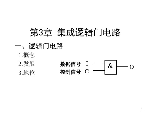
定义时,只用一个输入端,当有2个或2个以上输 入端并联时,输入电流如何?
1 2
IIS
&
IIS
2IIH
IIH &
UIH
30
作业题 3.1 (a) 3.2 3.3
31
(1)电压传输特性
uO/V a b 3.0
c 2.0
1.0
de
V
0 0.5 1.0UT1.5 uI/V
Vcc
&
+
_uI
uO V
(a)电压传输特性
(b)测试电路
图3.2.3 TTL与非门电压传输特性
22
①ab段(截止区): uI<0.6V, T1深饱和 uB2<0.7V, uO=3.4V
结论: UI=0.2V时,T1深饱和 ②bc段(线性区):0.6 V<uI<1.3V,
最大拉电流的确定:
(iD=0)
14
15
(a)灌电流负载等效图
16
图3.1.5负载等效电路
17
第二节 TTL门电路
一、 典型TTL与非门 1.电路结构:
输入级、 中间级、 输出级
18
图3.2.1典型 TTL与非门
(a)电路
A
&
F
B
(b)逻辑符号
19
图3.2.2 T1结构及输入级逻辑等效电路
0.4V
UNL 0 0
uO
uI
uO uI
1
1
0.8V
G1
G2
图3.2.4输入端噪声容限示意图
27
数字电路第三章习题答案
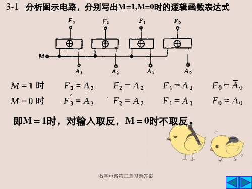
解: 根据题意,该控制电路有三个输入A,B,C; 三个输出G, Y,R。G代表绿灯,Y代表黄灯,R代表红灯。状态赋值如下:1 表示水在电极之上,0表示水在电极之下; 0表示灯亮,1表示灯灭。 按照题意列出的真值表如下。由真值表画出的卡诺图:
数字电路第三章习题答案
3-11
GABAB YABCABC RC
F10 C DAB
F30 CD AB
F20 C DAB
F40 CDAB
解:5号译码器因 E5 0 ,始终处于译码器状态。而1号,2号,3号,4号译码器要受
5号译码器输出控制。(1)当 CD=00时, 只1号译码器译码,其他译码器不译码。当
CD=01时, 只2号译码器译码。(3)当 CD=10时, 只3号译码器译码。当 CD=11时,
Y 1AB A C (B C ) m (1,2,3,7) Y2ABAB m (2,3,4,5)
Y3(AB)(AC) m (0,1,5,7)
Y4ABC ABC m(0,7)
解:先进行化简变换为最小相之和形式:
Y 1 A A B B A C C A A B B C A B C A B C C A BC
数字电路第三章习题答案
3-13 F ( A 3 B 3 ) • ( A 2 B 2 ) A 1 (B 1 ) A 0 ( B 0 )
A和B相等的条件是:最高位相等并且低三位也相等。 所以有:
(A3B3)1 (A 2 B 2 )A 1 ( B 1 )A 0 ( B 0 ) 1 可以把 (A3B3)作为74138待分配的数据,加载到G1控 制端;A2A1A0,B2B1B0分别作为138和151的通道选
数字电路第三章习题答案
3-5 列出题示逻辑图的真值表。图中T331为输出低电平有效的8421码译码器。
数字电路第三章习题与答案

第三章集成逻辑门电路一、选择题1. 三态门输出高阻状态时,()是正确的说法。
A.用电压表测量指针不动B.相当于悬空C.电压不高不低D.测量电阻指针不动2. 以下电路中可以实现“线与”功能的有()。
A.与非门B.三态输出门C.集电极开路门D.漏极开路门3.以下电路中常用于总线应用的有()。
A.TSL门B.OC门C. 漏极开路门D.CMOS与非门4.逻辑表达式Y=AB可以用()实现。
A.正或门B.正非门C.正与门D.负或门5.TTL电路在正逻辑系统中,以下各种输入中()相当于输入逻辑“1”。
A.悬空B.通过电阻2.7kΩ接电源C.通过电阻2.7kΩ接地D.通过电阻510Ω接地6.对于TTL与非门闲置输入端的处理,可以()。
A.接电源B.通过电阻3kΩ接电源C.接地D.与有用输入端并联7.要使TTL与非门工作在转折区,可使输入端对地外接电阻RI()。
A.>RONB.<ROFFC.ROFF<RI<ROND.>ROFF8.三极管作为开关使用时,要提高开关速度,可( )。
A.降低饱和深度B.增加饱和深度C.采用有源泄放回路D.采用抗饱和三极管9.CMOS数字集成电路与TTL数字集成电路相比突出的优点是()。
A.微功耗B.高速度C.高抗干扰能力D.电源范围宽10.与CT4000系列相对应的国际通用标准型号为()。
A.CT74S肖特基系列B. CT74LS低功耗肖特基系列C.CT74L低功耗系列D. CT74H高速系列11.电路如图(a),(b)所示,设开关闭合为1、断开为0;灯亮为1、灯灭为0。
F 对开关A、B、C的逻辑函数表达式()。
F1F 2(a)(b)A.C AB F =1 )(2B A C F += B.C AB F =1 )(2B A C F +=C. C B A F =2 )(2B A C F += 12.某TTL 反相器的主要参数为IIH =20μA ;IIL =1.4mA ;IOH =400μA ;水IOL =14mA ,带同样的门数( )。
数字电路第三章习题与答案
第三章集成逻辑门电路一、选择题1、三态门输出高阻状态时,( )就是正确的说法。
A、用电压表测量指针不动B、相当于悬空C、电压不高不低D、测量电阻指针不动2、以下电路中可以实现“线与”功能的有( )。
A、与非门B、三态输出门C、集电极开路门D、漏极开路门3.以下电路中常用于总线应用的有( )。
A、TSL门B、OC门C、漏极开路门D、CMOS与非门4.逻辑表达式Y=AB可以用( )实现。
A、正或门B、正非门C、正与门D、负或门5.TTL电路在正逻辑系统中,以下各种输入中( )相当于输入逻辑“1”。
A、悬空B、通过电阻2、7kΩ接电源C、通过电阻2、7kΩ接地D、通过电阻510Ω接地6.对于TTL与非门闲置输入端的处理,可以( )。
A、接电源B、通过电阻3kΩ接电源C、接地D、与有用输入端并联7.要使TTL与非门工作在转折区,可使输入端对地外接电阻RI( )。
A、>RONB、<ROFFC、ROFF<RI<ROND、>ROFF8.三极管作为开关使用时,要提高开关速度,可( )。
A、降低饱与深度B、增加饱与深度C、采用有源泄放回路D、采用抗饱与三极管9.CMOS数字集成电路与TTL数字集成电路相比突出的优点就是( )。
A、微功耗B、高速度C、高抗干扰能力D、电源范围宽10.与CT4000系列相对应的国际通用标准型号为( )。
A、CT74S肖特基系列B、 CT74LS低功耗肖特基系列C、CT74L低功耗系列D、 CT74H高速系列11.电路如图(a),(b)所示,设开关闭合为1、断开为0;灯亮为1、灯灭为0。
F 对开关A、B、C的逻辑函数表达式( )。
F1F 2(a)(b)A.C AB F =1 )(2B A C F +=B.C AB F =1 )(2B A C F +=C. C B A F =2 )(2B A C F +=12.某TTL 反相器的主要参数为IIH =20μA;IIL =1、4mA;IOH =400μA;水IOL =14mA,带同样的门数( )。
数字电子技术基础-第3章课后习题答案
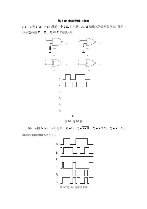
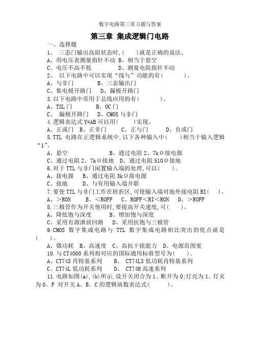
第3章集成逻辑门电路3-1 如图3-1a)~d)所示4个TTL门电路,A、B端输入的波形如图e)所示,试分别画出F1、F2、F3和F4的波形图。
A1A234a)b)c)d)F1F2F3F4BAe)图3-1 题3-1图解:从图3-1a)~d)可知,11F=,2F A B=+,3F A B=⊕,4F A B= ,输出波形图如图3-2所示。
F1F2F3F4AB图3-2题3-1输出波形图3-2 电路如图3-3a )所示,输入A 、B 的电压波形如图3-3b )所示,试画出各个门电路输出端的电压波形。
1A 23b)a)AB图3-3 题3-2图解:从图3-3a )可知,1F AB =,2F A B =+,3F A B =⊕,输出波形如图3-4所示。
F 1F 2F 3AB图3-4 题3-2输出波形3-3在图3-5a )所示的正逻辑与门和图b )所示的正逻辑或门电路中,若改用负逻辑,试列出它们的逻辑真值表,并说明F 和A 、B 之间是什么逻辑关系。
b)a)图3-5 题3-3图解:(1)图3-5a )负逻辑真值表如表3-1所示。
表3-1 与门负逻辑真值表F 与A 、B 之间相当于正逻辑的“或”操作。
(2)图3-5b )负逻辑真值表如表3-2所示。
表3-2 或门负逻辑真值表F 与A 、B 之间相当于正逻辑的“与”操作。
3-4试说明能否将与非门、或非门和异或门当做反相器使用?如果可以,各输入端应如何连接?解:与非门、或非门和异或门经过处理以后均可以实现反相器功能。
1)与非门:将多余输入端接至高电平或与另一端并联; 2)或非门:将多余输入端接至低电平或与另一端并联;3) 异或门:将另一个输入端接高电平。
3-5为了实现图3-6所示的各TTL 门电路输出端所示的逻辑关系,请合理地将多余的输入端进行处理。
b)a)AB=A B=+A BC DABC D图3-6 题3-5图解:a )多余输入端可以悬空,但建议接高电平或与另两个输入端的一端相连;b )多余输入端接低电平或与另两个输入端的一端相连;c) 未用与门的两个输入端至少一端接低电平,另一端可以悬空、接高电平或接低电平;d )未用或门的两个输入端悬空或都接高电平。
- 1、下载文档前请自行甄别文档内容的完整性,平台不提供额外的编辑、内容补充、找答案等附加服务。
- 2、"仅部分预览"的文档,不可在线预览部分如存在完整性等问题,可反馈申请退款(可完整预览的文档不适用该条件!)。
- 3、如文档侵犯您的权益,请联系客服反馈,我们会尽快为您处理(人工客服工作时间:9:00-18:30)。
0. Explain qualitatively
4
Chapter 3 Problem Set a. Write down the equations (and only those) which are needed to determine the voltage at node X. Do NOT plug in any values yet. Neglect short channel effects and assume that λp = 0. b. Draw the (approximative) load lines for both MOS transistor and resistor. Mark some of the significant points. c. Determine the required width of the transistor (for L = 0.25µm) such that X equals 1.5 V. d. We have, so far, assumed that M1 is a long-channel device. Redraw the load lines assuming that M1 is velocity-saturated. Will the voltage at X rise or fall?
Table 0.2 Measurements taken from the MOS device, at different terminal voltages.
Measurement number 1 2 3 4 5 6 7 8.
VGS (V) -2.5 1 -0.7 -2.0 -2.5 -2.5 -2.5
R1 = 2kΩ + 2.5 V – ID R2 = 2kΩ
+ VD –
Figure 0.1
Resistor diode circuit.
2.
[M, None, 3.2.3] For the circuit in Figure 0.2, Vs = 3.3 V. Assume AD = 12 µm2, φ0 = 0.65 V, and m = 0.5. NA = 2.5 E16 and ND = 5 E15. a. Find ID and VD. b. Is the diode forward- or reverse-biased? c. Find the depletion region width, Wj, of the diode. d. Use the parallel-plate model to find the junction capacitance, Cj. e. Set Vs = 1.5 V. Again using the parallel-plate model, explain qualitatively why Cj increases.
VDD = 2.5V R VD Vin=2V M1
W/L = 2.5µ/0.25µ
VS
I = 50µΑ
Figure 0.4 Test configuration for the NMOS device.
9.
a. When R =10kΩ find the operation region, VD and VS. b. When R= 30kΩ again determine the operation region VD, VS c. For the case of R = 10kΩ, would VS increase or decrease if λ ≠ [M, None, 3.3.2] Consider the circuit configuration of Figure 0.5.
Digital Integrated Circuits - 2nd Ed
3
e. Given the obtained answers, determine for each of the measurements the operation region of the transistor (choose from cutoff, resistive, saturated, and velocity saturated). Annotate your finding in the right-most column of the above.
Measured NMOS transistor data VGS VDS 1.8 1.8 2.5 1.8 1.8 VBS 0 0 0 –1 -2 ID (µA) 1812 1297 1361 1146 1039
Table 0.1
1 2 3 4 5 7.
2.5 2 2 2 2
[E, None, 3.3.2] Given Table 0.2 ,the goal is to derive the important device parameters from these data points. As the measured transistor is processed in a deep-submciron technology, the ‘unified model’ holds. From the material constants, we also could determine that the saturation voltage VDSAT equals -1V. You may also assume that -2ΦF = -0.6V. NOTE: The parameter values on Table 3.3 do NOT hold for this problem. a. Is the measured transistor a PMOS or an NMOS device? Explain your answer. b. Determine the value of VT0. c. Determine γ. d -0.8 -2.5 -2.5 -1.5 -0.8
VSB (V) 0 0 0 0 -1 0 0
ID (µA) -84.375 0.0 -1.04 -56.25 -72.0 -80.625 -66.56
Operation Region?
[M, None, 3.3.2] An NMOS device is plugged into the test configuration shown below in Figure 0.4. The input Vin =2V. The current source draws a constant current of 50 µA. R is a variable resistor that can assume values between 10kΩ and 30 kΩ. Transistor M1 experiences short channel effects and has following transistor parameters: k’ = 110*10-6 V/A2, VT = 0.4 , and VDSAT = 0.6V. The transistor has a W/L = 2.5µ/0.25µ. For simplicity body effect and channel length modulation can be neglected. i.e λ=0, γ=0. .
2
Chapter 3 Problem Set
G
D ID S G
S ID D Figure 0.3 NMOS and PMOS devices.
5.
6.
a. NMOS W = 1.2µm, L = 0.25µm b. NMOS W = 4.8µm, L = 0.5µm c. PMOS W = 1.2 µm, L = 0.25 µm d. PMOS W = 4.8 µm, L = 0.5 µm [E, SPICE, 3.3.2] Indicate on the plots from problem 4. a. the regions of operation. b. the effects of channel length modulation. c. Which of the devices are in velocity saturation? Explain how this can be observed on the IV plots. [M, None, 3.3.2] Given the data in Table 0.1 for a short channel NMOS transistor with VDSAT = 0.6 V and k′ =100 µA/V2, calculate VT0, γ, λ, 2|φf|, and W / L:
Rs = 2 kΩ + Vs=3.3V – – VD +
ID
Figure 0.2
Series diode circuit
3.
4.
[E, None, 3.3.2] Figure 0.3 shows NMOS and PMOS devices with drains, source, and gate ports annotated. Determine the mode of operation (saturation, linear, or cutoff) and drain current ID for each of the biasing configurations given below. Verify with SPICE. Use the follow2 –1 ing transistor data: NMOS: k' n = 115µA/V , VT0 = 0.43 V, λ = 0.06 V , PMOS: k' p = 30 2 –1 µA/V , VT0 = –0.4 V, λ = -0.1 V . Assume (W/L) = 1. a. NMOS: VGS = 2.5 V, VDS = 2.5 V. PMOS: VGS = –0.5 V, VDS = –1.25 V. b. NMOS: VGS = 3.3 V, VDS = 2.2 V. PMOS: VGS = –2.5 V, VDS = –1.8 V. c. NMOS: VGS = 0.6 V, VDS = 0.1 V. PMOS: VGS = –2.5 V, VDS = –0.7 V. [E, SPICE, 3.3.2] Using SPICE plot the I-V characteristics for the following devices.