LM3886制作的低音炮电路图
LM386低电压音频功率放大器的原理与典型应用电路(完整资料).doc

【最新整理,下载后即可编辑】LM386低电压音频功率放大器的原理与典型应用电路图一、特性原理The LM386 is a power amplifier designed for use in low voltage consumer applications. The gain is internally set to 20 to keep external part count low, but the addition of an external resistor and capacitor between pins 1 and 8 will increase the gain to any value from 20 to 200。
The inputs are ground referenced while the output automatically biases to one-half the supply voltage. The quiescent power drain is only 24 milliwatts when operating from a 6 volt supply, making the LM386 ideal for battery operation。
LM386是美国国家半导体公司生产的音频功率放大器,主要应用于低电压消费类产品。
为使外围元件最少,电压增益内置为20。
但在1脚和8脚之间增加一只外接电阻和电容,便可将电压增益调为任意值,直至200。
输入端以地位参考,同时输出端被自动偏置到电源电压的一半,在6V电源电压下,它的静态功耗仅为24mW,使得LM386特别适用于电池供电的场合。
LM386的封装形式有塑封8引线双列直插式和贴片式。
贴片封装形式SOPLM386特性(Features):* 静态功耗低,约为4mA,可用于电池供电。
* 工作电压范围宽,4-12V or 5-18V。
车载有源低音炮电路图
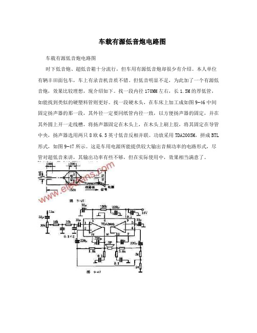
车载有源低音炮电路图车载有源低音炮电路图时下低音炮、超低音箱十分流行,但车用有源低音炮却很少有介绍。
本人单位有辆丰田面包车,车上有录音机音质不错。
但低音明显不足,为此加了一个有源低音炮,效果比较理想,现介绍如下。
找一段内径170MM左右,长1.5M的厚低管,如能找到类似的硬塑料管则更好。
找一段硬木头,在车床上加工成如图9-46中间固定扬声器的那一段,其外径一定要同纸管内径一致,以方便扬声器的固定,并在其外圆上开一走线槽,将扬声器固定在木头上,在木头上刷上胶,将其固定在导管中央,扬声器选用两只8欧6.5英寸低音反相并联。
功放采用TDA2005M,拼成BTL 形式,如图9-47所示。
这是车用电源所能提供较大输出音频功率的电路形式,尽管对超低音来讲,其输出功率有些不够,但在实际使用中,效果相当满意了。
使用时将低音炮旋转在车后座下,低音信号可直接从扬声器上拾取,注意相位不要接错。
此低音炮如能配置50W以上超低音功放、用于家庭影院系统,其效果也较好。
school)], 4 4 house building as well as more than 1000 copies of books, more than 10 kinds of collection of newspapers and magazines, fires burnt down. In 1938, the Japanese learned that the national Government established in XI Tang Tomb rotten "clip" taxes, tax officers live in 8 of Yan Dong village farmers home, troops at night, Yao was burned several houses. 1938 new morning of September 18, the Japanese team went to the countryside "sweep" from the kaiyang village line to Tung Yang Jia Qiao yan Temple wall and met Yang Jia溇 Zhou Dana (male) weeks because of long-term illness and can't work in the fields, the Japanese see his face from scratch without calluses, regard him as "Shina", thrust a knife at the scene of his death. The body was stabbed 7 times, wound 13. The same day, Trang bang village heard the Japanese come to "mop-up" are hiding, mother of 9 Zhou Guanbao Zhang Aying todrill a "dry mound", was discovered by the Japanese, a shot in the end. The same day, is 7 zhouhaijiangzhi grandfather Zhou Yingbao to escape the Japanese army, was found on the road, a shot in the end. In March 1939, the Japanese army in Yan Tomb raiding, has arrested 16 people, in fengqiao cigarettes this morning bang, killing 11 people on the River, East meeting point in wood qiaotu in the afternoon killing 4 people on the Riverside. Gu Tong is a Japanese go speak the Shanghai dialect,later to be called Gu Tong as "kill left." On January 18, 1943, theelves, five thousand or six thousand, water and land go hand in hand "mop-up" jiaxing area west of the railway, Yan Tomb area fall. March 6, Niu Shan (County Government II section chief) carrying its child Niu Jun (strict Tomb seventh district Chang) and the District Assistant Yu Xuchu, and players Jin Fuqin, and Shen Baosheng, six people received Wujiang underground County Government notification低成本超重低音炮电路及制作市售的国产有源超重低音音箱价格一般均在1200元以上,进口的产品售价更是价格不菲、本文向读者介绍一款自制的有源超重低音音箱,输出功率达100W,最低频率响应可达26HZ,制作成本500元左右。
制作LM3886动态负反馈功放,喇叭保护部分贴片PCB文件

制作LM3886动态负反馈功放,喇叭保护部分贴片PCB文件软件类型:国产软件授权方式:共享软件界面语言:简体中文软件大小:未知文件类型:.rar 运行环境:Win2003,WinXP,Win2000,Win9X 软件等级:★★★☆☆ 发布时间:2013-03-09 官方网址:http:// 演示网址:http:// 下载次数: 216 软件介绍刚好今天公司没有事情下午搞了张图,大家帮忙看下有啥修改的地方,建议的等板子出来后都有送线路图以上,我想把PCB在加个保护电路上去,我是打算玩多媒体的,所以前级我不打算加了。
下载地址•3886•lm3886•laba下载说明因为下载很占服务器资源,网站运营成本很高,所以软件全部限制为会员下载,请大家理解和支持☉推荐使用第三方专业下载工具下载本站软件,使用WinRARv3.10 以上版本解压本站软件。
☉如果这个软件总是不能下载的请点击报告错误,谢谢合作!!☉下载本站资源,如果服务器暂不能下载请过一段时间重试!☉如果遇到什么问题,请到本站论坛去咨寻,我们将在那里提供更多、更好的资源!☉本站提供的一些商业软件是供学习研究之用,如用于商业用途,请购买正版。
不错(1)100.00%一般(0)0.00%相关文章•制作lm3886功放全套PCB文件•diy制作LM3886功放的Sch+PCB文件下载你可能感兴趣的文章•大字符1602制作时钟电子钟原理图和PC•仿制矿石许剑伟老师的数字电桥程序•TA2024数字功放pcb文件•电路设计PCB设计经验谈文档PDF下载•马碲斯胆前级PCB(感光油) PDF文件下------分隔线----------------------------•上一篇:制作lm3886功放全套PCB文件•下一篇:diy制作AD1955 解码器 DAC PCB文件•收藏•挑错•推荐•打印。
LM3886
LM3886Overture ™Audio Power Amplifier SeriesHigh-Performance68W Audio Power Amplifier w/MuteGeneral DescriptionThe LM3886is a high-performance audio power amplifier capable of delivering 68W of continuous average power to a 4Ωload and 38W into 8Ωwith 0.1%(THD +N)from 20Hz–20kHz.The performance of the LM3886,utilizing its Self Peak In-stantaneous Temperature (˚Ke)(SPiKe ™)Protection Cir-cuitry,puts it in a class above discrete and hybrid amplifiers by providing an inherently,dynamically protected Safe Oper-ating Area (SOA).SPiKe Protection means that these parts are completely safeguarded at the output against overvolt-age,undervoltage,overloads,including shorts to the sup-plies,thermal runaway,and instantaneous temperature peaks.The LM3886maintains an excellent Signal-to-Noise Ratio of greater than 92dB with a typical low noise floor of 2.0µV.It exhibits extremely low (THD +N)values of 0.03%at the rated output into the rated load over the audio spectrum,and provides excellent linearity with an IMD (SMPTE)typical rat-ing of 0.004%.Featuresn 68W cont.avg.output power into 4Ωat V CC =±28Vn 38W cont.avg.output power into 8Ωat V CC =±28V n 50W cont.avg.output power into 8Ωat V CC =±35V n 135W instantaneous peak output power capability n Signal-to-Noise Ratio ≥92dB n An input mute functionnOutput protection from a short to ground or to the supplies via internal current limiting circuitryn Output over-voltage protection against transients from inductive loadsn Supply under-voltage protection,not allowing internal biasing to occur when |V EE |+|V CC |≤12V,thus eliminating turn-on and turn-off transients n 11-lead TO-220package Applicationsn Component stereo n Compact stereon Self-powered speakers n Surround-sound amplifiers nHigh-end stereo TVsTypical ApplicationOverture ™and SPiKe ™Protection are trademarks of National Semiconductor Corporation.DS011833-1*Optional components dependent upon specific design requirements.Refer to the External Components Description section for a component functional description.FIGURE 1.Typical Audio Amplifier Application CircuitMay 1999LM3886Overture Audio Power Amplifier Series High-Performance 68W Audio Power Amplifier w/Mute©1999National Semiconductor Corporation Connection DiagramPlastic Package(Note12)DS011833-2 Note1:Preliminary:call you local National Sales Rep.or distributor for availabilityTop ViewOrder Number LM3886Tor LM3886TFSee NS Package Number TA11B forStaggered Lead Non-IsolatedPackage or TF11B(Note1)forStaggered Lead Isolated Package 2Absolute Maximum Ratings(Notes6,5)If Military/Aerospace specified devices are required, please contact the National Semiconductor Sales Office/ Distributors for availability and specifications.Supply Voltage|V+|+|V−|(No Signal)94V Supply Voltage|V+|+|V−|(Input Signal)84V Common Mode Input Voltage(V+or V−)and|V+|+|V−|≤80V Differential Input Voltage(Note16)60V Output Current Internally Limited Power Dissipation(Note7)125W ESD Susceptibility(Note8)3000V Junction Temperature(Note9)150˚C Soldering InformationT Package(10seconds)260˚C Storage Temperature−40˚C to+150˚C Thermal ResistanceθJC1˚C/W θJA43˚C/W Operating Ratings(Notes5,6)Temperature RangeT MIN≤T A≤T MAX−20˚C≤T A≤+85˚C Supply Voltage|V+|+|V−|20V to84VElectrical Characteristics(Notes5,6)The following specifications apply for V+=+28V,V−=−28V,I MUTE=−0.5mA with R L=4Ωunless otherwise specified.Limits apply for T A=25˚C.Symbol Parameter ConditionsLM3886Units(Limits) Typical(Note10)Limit(Note11)|V+|+|V−|Power Supply Voltage(Note14)V pin7−V−≥9V182084V(min)V(max)A M Mute Attenuation Pin8Open or at0V,Mute:OnCurrent out of Pin8>0.5mA,Mute:Off11580dB(min)P O (Note4)Output Power(Continuous Average)THD+N=0.1%(max)f=1kHz;f=20kHz|V+|=|V−|=28V,R L=4Ω|V+|=|V−|=28V,R L=8Ω|V+|=|V−|=35V,R L=8Ω6838506030W(min)W(min)WPeak P O Instantaneous Peak Output Power135W THD+N Total Harmonic Distortion Plus Noise60W,R L=4Ω,30W,R L=8Ω,20Hz≤f≤20kHz A V=26dB 0.030.03%%SR (Note4)Slew Rate(Note13)V IN=2.0Vp-p,t RISE=2ns198V/µs(min)I+(Note4)Total Quiescent Power SupplyCurrent V CM=0V,V o=0V,I o=0A5085mA(max)V OS (Note3)Input Offset Voltage V CM=0V,I o=0mA110mV(max)I B Input Bias Current V CM=0V,I o=0mA0.21µA(max) I OS Input Offset Current V CM=0V,I o=0mA0.010.2µA(max) I o Output Current Limit|V+|=|V−|=20V,t ON=10ms,V O=0V11.57A(min)V od (Note3)Output Dropout Voltage(Note15)|V+–V O|,V+=28V,I o=+100mA|V O–V−|,V−=−28V,I o=−100mA1.62.52.03.0V(max)V(max)PSRR (Note3)Power Supply Rejection Ratio V+=40V to20V,V−=−40V,V CM=0V,I o=0mAV+=40V,V−=−40V to−20V,V CM=0V,I o=0mA1201058585dB(min)dB(min)CMRR (Note3)Common Mode Rejection Ratio V+=60V to20V,V−=−20V to−60V,V CM=20V to−20V,I o=0mA11085dB(min)A VOL (Note3)Open Loop Voltage Gain|V+|=|V−|=28V,R L=2kΩ,∆V O=40V11590dB(min)GBWP Gain-Bandwidth Product|V+|=|V−|=30Vf O=100kHz,V IN=50mVrms 82MHz(min)3Electrical Characteristics(Notes5,6)(Continued)The following specifications apply for V+=+28V,V−=−28V,I MUTE=−0.5mA with R L=4Ωunless otherwise specified.Limits apply for T A=25˚C.Symbol Parameter ConditionsLM3886Units(Limits) Typical(Note10)Limit(Note11)e IN (Note4)Input Noise IHF—A Weighting FilterR IN=600Ω(Input Referred)2.010µV(max)SNR Signal-to-Noise Ratio P O=1W,A-Weighted,Measured at1kHz,R S=25Ω92.5dBP O=60W,A-Weighted,Measured at1kHz,R S=25Ω110dBIMD Intermodulation Distortion Test60Hz,7kHz,4:1(SMPTE)60Hz,7kHz,1:1(SMPTE)0.0040.009%Note2:Operation is guaranteed up to84V,however,distortion may be introduced from SPIKe Protection Circuitry if proper thermal considerations are not taken into account.Refer to the Thermal Considerations section for more information.(See SPIKe Protection Response)Note3:DC Electrical Test;refer to Test Circuit#1.Note4:AC Electrical Test;refer to Test Circuit#2.Note5:All voltages are measured with respect to the GND pin(pin7),unless otherwise specified.Note6:Absolute Maximum Ratings indicate limits beyond which damage to the device may occur.Operating Ratings indicate conditions for which the device is functional,but do not guarantee specific performance limits.Electrical Characteristics state DC and AC electrical specifications under particular test conditions which guarantee specific performance limits.This assumes that the device is within the Operating Ratings.Specifications are not guaranteed for parameters where no limit is given,however,the typical value is a good indication of device performance.Note7:For operating at case temperatures above25˚C,the device must be derated based on a150˚C maximum junction temperature and a thermal resistance of θJC=1.0˚C/W(junction to case).Refer to the Thermal Resistance figure in the Application Information section under Thermal Considerations.Note8:Human body model,100pF discharged through a1.5kΩresistor.Note9:The operating junction temperature maximum is150˚C,however,the instantaneous Safe Operating Area temperature is250˚C.Note10:Typicals are measured at25˚C and represent the parametric norm.Note11:Limits are guaranteed to National’s AOQL(Average Outgoing Quality Level).Note12:The LM3886T package TA11B is a non-isolated package,setting the tab of the device and the heat sink at V−potential when the LM3886is directly mounted to the heat sink using only thermal compound.If a mica washer is used in addition to thermal compound,θCS(case to sink)is increased,but the heat sink will be isolated from V−.Note13:The feedback compensation network limits the bandwidth of the closed-loop response and so the slew rate will be reduced due to the high frequency roll-off.Without feedback compensation,the slew rate is typically larger.Note14:V−must have at least−9V at its pin with reference to ground in order for the under-voltage protection circuitry to be disabled.Note15:The output dropout voltage is the supply voltage minus the clipping voltage.Refer to the Clipping Voltage vs Supply Voltage graph in the Typical Perfor-mance Characteristics section.Note16:The Differential Input Voltage Absolute Maximum Rating is based on supply voltages of V+=+40V and V−=−40V.Test Circuit#1(DC Electrical Test Circuit)DS011833-34Test Circuit#2(AC Electrical Test Circuit)DS011833-4Single Supply Application CircuitDS011833-5*Optional components dependent upon specific design requirements.Refer to the ExternalComponents Description section for a component functional description.FIGURE2.Typical Single Supply Audio Amplifier Application Circuit5Equivalent Schematic(excluding active protection circuitry)6External Components Description(Figure1and Figure2)Components Functional Description1.R IN Acts as a volume control by setting the voltage level allowed to the amplifier’s input terminals.2.R A Provides DC voltage biasing for the single supply operation and bias current for the positive input terminal.3.C A Provides bias filtering.4.C Provides AC coupling at the input and output of the amplifier for single supply operation.5.R B Prevents currents from entering the amplifier’s non-inverting input which may be passed through to the loadupon power-down of the system due to the low input impedance of the circuitry when the under-voltagecircuitry is off.This phenomenon occurs when the supply voltages are below1.5V.6.C C(Note17)Reduces the gain(bandwidth of the amplifier)at high frequencies to avoid quasi-saturation oscillations of the output transistor.The capacitor also suppresses external electromagnetic switching noise created from fluorescent lamps.7.Ri Inverting input resistance to provide AC Gain in conjunction with R f1.8.Ci(Note17)Feedback capacitor.Ensures unity gain at DC.Also a low frequency pole(highpass roll-off)at: f c=1/(2πRi Ci)9.R f1Feedback resistance to provide AC Gain in conjunction with Ri.10.R f2(Note17)At higher frequencies feedback resistance works with C f to provide lower AC Gain in conjunction with R f1 and Ri.A high frequency pole(lowpass roll-off)exists at:f c=[R f1R f2(s+1/R f2C f)]/[(R f1+R f2)(s+1/C f(R f1+R f2))]11.C f(Note17)Compensation capacitor that works with R f1and R f2to reduce the AC Gain at higher frequencies.12.R M Mute resistance set up to allow0.5mA to be drawn from pin8to turn the muting function off.→RMis calculated using:R M≤(|V EE|−2.6V)/I8where I8≥0.5mA.Refer to the Mute Attenuation vs.Mute Current curves in the Typical Performance Characteristics section.13.C M Mute capacitance set up to create a large time constant for turn-on and turn-off muting.14.R SN(Note17)Works with C SN to stabilize the output stage by creating a pole that eliminates high frequency oscillations.15.C SN(Note17)Works with R SN to stabilize the output stage by creating a pole that eliminates high frequency oscillations.f c=1/(2πR SN C SN)16.L(Note17)Provides high impedance at high frequencies so that R may decouple a highly capacitive load and reduce the Q of the series resonant circuit due to capacitive load.Also provides a low impedance at low frequencies to short out R and pass audio signals to the load.17.R(Note17)18.C S Provides power supply filtering and bypassing.19.S1Mute switch that mutes the music going into the amplifier when opened.Note17:Optional components dependent upon specific design requirements.Refer to the Application Information section for more information.OPTIONAL EXTERNAL COMPONENT INTERACTIONAlthough the optional external components have specific desired functions that are designed to reduce the bandwidth and elimi-nate unwanted high frequency oscillations they may cause certain undesirable effects when they interact.Interaction may occurfor components whose reactances are in close proximity to one another.One example would be the coupling capacitor,C C,andthe compensation capacitor,C f.These two components act as low impedances to certain frequencies which will couple signals from the input to the output.Please take careful note of basic amplifier component functionality when designing in these compo-nents.The optional external components shown in Figure2and described above are applicable in both single and split voltage supply configurations.7Typical Performance CharacteristicsSafeAreaDS011833-18SPiKeProtection ResponseDS011833-19Supply Current vs Supply VoltageDS011833-20Pulse Thermal Resistance DS011833-21Pulse Thermal ResistanceDS011833-65Supply Current vs Output VoltageDS011833-22Pulse Power Limit DS011833-23Pulse Power LimitDS011833-24Supply Current vs Case TemperatureDS011833-25 8Typical Performance Characteristics(Continued)Input Bias Current vs Case TemperatureDS011833-26Clipping Voltage vs Supply VoltageDS011833-27Clipping Voltage vs Supply VoltageDS011833-28THD +N vs Frequency DS011833-29THD +N vs Frequency DS011833-30THD +N vs FrequencyDS011833-31THD +N vs Output Power DS011833-32THD +N vs Output Power DS011833-33THD +N vs Output PowerDS011833-34THD +N vs Output Power DS011833-35THD +N vs Output Power DS011833-36THD +N vs Output PowerDS011833-379Typical Performance Characteristics(Continued)THD +N vs Output PowerDS011833-38THD +N vs Output PowerDS011833-39THD +N vs Output PowerDS011833-40THD +N Distribution DS011833-41THD +N Distribution DS011833-42THD +N DistributionDS011833-43THD +N Distribution DS011833-44THD +N DistributionDS011833-45Output Power vs Load ResistanceDS011833-46 10Typical Performance Characteristics(Continued)Max Heatsink Thermal Resistance(˚C/W)at the Specified Ambient Temperature(˚C)Maximum Power Dissipation vs Supply VoltageDS011833-9 Note:The maximum heat sink thermal resistance values,øSA,in the table above were calculated using aøCS=0.2˚C/W due to thermal compound.Power Dissipationvs Output PowerDS011833-47Power Dissipationvs Output PowerDS011833-48Output Powervs Supply VoltageDS011833-49IMD60Hz,4:1DS011833-50IMD60Hz,7kHz,4:1DS011833-51IMD60Hz,7kHz,4:1DS011833-52 11Typical Performance Characteristics(Continued)Application InformationGENERAL FEATURESMute Function:The muting function of the LM3886allows the user to mute the music going into the amplifier by draw-ing less than 0.5mA out of pin 8of the device.This is accom-plished as shown in the Typical Application Circuit where the resistor R M is chosen with reference to your negative supply voltage and is used in conjuction with a switch.The switch (when opened)cuts off the current flow from pin 8to V −,thus placing the LM3886into mute mode.Refer to the Mute At-tenuation vs Mute Current curves in the Typical Perfor-mance Characteristics section for values of attenuation per current out of pin 8.The resistance R M is calculated by the following equation:R M (|V EE |−2.6V)/I8where I8≥0.5mA.Under-Voltage Protection:Upon system power-up the under-voltage protection circuitry allows the power supplies and their corresponding caps to come up close to their full values before turning on the LM3886such that no DC output spikes occur.Upon turn-off,the output of the LM3886is brought to ground before the power supplies such that no transients occur at power-down.IMD 60Hz,1:1DS011833-53IMD 60Hz,7kHz 1:1DS011833-54IMD 60Hz,7kHz,1:1DS011833-55Mute Attenuation vs Mute CurrentDS011833-56Mute Attenuation vs Mute CurrentDS011833-57Large Signal ResponseDS011833-58Power Supply Rejection RatioDS011833-59Common-Mode Rejection RatioDS011833-60Open LoopFrequency ResponseDS011833-6112Application Information(Continued)Over-Voltage Protection:The LM3886contains overvolt-age protection circuitry that limits the output current to ap-proximately 11Apeak while also providing voltage clamping,though not through internal clamping diodes.The clamping effect is quite the same,however,the output transistors are designed to work alternately by sinking large current spikes.SPiKe Protection:The LM3886is protected from instanta-neous peak-temperature stressing by the power transistor array.The Safe Operating Area graph in the Typical Perfor-mance Characteristics section shows the area of device operation where the SPiKe Protection Circuitry is not en-abled.The waveform to the right of the SOA graph exempli-fies how the dynamic protection will cause waveform distor-tion when enabled.Thermal Protection:The LM3886has a sophisticated ther-mal protection scheme to prevent long-term thermal stress to the device.When the temperature on the die reaches 165˚C,the LM3886shuts down.It starts operating again when the die temperature drops to about 155˚C,but if the temperature again begins to rise,shutdown will occur again at 165˚C.Therefore the device is allowed to heat up to a relatively high temperature if the fault condition is temporary,but a sustained fault will cause the device to cycle in a Schmitt Trigger fashion between the thermal shutdown tem-perature limits of 165˚C and 155˚C.This greatly reduces the stress imposed on the IC by thermal cycling,which in turn improves its reliability under sustained fault conditions.Since the die temperature is directly dependent upon the heat sink,the heat sink should be chosen as discussed in the Thermal Considerations section,such that thermal shutdown will not be reached during normal ing the best heat sink possible within the cost and space con-straints of the system will improve the long-term reliability of any power semiconductor device.THERMAL CONSIDERATIONSHeat SinkingThe choice of a heat sink for a high-power audio amplifier is made entirely to keep the die temperature at a level such that the thermal protection circuitry does not operate under normal circumstances.The heat sink should be chosen to dissipate the maximum IC power for a given supply voltage and rated load.With high-power pulses of longer duration than 100ms,the case temperature will heat up drastically without the use of a heat sink.Therefore the case temperature,as measured at the center of the package bottom,is entirely dependent on heat sink design and the mounting of the IC to the heat sink.For the design of a heat sink for your audio amplifier applica-tion refer to the Determining The Correct Heat Sink sec-tion.Since a semiconductor manufacturer has no control over which heat sink is used in a particular amplifier design,we can only inform the system designer of the parameters and the method needed in the determination of a heat sink.With this in mind,the system designer must choose his supply voltages,a rated load,a desired output power level,and know the ambient temperature surrounding the device.These parameters are in addition to knowing the maximum junction temperature and the thermal resistance of the IC,both of which are provided by National Semiconductor.As a benefit to the system designer we have provided Maxi-mum Power Dissipation vs Supply Voltages curves for vari-ous loads in the Typical Performance Characteristics sec-tion,giving an accurate figure for the maximum thermal resistance required for a particular amplifier design.This data was based on θJC =1˚C/W and θCS =0.2˚C/W.We also provide a section regarding heat sink determination for any audio amplifier design where θCS may be a different value.It should be noted that the idea behind dissipating the maxi-mum power within the IC is to provide the device with a low resistance to convection heat transfer such as a heat sink.Therefore,it is necessary for the system designer to be con-servative in his heat sink calculations.As a rule,the lower the thermal resistance of the heat sink the higher the amount of power that may be dissipated.This is of course guided by the cost and size requirements of the system.Convection cooling heat sinks are available commercially,and their manufacturers should be consulted for ratings.Proper mounting of the IC is required to minimize the thermal drop between the package and the heat sink.The heat sink must also have enough metal under the package to conduct heat from the center of the package bottom to the fins with-out excessive temperature drop.A thermal grease such as Wakefield type 120or Thermalloy Thermacote should be used when mounting the package to the heat sink.Without this compound,thermal resistance will be no better than 0.5˚C/W,and probably much worse.With the compound,thermal resistance will be 0.2˚C/W or less,assuming under 0.005inch combined flatness runout for the package and heat sink.Proper torquing of the mounting bolts is important and can be determined from heat sink manufacturer’s specification sheets.Should it be necessary to isolate V −from the heat sink,an in-sulating washer is required.Hard washers like beryluum ox-ide,anodized aluminum and mica require the use of thermal compound on both faces.Two-mil mica washers are most common,giving about 0.4˚C/W interface resistance with the compound.Silicone-rubber washers are also available.A 0.5˚C/W ther-mal resistance is claimed without thermal compound.Expe-rience has shown that these rubber washers deteriorate and must be replaced should the IC be dismounted.Determining Maximum Power DissipationPower dissipation within the integrated circuit package is a very important parameter requiring a thorough understand-ing if optimum power output is to be obtained.An incorrect maximum power dissipation (P D )calculation may result in in-adequate heat sinking,causing thermal shutdown circuitry to operate and limit the output power.The following equations can be used to acccurately calculate the maximum and average integrated circuit power dissipa-tion for your amplifier design,given the supply voltage,rated load,and output power.These equations can be directly ap-plied to the Power Dissipation vs Output Power curves in the Typical Performance Characteristics section.Equation (1)exemplifies the maximum power dissipation of the IC and Equations (2),(3)exemplify the average IC power dissipation expressed in different forms.P DMAX =V CC 2/2π2R L (1)where V CC is the total supply voltageP DAVE =(V Opk /R L )[V CC /π−V Opk /2](2)where V CC is the total supply voltage and V Opk =V CC /π13Application Information(Continued)P DAVE=V CC V Opk/πR L−V Opk2/2R L(3)where V CC is the total supply voltage.Determining the Correct Heat SinkOnce the maximum IC power dissipation is known for agiven supply voltage,rated load,and the desired rated out-put power the maximum thermal resistance(in˚C/W)of aheat sink can be calculated.This calculation is made usingEquation(4)and is based on the fact that thermal heat flowparameters are analogous to electrical current flow proper-ties.It is also known that typically the thermal resistance,θJC(junction to case),of the LM3886is1˚C/W and that usingThermalloy Thermacote thermal compound provides a ther-mal resistance,θCS(case to heat sink),of about0.2˚C/W asexplained in the Heat Sinking section.Referring to the figure below,it is seen that the thermal resis-tance from the die(junction)to the outside air(ambient)is acombination of three thermal resistances,two of which areknown,θJC andθCS.Since convection heat flow(power dis-sipation)is analogous to current flow,thermal resistance isanalogous to electrical resistance,and temperature dropsare analogous to voltage drops,the power dissipation out ofthe LM3886is equal to the following:P DMAX=(T Jmax−T Amb)/θJAwhereθJA=θJC+θCS+θSABut since we know P DMAX,θJC,andθSC for the applicationand we are looking forθSA,we have the following:θSA=[(T Jmax−T Amb)−P DMAX(θJC+θCS)]/P DMAX(4)Again it must be noted that the value ofθSA is dependentupon the system designer’s amplifier application and its cor-responding parameters as described previously.If the ambi-ent temperature that the audio amplifier is to be working un-der is higher than the normal25˚C,then the thermalresistance for the heat sink,given all other things are equal,will need to be smaller.Equations(1),(4)are the only equations needed in the de-termination of the maximum heat sink thermal resistance.This is of course given that the system designer knows therequired supply voltages to drive his rated load at a particularpower output level and the parameters provided by the semi-conductor manufacturer.These parameters are the junctionto case thermal resistance,θJC,T Jmax=150˚C,and the rec-ommended Thermalloy Thermacote thermal compound re-sistance,θCS.SIGNAL-TO-NOISE RATIOIn the measurement of the signal-to-noise ratio,misinterpre-tations of the numbers actually measured are common.Oneamplifier may sound much quieter than another,but due toimproper testing techniques,they appear equal in measure-ments.This is often the case when comparing integrated cir-cuit designs to discrete amplifier designs.Discrete transistoramps often“run out of gain”at high frequencies and there-fore have small bandwidths to noise as indicated below.Integrated circuits have additional open loop gain allowingadditional feedback loop gain in order to lower harmonic dis-tortion and improve frequency response.It is this additionalbandwidth that can lead to erroneous signal-to-noise mea-surements if not considered during the measurement pro-cess.In the typical example above,the difference in band-width appears small on a log scale but the factor of10inbandwidth,(200kHz to2MHz)can result in a10dB theoreti-cal difference in the signal-to-noise ratio(white noise is pro-portional to the square root of the bandwidth in a system).In comparing audio amplifiers it is necessary to measure themagnitude of noise in the audible bandwidth by using a“weighting”filter(Note18).A“weighting”filter alters the fre-quency response in order to compensate for the average hu-man ear’s sensitivity to the frequency spectra.The weightingfilters at the same time provide the bandwidth limiting as dis-cussed in the previous paragraph.Note18:CCIR/ARM:A Practical Noise Measurement Method;by RayDolby,David Robinson and Kenneth Gundry,AES Preprint No.1353(F-3).In addition to noise filtering,differing meter types give differ-ent noise readings.Meter responses include:1.RMS reading,2.average responding,3.peak reading,and4.quasi peak reading.Although theoretical noise analysis is derived using trueRMS based calculations,most actual measurements aretaken with ARM(Average Responding Meter)test equip-ment.Typical signal-to-noise figures are listed for an A-weighted fil-ter which is commonly used in the measurement of noise.The shape of all weighting filters is similar,with the peak ofthe curve usually occurring in the3kHz–7kHz region asshown below.DS011833-12DS011833-13DS011833-1414Application Information(Continued)SUPPLY BYPASSINGThe LM3886has excellent power supply rejection and does not require a regulated supply.However,to eliminate pos-sible oscillations all op amps and power op amps should have their supply leads bypassed with low-inductance ca-pacitors having short leads and located close to the package terminals.Inadequate power supply bypassing will manifest itself by a low frequency oscillation known as “motorboating”or by high frequency instabilities.These instabilities can be eliminated through multiple bypassing utilizing a large tanta-lum or electrolytic capacitor (10µF or larger)which is used to absorb low frequency variations and a small ceramic capaci-tor (0.1µF)to prevent any high frequency feedback through the power supply lines.If adequate bypassing is not provided the current in the sup-ply leads which is a rectified component of the load current may be fed back into internal circuitry.This signal causes low distortion at high frequencies requiring that the supplies be bypassed at the package terminals with an electrolytic ca-pacitor of 470µF or more.LEAD INDUCTANCEPower op amps are sensitive to inductance in the output lead,particularly with heavy capacitive loading.Feedback to the input should be taken directly from the output terminal,minimizing common inductance with the load.Lead inductance can also cause voltage surges on the sup-plies.With long leads to the power supply,energy is stored in the lead inductance when the output is shorted.This energy can be dumped back into the supply bypass capacitors when the short is removed.The magnitude of this transient is re-duced by increasing the size of the bypass capacitor near the IC.With at least a 20µF local bypass,these voltage surges are important only if the lead length exceeds a couple feet (>1µH lead inductance).Twisting together the supply and ground leads minimizes the effect.LAYOUT,GROUND LOOPS AND STABILITYThe LM3886is designed to be stable when operated at a closed-loop gain of 10or greater,but as with any other high-current amplifier,the LM3886can be made to oscillate under certain conditions.These usually involve printed cir-cuit board layout or output/input coupling.When designing a layout,it is important to return the load ground,the output compensation ground,and the low level (feedback and input)grounds to the circuit board common ground point through separate paths.Otherwise,large cur-rents flowing along a ground conductor will generate volt-ages on the conductor which can effectively act as signals at the input,resulting in high frequency oscillation or excessive distortion.It is advisable to keep the output compensation components and the 0.1µF supply decoupling capacitors as close as possible to the LM3886to reduce the effects of PCB trace resistance and inductance.For the same reason,the ground return paths should be as short as possible.In general,with fast,high-current circuitry,all sorts of prob-lems can arise from improper grounding which again can be avoided by returning all grounds separately to a common point.Without isolating the ground signals and returning the grounds to a common point,ground loops may occur.“Ground Loop”is the term used to describe situations occur-ring in ground systems where a difference in potential exists between two ground points.Ideally a ground is a ground,butunfortunately,in order for this to be true,ground conductors with zero resistance are necessary.Since real world ground leads possess finite resistance,currents running through them will cause finite voltage drops to exist.If two ground re-turn lines tie into the same path at different points there will be a voltage drop between them.The first figure below shows a common ground example where the positive input ground and the load ground are returned to the supply ground point via the same wire.The addition of the finite wire resistance,R 2,results in a voltage difference between the two points as shown below.The load current I L will be much larger than input bias current I I ,thus V 1will follow the output voltage directly,i.e.in phase.Therefore the voltage appearing at the non-inverting input is effectively positive feedback and the circuit may oscillate.If there were only one device to worry about then the values of R 1and R 2would probably be small enough to be ignored;however,several devices normally comprise a total system.Any ground return of a separate device,whose output is in phase,can feedback in a similar manner and cause instabili-ties.Out of phase ground loops also are troublesome,caus-ing unexpected gain and phase errors.The solution to most ground loop problems is to always use a single-point ground system,although this is sometimes im-practical.The third figure below is an example of a single-point ground system.The single-point ground concept should be applied rigor-ously to all components and all circuits when possible.Viola-tions of single-point grounding are most common among printed circuit board designs,since the circuit is surrounded by large ground areas which invite the temptation to run a device to the closest ground spot.As a final rule,make all ground returns low resistance and low inductance by using large wire and wide traces.Occasionally,current in the output leads (which function as antennas)can be coupled through the air to the amplifier in-put,resulting in high-frequency oscillation.This normally happens when the source impedance is high or the input leads are long.The problem can be eliminated by placing aDS011833-1515。
lm3886 4766 1876开关机静音电路
LM3886和LM4766的内部静音电路相同,静噪脚须加负电压绝对值大于2.5V(比-2.5V更负),每路静音端输出电流大于0.5mA才能静噪。
而LM1876静噪脚电压至少大于+2.5V才能静噪。
第一张图电路简单只能实现开机喇叭防冲击,关机无效。
第二张是LM3886和LM4766的喇叭开、关机防冲击电路,第三张图是LM1876喇叭开、关机防冲击电路。
图中变压器副端指变压器副级两个AC端子任意一个(中心抽头除外)。
< 1 >< 2 >< 3 >我是楼主很久没来了,一楼图没标清楚这里说明一下:图中变压器副端是指副级的两个AC端子任意一端(中心抽头除外)。
简述一下原理,先看下面A,B、C三张IC内部图的静音部分电路,LM4766和LM3886静音电路一样而LM1876不同,但共同点是只要三张图中三极管T3截止就可以实现静音。
要实现开关机防冲击对LM4766(LM3886)来说只要在开关机时让T1截止使得T3截止就实现静音,正常时两管导通。
对LM1876来说要实现开关机防冲击必须让T1导通使得T2、T3就截止实现静音,正常时T1截止T2、T3导通,放大电路正常工作了。
自己分析一楼电路原理就清楚了。
A图(LM4766):B图(LM3886):C图(LM1876):由于LM4766(LM3886)的静音控制端接内部的三极管发射极,所以需要较大的电流(每声道大于0.5mA)才能保证后一级T3可靠导通,而且电流方向是从IC内部流出。
而LM1876静音控制端是接内部三极管基极,所以控制电流可以小很多,方向为静音控制端往IC内部流入。
至于控制端电压加多大看IC内部输入端的两个二极管加上三极管共3个PN结至少得绝对值2V以上,可靠运行得绝对值2.5V以上才可以。
制作简单的LM386吉他音箱放大器
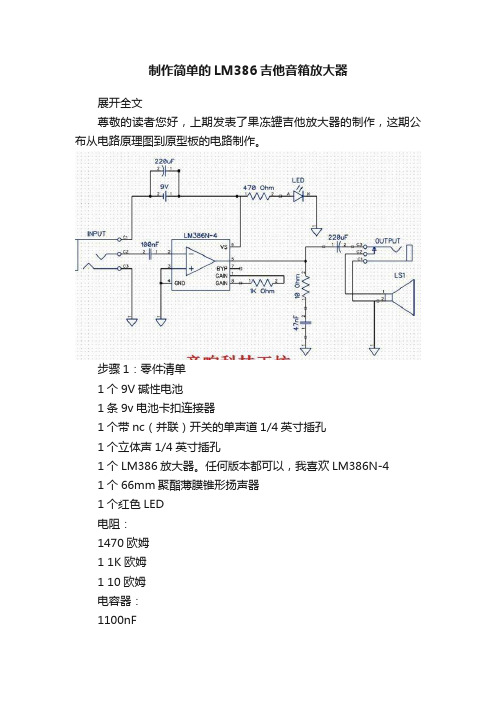
制作简单的LM386吉他音箱放大器展开全文尊敬的读者您好,上期发表了果冻罐吉他放大器的制作,这期公布从电路原理图到原型板的电路制作。
步骤1:零件清单1个9V碱性电池1条9v电池卡扣连接器1个带nc(并联)开关的单声道1/4英寸插孔1个立体声1/4英寸插孔1个LM386放大器。
任何版本都可以,我喜欢LM386N-41个66mm聚酯薄膜锥形扬声器1个红色LED电阻:1470欧姆1 1K欧姆1 10欧姆电容器:1100nF1 47nF2220uF洞洞板烙铁和焊锡步骤2:洞洞板这种洞洞板是为集成电路制作的,方便引线和焊接。
零件都含在没有铜箔的一面。
最好是先规划一下,免得走线混乱引起错误。
步骤3:将原理图转换为原型板因此,一旦您设计好电路并制作了原理图,就可以开始研究原型板的布局了。
您将铅笔拿到纸上,然后开始在protoboard插图上布置组件。
这需要一些技巧。
需要一些时间。
这将花费大量的纸张。
在上方,您可以看到原理图和原型板上的成品轮廓。
计划原型板上的组件位置时,我会分阶段进行计划。
我将从芯片的放置开始。
我从左到右工作,所以我将布局如下:输入---- IC芯片----输出该电路的输入非常简单,因此芯片将放置在原型板的左侧。
这为输出组件留出了空间。
下一步是布置电路的所有电源。
下一步是布置输入和输出组件。
下一步是添加增益组件和LED电源指示灯下一步是添加外围组件,例如输入和输出插孔。
每个阶段都建立在最后一个阶段。
从最简单到更复杂。
分阶段进行构建可以使您在进行过程中进行测试和故障排除,以便在出现错误的情况下更早发现并可以将其与构建中的先前阶段隔离开来。
将原理图转换为原型板图之后,就该构建真正的电路了。
我将原型板图分解成几张纸,每张纸都包含一个阶段或构建的一部分。
因此,我可以打印出构建的每个部分,并在进行过程中检查放置在真实原型板上的组件,以确保没有遗漏任何东西。
这对于复杂的构建尤其重要。
对于此特定电路,我们将分4部分进行构建。
LM3886中文资料

M3886中文资料概述M3886TF是美国NS公司推出的新型的大功率音频放大集成电路,其后面的TF为全绝缘封装,和 LM1875T相比,它的功率较大,在额定工作电压下最大可达68W的连续不失真平均功率,同样具有比较完善的过压过流过热保护功能,最可贵的是它具有自动抗开关机时的电流冲击的功能,使扬声器能够安全的工作。
LM3886优异的性能,使得它在近几年音响制作中广泛的应用,许多成品功放机中就有直接的应用它担任后级功放或者用它作为重低音放大电路。
采用了美国N S公司(国家半导体公司)推出的新型高保真音响功放集成电路LM3 886TF作功率放大,用运放NE5532或AD827作前置线性放大和音调放大。
其特点有:输出功率大(连续输出功率68W)、失真度小(总失真加噪声<003%)、保护功能(包括过压保护、过热保护、电流限制、温度限制、开关电源时的扬声器冲击保护、静噪功能)齐全,外围元件少,制作调试容易,工作稳定可靠。
由于用它制作功率放大电路具有简易,适用的特点,特别适合于烧友以及电子爱好者的制作。
电气参数LM3886TF在VCC=VEE=28V、 4欧负载时能达到68W的连续平均功率,在VCC=VEE=35V,8欧负载时能达到50W的平均功率。
具有较宽的电源电压范围VCC+VEE为20V-94V;总谐波失真+噪声:60W 20Hz<F;转换速率(SLEW RATE):VIN=2.0VP-P、tRISE=2ns 时的值为 19V /us总静态电流:50mA输入偏流:0.2uA增益带宽乘积: 8 MHZ内部电路图应用电路(1)应用电路LM3886带过压、过高温保护并且具有静噪功能的68W单声道高保真功率放大器,其主要电气参数如表所示。
LM3886采用11脚TO-220封装。
LM3886典型应用电路如图3所示。
LM3886在供电电压为。
10V以上时即可工作,只是输出功率降低。
IM3886的⑧脚为静音控制端,当流过该脚的电流大于1mA时,输出电路执行静音操作,输出端无信号输出。
lm386-电路原理---音频放大器

lm386-电路原理---音频放大器
lm386是一种常用的音频放大器,适用于低功率音响系统和电子设备。
它的特点是简
单易懂,工作可靠,价格低廉,在DIY音响的世界中广泛应用。
那么,它的电路原理是什
么呢?
lm386的电路原理可以简单地分为两部分,输入放大器和输出放大器。
输入放大器:
输入放大器是一种放大器电路,把输入信号的电压放大,输出电压变成一个更高的信号,经过一个低通滤波器后去除高频噪声。
在lm386中,输入信号通过C1电容进入放大器,并且经过R1和R2电阻分压降低信号电平。
接着信号通过放大器U1的非反向输入端,通过R3电阻形成负反馈,使放大器的放大倍数稳定,同时降低了噪声。
输出放大器将放大后的信号通过一个大功率晶体管输出到喇叭,将电信号转换成声音。
在lm386中,输出放大器也采用负反馈控制的方式,控制输出电压,稳定功率。
U1的输出通过C4电容进入输出级别放大器,驱动晶体管Q1的基极。
经过高通滤波器C8,将基极引到电源电压的一半,同时降低直流偏置。
晶体管Q1的输出将声音发出,同时反馈到放大器的非反向输入。
总体来说,lm386基本是一个放大器电路,通过输入和输出放大器的组合,可以实现
低功率的音频放大。
除了基本的电路原理,还可以结合其他元件组合出多种不同的效果,
如有源音量控制、三合一音量控制、失真音效等等。
从硬件上选择经典的 lm386芯片,再结合趣味DIY的组合美学,很容易得出简单、实用和覆盖大部分音响需求的二合一放大器
方案。
- 1、下载文档前请自行甄别文档内容的完整性,平台不提供额外的编辑、内容补充、找答案等附加服务。
- 2、"仅部分预览"的文档,不可在线预览部分如存在完整性等问题,可反馈申请退款(可完整预览的文档不适用该条件!)。
- 3、如文档侵犯您的权益,请联系客服反馈,我们会尽快为您处理(人工客服工作时间:9:00-18:30)。
使用LM3886制作的低音炮电路图
作者:低音之父来源:未知日期:2009-10-19 14:24:04 人气:4566 标签:
导读:LM3886TF是美国NS公司推出的新型的大功率音频放大集成电路,其后面的TF为全绝缘封装,和L M1875T相比,它的功率较大,在额定工作电压下最大可达68W的连续不失真
LM3886TF是美国NS公司推出的新型的大功率音频放大集成电路,其后面的TF为全绝缘封装,和 LM1875T相比,它的功率较大,在额定工作电压下最大可达68W的连续不失真平均功率,同样具有比较完善的过压过流过热保护功能,最可贵的是它具有自动抗开关机时的电流冲击的功能,使扬声器能够安全的工作。
LM3886优异的性能,使得它在近几年音响制作中广泛的应用,许多成品功放机中就有直接的应用它担任后级功放或者用它作为重低音放大电路。
采用了美国NS公司(国家半导体公司)推出的新型高保真音响功放集成电路LM 3886TF作功率放大,用运放NE5532或AD827作前置线性放大和音调放大。
其特点有:输出功率大(连续输出功率68W)、失真度小(总失真加噪声<0 03%)、保护功能(包括过压保护、过热保护、电流限制、温度限制、开关电源时的扬声器冲击保护、静噪功能)齐全,外围元件少,制作调试容易,工作稳定可靠。
由于用它制作功率放大电路具有简易,适用的特点,特别适合于烧友以及电子爱好者的制作。
LM3886TF的电气参数如下:
LM3886在VCC=VEE=28V、 4欧负载时能达到68W的连续平均功率,在VCC=VEE=35V,8欧负载时能达到50W的平均功率。
具有较宽的电源电压范围VCC+VEE为20V-94V;
总谐波失真+噪声:60W 20Hz<F
转换速率(SLEW RATE):VIN=2.0VP-P、tRISE=2ns 时的值为 19V/us
总静态电流:50mA
输入偏流: 0.2uA
增益带宽乘积: 8 MHZ
LM3886各脚位定义
LM3886典型应用电路
LM3886实际应用电路一例。