Virtuoso Layout Editor
layout快捷键

Cadence版图布局软件Virtuso Layout Editor快捷键归纳:单击左键选中一个图形(如果是两个图形交叠的话,单击左键选中其中一个图形,在单击选中另一个图形)用左键框选,选中一片图形,某个图形要被完全包围才会被选中。
中键单击调出常用菜单命令(很少用,要点两下,麻烦。
我们有快捷键的嘛)右键点击拖放用来放大。
放大后经常配合F键使用,恢复到全部显示。
配合Tab键使用,平移视图。
右键还有“Strokes”,就是点住右键画些图线,就能实现调用某些命令。
Shift+左键加选图形,Ctrl+左键减选图形。
(Cadence菜单中大写表示+按shift,Ctrl写成^)F1 显示帮助窗口。
F2 保存。
F3 这个快捷键很有用,是控制在选取相应工具后是否显示相应属性对话框的。
比如在选取Path工具后,想控制Path的走向,可以按F3调出对话框进行设置。
F4 英文是Toggle Partial Select,就是用来控制是否可以部分选择一个图形。
F5 打开。
F6,F7帮助上有,但我试过,没反应-_-F8 Guided Path Create 切换至L90XYFirst。
F9 是Filter Size 我不知道怎么用。
Ctrl+A 全选。
这个和windows下是一样的。
Shift+B Return。
这个牵扯到“Hierarchy”。
我翻译成“等级”。
这个命令就是等级升一级,升到上一级视图。
B键去某一级(Go to Level)。
Ctrl+C 中断某个命令,不常用。
一般多按几次Esc键取消某个命令。
Shift+C 裁切(Chop)。
首先调用命令,选中要裁切的图形,后画矩形裁切。
C键复制。
复制某个图形。
Ctrl +D 取消选择。
这个也可用鼠标点击空白区域实现。
这个快捷键和Photoshop中的取消选区的快捷键是一样的。
还有Shift+D,和D也是取消选择,我觉得很不实用。
Shift+E和E是控制用户预设的一些选项。
Virtuoso Layout Editor
安装Pcell
第八步:把上面定义的内容存入工艺文件
最后按OK完 成安装!
版图编辑,按i键
使用Pcell
增加的 Pcells
使用Pcell
利用Pcell生成 W=5u; L=0.6u M=2 的PMOS管
使用Pcell
Flatten Pcell 后,pcell就 被打散为各 个部分,在 此基础上对 其进行加工, 可得到一些 不规则的版 图设计
注意大小写不要弄错!
快捷方法:选中并 ctrl+c,然后在CIW中点 击中键,就可以把复制的内容粘贴过去,最 后回车
安装Pcell
下一步,ok则终止安装
Welcome Window 继续前阅读这部分 内容
安装Pcell
第一步:选择要 安装的Devices
这里只选择了最常用的 nmos/pmos,你也可以同时选 上其他选项,大家可回去练习
安装Pcell
第四步:确定设计规则
自动弹出规则定 义窗口,根据设 计规则分别设定 各项值,然后按 OK,在第四步 窗口按next
安装Pcell
第五步:直接点击next
安装Pcell
第六步:提示找到安装devices所 需的文件,直接点击next
安装Pcell
第七步:依照默认选项, 直接点击next
Name: pguardring 改为 nguardring
在pguardring的基础上 修改生成nguardring
Multipart paths
删去subpath: pimp,添加 subpath: nimp
Multipart paths
将nguardring的定义存入工艺文件
Multipart paths
VLE(virtuosoLayoutEditing)快捷键
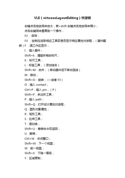
VLE(virtuosoLayoutEditing)快捷键右键点击拖放用来放大,若+shift右键点击拖放用来缩小;点击右键用来重复前一个操作;F2 :保存;F3 :控制在选取相应工具后是否显示相应属性对话框;(器件翻转)F :满工作区显示;I :插入器件;Shift+k:清楚所有的标尺;K:标尺工具;L:标签工具;(添加线名)Shift+M:合并;(移动器件但不移动连线)M:移动;Shift+O:旋转;(r或者F3)O:插入contact;Ctrl+P:插入pin;(P)Shift+P:多边形工具;P:插入path;Shift+Q:打开设计属性对话框;Q:图形对象属性;R:矩形工具;S:拉伸工具;T:层切换;Shift+U:撤销命令后返回;U:撤销;Ctrl+W:关闭窗口;Shift+W:下一个视图;W:前一视图;Shift+X:下降一等级;Y:区域复制;Ctrl+Z:放大两倍;Shift+Z:缩小两倍;Z:放大;ESC:取消;Tab:平移视图;Backspace:撤销上一点;Enter:确定一个图形的最后一点,也可双击鼠标左键结束;Shift+F:显示所有等级,ctrl+F:显示上一等级;Ctrl+N :先横后竖。
L90XFirst ;Shift+N :直角正交。
Orthogonal;(添加标号)N :斜45对角+正交Diagonal;(添加几何图形)V:关联attach;Ctrl+D:取消选择,也可用鼠标点击空白部分实现;Shift+C:裁切,首先调用命令,选中要裁切的图形,后画矩形裁切;Shift+l:标注;g:查看错误;shift+e:查看底层电路;ctrl+e:返回顶层电路;e:进入内部电路;。
Cadence版图布局软件Virtuso Layout Editor快捷键归纳
Cadence版图布局软件Virtuso Layout Editor快捷键归纳[zz]摘自首先介绍下鼠标操作吧。
单击左键选中一个图形(如果是两个图形交叠的话,单击左键选中其中一个图形,在单击选中另一个图形)用左键框选,选中一片图形,某个图形要被完全包围才会被选中。
中键单击调出常用菜单命令(很少用,要点两下,麻烦。
我们有快捷键的嘛)右键点击拖放用来放大。
放大后经常配合F键使用,恢复到全部显示。
配合Tab 键使用,平移视图。
右键还有“Strokes”,就是点住右键画些图线,就能实现调用某些命令。
Shift+左键加选图形,Ctrl+左键减选图形。
(Cadence菜单中大写表示+按shift,Ctrl写成^)F1 显示帮助窗口。
F2 保存。
F3 这个快捷键很有用,是控制在选取相应工具后是否显示相应属性对话框的。
比如在选取Path工具后,想控制Path的走向,可以按F3调出对话框进行设置。
F4 英文是Toggle Partial Select,就是用来控制是否可以部分选择一个图形。
F5 打开。
F6,F7帮助上有,但我试过,没反应-_-!!!F8 Guided Path Create 切换至L90XYFirst。
F9 是Filter Size 我不知道怎么用。
Ctrl+A 全选。
这个和windows下是一样的。
Shift+B Return。
这个牵扯到“Hierarchy”。
我翻译成“等级”。
这个命令就是等级升一级,升到上一级视图。
B键去某一级(Go to Level)。
Ctrl+C 中断某个命令,不常用。
一般多按几次Esc键取消某个命令。
Shift+C 裁切(Chop)。
首先调用命令,选中要裁切的图形,后画矩形裁切。
C键复制。
复制某个图形。
Ctrl +D 取消选择。
这个也可用鼠标点击空白区域实现。
这个快捷键和Photoshop中的取消选区的快捷键是一样的。
还有Shift+D,和D也是取消选择,我觉得很不实用。
Virtuoso Layout Editing Introduction
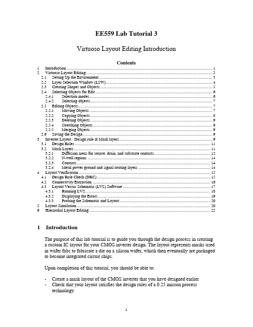
EE559 Lab Tutorial 3Virtuoso Layout Editing IntroductionContents1Introduction (1)2Virtuoso Layout Editing (2)2.1Setting Up the Environment (3)2.2Layer Selection Window (LSW) (4)2.3Creating Shapes and Objects (5)2.4Selecting Objects for Edit (6)2.4.1Selection modes (6)2.4.2Selecting objects (7)2.5Editing Objects (7)2.5.1Moving Objects (7)2.5.2Copying Objects (8)2.5.3Deleting Objects (9)2.5.4Stretching Objects (9)2.5.5Merging Objects (9)2.6Saving the Design (9)3Inverter Layout : Design rule & Mask layers (9)3.1Design Rules (11)3.2Mask Layers (11)3.2.1Diffusion areas for source, drain, and substrate contacts (12)3.2.2N-well regions (14)3.2.3Contacts (14)3.2.4Metal power ground and signal routing layers (14)4Layout Verification (15)4.1Design Rule Check (DRC) (15)4.2Connectivity Extraction (16)4.3Layout Versus Schematic (LVS) Software (17)4.3.1Running LVS (18)4.3.2Displaying the Errors (19)4.3.3Probing the Schematic and Layout (20)5Layout Simulation (20)6Hierarchal Layout Editing (22)1IntroductionThe purpose of this lab tutorial is to guide you through the design process in creatinga custom IC layout for your CMOS inverter design. The layout represents masks usedin wafer fabs to fabricate a die on a silicon wafer, which then eventually are packaged to become integrated circuit chips.Upon completion of this tutorial, you should be able to:-Create a mask layout of the CMOS inverter that you have designed earlier-Check that your layout satisfies the design rules of a 0.25 micron process technology-Check that your layout passes the automatic verification against that inverter schematic created earlier-Extract a netlist including parasitic resistances and capacitances from the layout -Simulate the netlist using HSPICE or Nanosim, and compare results to schematic simulations done earlier•The format of this tutorial is not providing step by step instruction to complete the layout design and verification but it contains enough explanations to help you tofinish the basic design work.•More information about the layout tool can be found in the online documentation under the Layout Editor (cdsdoc command).•For the evaluation, you need to generate DRC/LVS error free layout of inverter and InverterTest design and do the layout simulationsuccessfully. When you do the layout simulation, use the input signal pattern that you used in the schematic simulation.2Virtuoso Layout Editing•Before you begin running the layout editor, copy the display.drf file from the /package/eda/cells/tsmc025/ directory to your home directory •To start up the Virtuoso Layout Editor, enter layoutPlus in a UNIX window prompt (note the uppercase “P”). You can also use icfb instead oflayoutPlus. The Main difference is that layoutPlus doesn’t provide thesimulation functionality.•When the CIW appears, select File -› New -› Cellview. Similarly, you can use the Library Manager to create new cellviews. In the new window that appears, setLibrary Name to tutorial and type in inverter as the Cell Name. In the ViewName field, type in layout and press the tab key. The Tool field should change to Virtuoso. Click OK to continue.•Two windows will appear. One is called the Layer Selection Window (LSW). The LSW allows you to choose the layer on which you create objects, set which layers are selectable and set layer visibility. Note that the technology file that youentered in the first tutorial (cmosp25) defines the layers and colors that will beavailable to you in the LSW.•The other window is the layout window (Virtuoso Layout Editing) where you perform the place and route of the inverter layout.2.1 Setting Up the EnvironmentBefore you start doing your layout, you need to setup the grid size of the cellview so that each grid will correspond to a dimension that will make the layout process easier and allow for a more compact design.•To set up the display environment, select Options -› Display. The Display Option window will appear. In the window, change Minor Spacing to 0.06 and MajorSpacing to 0.30. Change both X Snap Spacing and Y Snap Spacing to 0.02.•Leave other settings at their default setting. However, take note that those options will allow you to change the display of the cellview if need arises. Please refer to the online documentation if you need further information.•The settings can be saved and loaded back using the Save To and Load From buttons at the bottom of the window. You can choose to save or load settings toeither the cellview, library of the cellview, technology of the cellview, or aspecified file. If you are saving to a file, the settings from both the Layout Editor Options and Display Options windows will be saved. Click OK when done.•Back in the layout window, select Options -› Layout Editor. The Layout Editor Option window will appear. Options here allow you to change the editingcommands of the editor and change how the cursor behaves.•In the Layout Editor Option window, uncheck the Gravity On box. This will prevent the cursor from being “attracted” to other objects already drawn in thecellview. Experiment on your own. If you feel that you are comfortable with this function or find it useful in certain situations, you can turn it on. Click OK when done.2.2 Layer Selection Window (LSW)The Layer Selection Window (LSW) lets you to choose the layer on which you create objects (called the entry layer). It also controls which layers are selectable or visible.•To change the LSW to make layers selectable or visible, move the cursor over the layer and click using the middle button. It will toggle layer visibility and alsoautomatically sets invisible layers to be unselectable. The text layer colordisappears to show the layer is invisible. The layer name turns gray to show thelayer is not selectable.•Every time after you have selected the layer, select Window -› Redraw to see the effect of any LSW changes that you have made. This will allow you to makeseveral changes in the LSW before taking time to redraw the cellview, especially in complex designs.•To make the layers visible, click on the AV (All Visible) button. The colored squares showing the layer color reappear, and the shading on the layer namedisappears.•Use the left mouse button to select layers for entry in the LSW. The abbreviation dg after each layer name means drawing (pn means pin).2.3 Creating Shapes and ObjectsMost of the layers that you will draw will be rectangles or polygons that arerectilinear in shape. The sizes of the objects depend on the design and the design rules.Creating rectangles•To create rectangles, select a layer (for example, metal1/dg) from the LSW, then select Create -› Rectangle or click the Rectangle icon on the left. In the newwindow that appears, type the net name you want the rectangle to be associatedwith. You can choose to leave it blank and name the net later. Shortkey forcreating rectangles is ‘r’•Note that assigning names to the nets aid in the future layout verification processes. However, ensure that the net names on the layout matches the ones inthe schematic, otherwise the LVS program (refer to section 4.3) will fail to match the nets.•Point and click on the first corner of the rectangle, then point to the opposite corner of the rectangle (follow the prompt in the layout window and CIW).Creating polygons•Another way of creating objects is to create polygons. Select a layer from the LSW, then select Create -› Polygon or click the Polygon icon on the left. In thenew window that appears, type the net name you want the polygon to beassociated with. You can choose to leave it blank and name the net later. Set Snap Mode to orthogonal. The snap mode controls the way segments snap to thedrawing grid as you create the polygon by placing its vertices.•Point and click on the first point of the polygon. The CIW will prompt for the second point of the polygon. Move the cursor to click on a second point. Thelayout editor will create a solid line parallel to either the Y-axis or the X-axis.Continue to click on a third point that is orthogonal to the solid line. The layouteditor will create two solid lines at right angles to each other between the pointsyou entered. You will also see two dashed lines at right angles to each otherattached to the two points you entered. The dashed lines show how the layouteditor would finish the polygon if you click twice on this point you entered.•If you made a mistake in one of the points while creating the polygon, you can hit the Backspace key to undo them in order.Creating Pins•In order to perform layout verification after the layout is completed (refer to section 4.0), pins must be created to match the schematic.•To create pins, select Create -› Pin. In the window that appears, change the Mode to shape pin. A new window named Create Shape Pin will replace the previouswindow.•Enter the pin net name in the Terminal Names field. Make sure that the names exactly match the schematic (case sensitive). If you are not sure about the names of the pin nets, open the schematic and check the net properties.•Turn on the Display Pin Name option if you would like the pin names to be displayed on the layout cellview. Click the Display Pin Name Option button tochange the display properties of the pin names (size, font, direction etc.).•Select the I/O Type accordingly. For power and ground pins, select inputOutput.•Select the layer in the LSW (use the layer that has the pn abbreviation) and draw the pin in the cellview by clicking on one corner of the pin, followed by thesecond corner.•If you have chosen to display the pin name in the cellview, after you have placed the second corner of the pin, the pin name will appear next to cursor. Move thecursor to where you want the pin name placed and click.2.4 Selecting Objects for Edit2.4.1 Selection modesTo edit an object, first you need to select it. There are two selection modes: full and partial. Press the F4 key to toggle between selection modes and the mode is displayed in the status banner of the layout window (top).•In full selection mode (default), you select the entire object when it is clicked.When in full mode, the status banner will display:(F) Select: 0•In partial selection mode, you can select the entire object or just edge or corner of an object. When in partial mode, the status banner will display:(P) Select: 02.4.2 Selecting objects•To select an object, set the selection mode and click the object.•To deselect all objects, click in an empty part of the design.•To select one or several objects at a time, press the Shift key while selecting.•To deselect one or several objects after they have been selected, press the Ctrl key and select.2.5 Editing ObjectsThere are several functions that are commonly used to edit objects. They include: move, copy, delete, stretch and merge. Should you require more advanced editing methods, please refer to the Editing Objects section in the Virtuoso Layout Editor User Guide.2.5.1 Moving Objects•To move an object, change to full selection mode and select the object(s). Notice that when you move the cursor within the selected object, the pointer changes tofour arrows. This indicates that the object(s) can be moved by clicking anddragging.•Alternatively, you can choose to select Edit -› Move from the drop down menu or use the Move icon on the left. The Move window appears. After you have selectedthe object(s), the CIW will prompt you for a reference point (start point) for themove. Click on the reference point for the move, and drag the pointer to thedestination point. The object will be moved with respect to the reference point.•Note that in the Move window, there is a Change To Layer option. This will allow you to move and change the object from one layer to another without having toredraw the object. Check the box to enable the Change To Layer function andmove the object as usual.•You can rotate or flip the object (sideways or upside down) by clicking the Rotate, Sideways and Upside Down buttons in the Move window before placing the object. You can also do the same by using the right click on the mouse afteryou have selected the reference point for the move. Shortkey for move function is ‘m’.2.5.2 Copying Objects•To copy an object, select Edit -› Copy or use the Copy icon after you have selected the object(s). After the copy window appears, select the object(s) to becopied. The CIW will prompt you for a reference point (start point) for the copy.Click on the reference point for the copy, and drag the pointer to the destinationpoint. The object will be copied with respect to the reference point. Shortkey forcopy function is ‘c’.•To copy and paste multiple copies of the object, type in the number of copies in either the Rows or Columns fields and place the objects in the cellview as usual.•To copy and paste an array of copied objects, enter both rows and columns. The CIW will prompt you to place the first object of the array. After you have placedthe first object, continue to place the second column of the array. The distancebetween the first object and the second will determine the spacing and orientation between the rest of the columns. After you have placed the columns, click to place the rows of the array and complete the array. Similarly, the distance between thefirst and second rows will determine the spacing and orientation between the rest of the rows.•Note that in the Copy window, there is a Change To Layer option. This will allow you to copy and change the object from one layer to another without having toredraw the object. Check the box to enable the Change To Layer function andcopy the object as usual.•You can rotate or flip the object (sideways or upside down) by clicking the Rotate, Sideways and Upside Down buttons in the Copy window before placingthe object. You can also do the same by using the right click on the mouse afteryou have selected the reference point for the move2.5.3 Deleting Objects•To delete an object, change to full selection mode and select the object(s). Select Edit -› Delete or press the Delete key.2.5.4 Stretching Objects•To stretch an object, switch to partial selection mode and select the object(s) at its corners and edges. Notice that when you move the cursor within the selectedobject, the pointer changes to an arrow pointing to a line. This indicates that theobject(s) can be stretched at the corners or edges by clicking and dragging.•Alternatively, you can choose to select Edit -› Stretch from the drop down menu or use the Stretch icon on the left. The Stretch window appears. Leave the LockAngles option on unless you need to form nonorthogonal shapes. After you haveselected the edge(s) to be stretched, the CIW will prompt you for a reference point (start point) for the stretch. Click on the reference point for the stretch, and dragthe pointer to the destination point. The object will be stretched with respect to the reference point. Shortkey for stretch function is ‘s’.2.5.5 Merging Objects•You can use the merge function to merge two objects of the same layer. To merge objects, select the objects to be merged, then select Edit -› Merge.2.6 Saving the Design•To save the design, select Design -› Save or click the Save icon on the left.3 Inverter Layout : Design rule & Mask layersThe pictures in this section present an inverter layout very similar to the one you are about to create. The only significant difference should be the transistor widths. The inverter you create should have transistor widths matching the values you determined in tutorial 1.This layout is in the style of standard cells used for automated placement and routing of random logic. This does not, however, mean that this style of layout is bad for custom layout. It has some very useful features. In particular,•It is designed so that multiple instances of the cell can be connected together by abutment (i.e., placed immediately to the left and right of each other). The power, ground, input, and output connections line up and will be connected. Of course, you may wish to have the input and output not line up so that you can have the power and ground connections connect up without necessarily connecting the input and output together.•The layout lends itself to a left to right signal flow in the metal layer (used for the input and output) as well as vertical signal flow for short distances in polysilicon. •If other types of logic cells have the same layout spacing between power and ground, then cells of various types can be chained together easily.3.1 Design Rules•Design rules are a set of rules (usually supplied by the manufacturer) that specifya minimum size or spacing requirements between layers of the same type or ofdifferent types. This provides a safety margin for various process variations, toensure that your design will still have reasonable performance after your circuit is fabricated.•Note that the technology file you specified in the first tutorial (cmosp25) defines the design rules that will be used to check your design. It also defines how thedrawing layers are translated into masks for the IC. The design rule file used isdivaDRC.rul.•The following section will discuss about the more common design rules. For other design rules, they can be found in the T-025-MM-DR-002.pdf file in the/package/eda/cells/tsmc025 directory.3.2 Mask LayersThe mask layers are the various layers shown in the above diagram and are used to define the location and size of the devices and nets. Each layer can be treated as an individual layer meaning that two different layers have no electrical connectionbetween them even though they happen to overlap. The layers are typically indifferent colors and shading (displayed in the Layer Selection Window – refer tosection 3.2) and are defined by the display.drf file.3.2.1 Diffusion areas for source, drain, and substrate contacts•Rectangles on the active layer are used to define the region where doping is to be applied (except under the polysilicon gate) to form the source and drain of eachtransistor. For an NMOS transistor, the doping will be n+. For a PMOS transistor, this doping will be p+. It will be shown later how the type of doping is actuallyspecified.•Rectangles on the poly1 layer are used to define the strips of polysilicon used to form the gate of each transistor and to provide short distance connections between transistors in the inverter.•The intersection of an active and poly1 region defines the channel of a transistor.Since the minimum size of active is 0.30μ and poly1 is 0.24μ, this means that the minimum transistor width must be 0.30μ and the minimum length must be 0.24μ.•Note that in some cases, it may not be possible to draw an active area as a simple rectangle. The area may have to be one width at the source and drain toaccommodate the required clearance around source and drain contacts. It thenmay need to be notched to obtain the necessary transistor width for theintersection with poly1.•The active layer is also used to define regions that must be doped to allow a bulk (substrate or well) contact. In p- substrate, the doping must be p+ type. In an N-well (where PMOS transistors are placed), the doping must be n+ type. Note that there are square active layers in the above inverter layout example to form thebulk contacts.•Rectangles on the nplus and pplus layers are used to control the type of dopant applied to each diffusion area. Note that these areas must extend past the diffusion area (active) by at least 0.26μ.Figure 3.3. NMOS and PMOS transistorsFigure 3.4. N-well contact for PMOSFigure 3.5. P-substrate contact for NMOS3.2.2 N-well regions•PMOS transistors must be located in substrate with N type doping. The substrate for the PMOS transistors is formed by diffusing N type dopant into regions of the normally p- type substrate. Rectangles in the nwell layer define these regions inwhich PMOS transistors can be placed.3.2.3 Contacts•0.30μ x 0.30μ squares drawn on the contact layer will cause metal plugs to be placed into contact with the diffusion areas to form source, drain, and substrate or well contacts.•0.30μ x 0.30μ squares drawn on the contact layer will cause metal plugs to be placed into contact with the poly1 areas to form poly contacts.•Metal placed on layer metal1 will connect with these contacts.3.2.4 Metal power ground and signal routing layers•Rectangles on the metal1 layer define regions of aluminum to be placed in the first metal layer. In this case metal1 is used for all inputs and outputs to theinverter.• A 0.30μ x 0.30μ square on contact provides a metal plug to connect routing on layer metal1 to polysilicon routing below on the poly1 layer.•In the 0.24μ TSMC process, there are several other metal layers available (metal2, metal3 and so on). We are not going to use it in this layout since it is not needed. However, in larger more complex layouts, both layers will be needed.Often it is a wise practice to route all signals horizontally on one layer andvertically on another layer.•To connect the metal1 layer to the metal2 layer, a square on via12 is used.•You can connect other metal layers together using the appropriate via layers. For example, to connect the metal2 layer to the metal3 layer, a square on via23 isused.4 Layout VerificationAfter you have completed the layout, you need to perform several verificationprocedures to ensure that the layout does not violate any design rules and doesactually correspond with the schematic design that you have made earlier.4.1 Design Rule Check (DRC)DRC checks your layout against physical design rules defined in the divaDRC.rul file. It will display error information if it finds any part in the layout that violates the design rules. Note that this is only a physical design check and does not verify the actual performance or functionality of the layout design.•To run DRC, select Verify -› DRC from the drop down menu. Check that the Rules file and the Rules library fields are correct in the DRC window. Click OKto start.•If there are any errors, it will be reported in the CIW. A blinking polygon, called an error marker, appears in the cellview at the location of the error.•To view the errors and get a brief description of the error, select Verify-> Markers -› Explain and click on any error marker. The marker will behighlighted in yellow to indicate that it is selected. A window named marker textwill appear that contains information about the cellview that contains the errorand the rule that was violated.•To quit the Explain command, press the Esc key.•To remove the markers, select Verify -› Markers-› Delete All. The Delete All Markers window appears. Click OK to remove the markers.•If any errors are reported, make changes to the layout and re-run DRC until all errors have been fixed.•For large complex designs, it is possible to run an incremental DRC. This means that the system will keep track of any changes you made since the last DRC and it will check only the changes made. This will make DRC run faster as it does nothave to re-check every part of the design.•To turn on incremental DRC, set the Checking Limit to incremental in the DRC window.•It is also possible to run a DRC on a specific area. To do this, set the Checking Limit to area in the DRC window, and click on the Sel by Cursor button. Selectthe area on the cellview that you want a DRC to be performed on by clicking onthe first point of the rectangle followed by the second point. The coordinates ofthe points will be entered.4.2 Connectivity ExtractionBefore performing a Layout Versus Schematic (LVS) check, you need to extract the connectivity form the layout cellview by running the Extract program. The Extract program uses rules defined in the technology file to recognize devices and establish electrical connections or nets. It will create an extracted cellview that shows the nets.•To run the Extract program, select Verify -› Extract.•In the Extractor window, select flat as the Extract Method. A flat extract method is used because parasitic capacitance values can vary between different instances of the same cell, thus each cell must be extracted.•Turn on Join Nets With Same Name. This will merge nets with the same names while suppressing warning messages about different nets that have the samename.•To select the types of parasitics that are to be extracted, click the Set Switches button in the Extractor window. In the Set Switches window that appears, selectthe type of parasitics that are to be extracted (typically parasitic capacitances).Click OK when done selecting.•Click OK or Apply in the Extractor window to create the extracted views.•The extraction rules appear in the CIW as the extract program executes. When the extraction is complete, a message saying that the extracted cellview is saved will be shown.•To view the extracted cellview, select File -› Open from the CIW. It should be under the same library and cell name. Select the extracted view name and clickOK.•The extracted cellview appears on top of the layout cellview. Notice that the extracted cellview is similar to the layout, but the gates now have symbols at one end. Displayed next to the symbols are the gate width and length.•To display the electrical connections, open the Display Options window and select Nets. Click Apply when done.4.3 Layout Versus Schematic (LVS) SoftwareAs its name implies, the LVS program performs a comparison of the schematic to the physical layout. It will use both the extracted view and the schematic view of the layout. If you did not create an extracted view, LVS will not work.4.3.1 Running LVS•To run LVS, select Verify -› LVS.•If a LVS Form Contents Different window appears, click OK to continue.•In the LVS window, fill in the schematic and extracted fields either with the Browse or Sel by Cursor button. If you choose to use the Sel by Cursor button, click on the button, then simply click in any area of the schematic or extractedcellview window.•Note that if both the schematic and extracted cellview are opened before the LVS window, the fields should already be filled automatically. Check to ensure thatthey are correct.•Make sure that the specified Rules File is divaLVS.rul and the Rules Library is cmosp25.•Turn off the Correspondence File option. The purpose of the correspondence file is to allow the user to identify schematic/layout nodes that should be mappedto each other. Mainly you would do this if LVS has trouble matchingthe schematic and layout on its own.•Click Run to start LVS. When the Save Cellview window appears, click OK to save. The LVS job runs in the background and might take a couple of minutes to complete, depending on the complexity of the design. When the job is finished, a dialog box named Analysis Job Succeeded will appear. Note that this only meansthat the LVS program was executed successfully and does not mean that thelayout matches the schematic.•To view the LVS results, click Output in the LVS window. A text window listing the output from the LVS run appears. Scroll down until the section that compares the layout and schematic is displayed. In that section, it will report whether thetwo designs match and provide a list of the numbers of instances and nets.If LVS verifies that the layout matches the schematic, it will report:The net-lists matchOtherwise, it would report:The net-lists failed to match•If the layout fails to match the schematic, the errors on the layout must be corrected.4.3.2 Displaying the Errors•Make sure that the extracted cellview is opened before you continue.•To display the errors, click the Error Display button at the bottom of the LVS window.•In the LVS Error Display window that appears, click the First button in the Display field. The error message will be displayed below the Display field. Inaddition, the geometries in the extracted layout that do not match anything in the schematic will be highlighted in a color specified in the Error Color field.•You can check the Auto Zoom option to zoom to the error. To clear the markers, click on the Clear Display button in the LVS Error Display window.。
利用Cadence virtuoso layout edit制做pcell 芯片版图
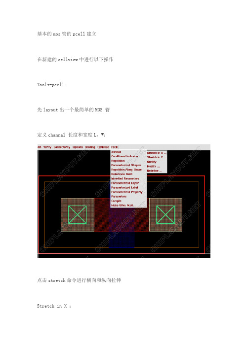
基本的mos管的pcell建立在新建的cellview中进行以下操作Tools-pcell先layout出一个最简单的MOS 管定义channal 长度和宽度L,W:点击stretch命令进行横向和纵向拉伸Stretch in X :将出现的控制线,跨过你所需要拉伸的所有layer,然后按enter出现下图所示的图框Name or Expression for stretch:自己取个名字,比如L代表了channal channelReference Dimension (Default):L的尺寸,默认为控制线所经过的最小layer 宽度其他的几个选项可以调整layer 拉伸的方向和最小最大值W用stretch in Y定义然后看看成果点击compile –to pcell,进行编辑点击OK,并且保存。
可以看到现在调用出来的MOS 已经是一个可以编辑W,L的器件了。
但是我们有的时候我们要用到多个finger并联,所以可以通过设置另外一个参数M来实现。
因为M实际上就是一个finger复制M次,所以我们要用到repetition选项,如果这样直接使用这个操作,无法实现我们需要的结果,现在进行repetition的L是原始的L但是希望得到的是L改变后的复制,所以我们用到stretch-qualify点击Qualify,此时控制线可选,点击控制L的线,并希望与其一起变化的layer,并双击或者enter确定现在就可以进行repetition操作了。
我们还需要定义一个X方向的辅助参数ods,选中需要repeatlayer,一般是poly,contact,metal,Repetition-repeat in X,Ok,然后进行compile-to pcell同样的方法不用定义ods,然后其他定义和上相同,调用两个pcell可以看出两者的不同横向的repeat后,要进行纵向的repeat一般选择contact repeat。
关于Cadence virtuoso Layout Editer的一些实用技巧
b. Preselect方式
设置Selection Mod为Set reference to align preselected objects. 先选择未对齐的图形,然后点击Set New Reference and 在layout窗口选择一个对 齐点,所有选择的图形就会对齐。
当然对齐还有其他的一些设置,但要注意这里的对齐操作是对一个整体而言(如一个 instance,polygon等),如果几个图形需要组合在一起,参与与其他单元的对齐,先将这 几个图形make cell或者用attatch(而且被attatch的图形不能被选中),否则这几个图形 将被拆开。
10. Yanking & Pasting图形(即复制-粘贴)
我们经常用copy命令来复制图形,但复制的都是一个整体(如一个instance,一条 path等),Yank 命令可以复制(相当于切割)一部分图形到一个临时的buffer,而Paste 命令把buffer中的图形复制到layout窗口中。
6. 关于Tap的使用
Tap是用来快速捕捉任意一个图形的相关属性,捕捉到的信息会自动赋给将要生成的 Object上包括Layer信息,Net的名字,其它属性(如path的width,endtype等等)
a. 用Tap来快速选择entry Layer
选择Edit – Tap [t],默认的是选择的Layer是边界最接近鼠标指针(或者边界与指针 重合)的图形的Layer,如果两层完全重合,则有一层可能一直也选不中。
我们经常会有一些图形需要对齐,例如一组横向摆放的pad,要求对齐且间隔相等, 手动对齐比较麻烦,在Edit->Other->Align有对齐的命令,可以用来对齐两个或多个图形。 对齐图形有 preselect和postselect 两种方式。
使用Virtuoso设计全定制版图
使用Virtuoso设计全定制版图本文介绍利用virtuoso layout editor(以后简称le)创建全定制版图,以及vituoso le 的一些使用说明。
全文将用一个贯穿始终的例子来说明如何绘制全定制版图,一个最简单的反相器的版图.设计过程采用chartered(csm25rf)库—标准CMOS工艺库。
具体内容包括:1)如何打开virtuoso le和le 的一些设置;2)使用LSW窗口;3)使用le 创建一个版图;4)使用快捷键—bindkey;5)使用diva验证版图;6)使用diva 进行LVS;登陆以后,首先要先创建自己的工作目录,比如Work, cd Work.从csm25rf库所在文件夹下拷贝文件到自己的工作目录下,你的工作目录下必须有文件,不然在LSW窗无法显示绘制版图需要的各个图层。
从/CDS_ROOT/tools/dfII/cdsuser目录下拷贝 .cdsinit文件到自己的目录下,该文件是Cadence 自带的软件相关设置的文件,里面有相关字体的设置,Bindkey设置等,这里主要考虑Bindkey的设置,也可以设置自己的Bindkey,不过 Cadence默认的设置是足够的。
当然也可以单单靠鼠标来进行操作,virtuoso le 窗口有常用命令的工具栏,不过就我自己的感觉,用快捷键比鼠标要快很多。
如果要运行Diva LVS 还得有.simrc文件。
(不过这里有一个问题,服务器上的.simrc文件的设置跟csm25rf库有不一致的地方,运行Diva LVS 会出现目录LVS非法的错误。
运行vituoso le要打开virtuoso le ,首先要打开CIW窗口。
在shell 命令行下输入:icfb& 进入CIW 窗口,字符&使得cadence 在后台工作(即可以在shell命令行执行其它命令),也可以在shell 提示符下输入其它的命令来打开CIW窗口,如下图:(在这里也可以输入layout& 或者 layoutPlus&)检查设计需要的相关库是否存在。
Virtuoso Layout Editing 使用简介
Virtuoso Layout Editing 使用简介本文以INV为例介绍virtuoso Layout Editing 的基本操作方法一、建立目录结构首先选择项目的名称为最top的目录名称,这里假设为MyLib(为了文章的语言简洁,以下将不会过多描述)。
具体命令如下:%mkdir MyLib%cd MyLib%mkdir opus db dracula%cd dracula%mkdir loglvs lvs drc相关目录名称意义:MyLib 主目录opus 运行Virtuoso环境db 存放database,即将你所画的图export出来dracula 进行检测,这里使用dracula这个工具对所画的版图进行验证loglvs 进行LVS(版图对电路)检测时用到的netlist(电路描述)lvs 进行LVSdrc 进行drc(设计规则检查)二、建立数据库现在进到opus目录中,准备technology file(建立数据库时必须的文件)和display file(图层描述)%icfb& ,接着跳出cadance的控制界面图示如下:点击File-->New-->Library ,在跳出的对话框中Name填入MyLib,选中Compile a new techfile,点击ok在ASCII Technology file 里填入准备好的tech file,点击ok,库便建好了。
三、建立新的版图inv点击File-->New-->Cellview在跳出的对话框中Library Name选择MyLib,Cell Name填入inv,View Name选择layout,点击ok接着就是版图inv的工作区了图为layout工作区,所进行的layout都在些工作区内完成。
工具框中介绍几个常用的工具,为保存,点击保存当前工作区的内容。
这三个图标依次为fit全部显示,zoom in放大视图,zoom out缩小视图。
virtuoso 快捷键 (Cadance)
Virtuso Layout Editor 快捷键归纳1.首先介绍下鼠标操作吧。
●单击左键选中一个图形(如果是两个图形交叠的话,单击左键选中其中一个图形,在单击选中另一个图形)●用左键框选,选中一片图形,某个图形要被完全包围才会被选中。
中键单击调出常用菜单命令(很少用,要点两下,麻烦。
我们有快捷键的嘛)●右键点击拖放用来放大。
放大后经常配合F键使用,恢复到全部显示。
配合Tab键使用,平移视图。
右键还有“Strokes”,就是点住右键画些图线,就能实现调用某些命令(这个一般不用,需要改变环境设置)。
●Shift+左键加选图形,Ctrl+左键减选图形。
(Cadence菜单中大写表示+按shift,Ctrl写成^)2.F1 显示帮助窗口。
3.F2 保存。
4.F3 这个快捷键很有用,是控制在选取相应工具后是否显示相应属性对话框的。
比如在选取Path工具后,想控制Path的走向,可以按F3调出对话框进行设置。
5.F4 英文是Toggle Partial Select,用来控制是否可以部分选择一个图形。
6.F5 打开。
7.F6,F7帮助上有,但我试过,没反应-_-!!!8.F8 Guided Path Create 切换至L90XYFirst。
9.F9 是Filter Size 我不知道怎么用。
10.Ctrl+A 全选。
这个和windows下是一样的。
11.Shift+B Return。
这个牵扯到“Hierarchy”。
我翻译成“等级”。
这个命令就是等级升一级,升到上一级视图。
12.B键去某一级(Go to Level)。
13.Ctrl+C 中断某个命令,不常用。
一般多按几次Esc键取消某个命令。
14.Shift+C 裁切(Chop)。
首先调用命令,选中要裁切的图形,后画矩形裁切。
15.C键复制。
复制某个图形。
16.Ctrl +D 取消选择。
这个也可用鼠标点击空白区域实现。
这个快捷键和Photoshop中的取消选区的快捷键是一样的。
- 1、下载文档前请自行甄别文档内容的完整性,平台不提供额外的编辑、内容补充、找答案等附加服务。
- 2、"仅部分预览"的文档,不可在线预览部分如存在完整性等问题,可反馈申请退款(可完整预览的文档不适用该条件!)。
- 3、如文档侵犯您的权益,请联系客服反馈,我们会尽快为您处理(人工客服工作时间:9:00-18:30)。
DRC Verification
取得DRC Command file 修改DRC Command file Stream out (GDSII) 一般为工艺厂商提供
>cd ./verify
>PDRACULA :/g drc :/f > Command file 文件名 见第三讲课件
Tool -> Dracula interactive…
修改 LVS Command File
*description system primary indisk outdisk scale resolution printfile mode schematic … 定义Dracula使用GdsII格式
安装Pcell
第四步:确定设计规则
自动弹出规则定 义窗口,根据设 计规则分别设定 各项值,然后按 OK,在第四步 窗口按next
安装Pcell
第五步:直接点击next
安装Pcell
第六步:提示找到安装devices所 需的文件,直接点击next
安装Pcell
第七步:依照默认选项, 直接点击next
Description Block Input Layer Block
Operation Block
修改 DRC Command File
*description system primary indisk outdisk scale resolution printfile … 定义Dracula使用GdsII格式
(m1m2 via1 drawing metal1 drawing metal2 drawing 0.7 0.7 (1 1 1.5 1.5 center center) 0.4 0.4 _NA_) (nsdco contact drawing metal1 drawing active drawing 0.6 0.6 (1 1 1.2 1.2 center center) 0.4 0.4 _NA_)
Contacts
例子:修改p2co,将m1对co改为最小包围 symContactDevice( ; (name viaLayer viaPurpose layer1 purpose1 layer2 purpose2 ; w l (row column xPitch yPitch xBias yBias) encByLayer1 ; encByLayer2 legalRegion) 0.4 => 0.3 (p2co contact drawing metal1 drawing poly1 drawing 0.6 0.6 (1 1 1.2 1.2 center center) 0.3 0.4 _NA_)
Multipart paths
Subpaths
Master path
调整master path, subpaths自动随之一起调整
一个例子
应用Contacts,pcells,和Multipart paths来画出反向驱动 链的版图,体会这些功能对提高版图编辑效率的作用:
Vin
Wp=10u Wn=4u M=1 Wp=10u Wn=4u M=2
安装Pcell
第八步:把上面定义的内容存入工艺文件
最后按OK完 成安装!
版图编辑,按i键
使用Pcell
增加的 Pcells
使用Pcell
利用Pcell生成 W=5u; L=0.6u M=2 的PMOS管
使用Pcell
Flatten Pcell 后,pcell就 被打散为各 个部分,在 此基础上对 其进行加工, 可得到一些 不规则的版 图设计
+
via +
+
metal2 +
active contact metal1
Contacts
Dot pin indicating connectivity viaLayer viaPurpose
layer2 purpose2 layer1 purpose1
encByLayer1
encByLayer2
Contacts
安装Pcell
第二步:选择目标库
一般将Pcell安装在工艺库中, 供所有设计库共用
安装Pcell
第三步:定义所用到的层
自动弹出层定义窗口 Required: 必须指定
Optional: 可不指定
安装Pcell
按右图的选项依次 定义好后按OK, 然后在 welome to the …窗口按 next, 进入下一步
Template里 增加了 nguradring
Multipart paths
• 除了定义guardring以外,multipart paths 还常用于定义以下结构:
– Busses – Contact arrays – transistors
Multipart paths
Sub parts
Master path
Name: pguardring 改为 nguardring
在pguardring的基础上 修改生成nguardring
Multipart paths
删去subpath: pimp,添加 subpath: nimp
Multipart paths
将nguardring的定义存入工艺文件
Multipart paths
symContactDevice( ; (name viaLayer viaPurpose layer1 purpose1 layer2 purpose2 ; w l (row column xPitch yPitch xBias yBias) encByLayer1 ; encByLayer2 legalRegion)
Contacts的定义和使用
Contacts
+ + = p1到m1的连接
poly1 contact metal1
+
+
=
metal1
via
metal2
m1到m2的连接
Contacts
Contacts
=> p2co + + poly1 contact metal1
=>
m1m2 => nsdco psdco metal1
)
最后 ok
Contacts
Contacts
按o键,create contact 生成contact array (5x5) m1+ m2
层操作
层操作
层操作
层操作
1
1: metal1 AND metal2 = poly1
2: metal1 ANDNOT metal2 = poly1 3: metal1 OR metal2 = poly1 m2
*enclosure subpaths *sets of subrectangle
Multipart paths
Multipart paths
Multipart paths
Multipart paths
Multipart paths
Template里 增加了 pguradring
Multipart paths
定义Multipart paths的目的在于提高版图编辑效率: 1. 一次性拉出符合设计规则的多个图形;
2. 调整master path, sub paths自动随之调整
Multipart paths
Master path
按F3
Multipart paths
Subparts:
*offset subpaths
注意大小写不要弄错!
快捷方法:选中并 ctrl+c,然后在CIW中点 击中键,就可以把复制的内容粘贴过去,最 后回车
安装Pcell
下一步,ok则终止安装
Welcome Window 继续前阅读这部分 内容
安装Pcell
第一步:选择要 安装的Devices
这里只选择了最常用的 nmos/pmos,你也可以同时选 上其他选项,大家可回去练习
Contacts
(psdco contact drawing metal1 drawing active drawing 0.6 0.6 (1 1 1.2 1.2 center center) 0.4 0.4 _NA_)
(p2co contact drawing metal1 drawing poly1 drawing 0.6 0.6 (1 1 1.2 1.2 center center) 0.4 0.4 _NA_) )
active
1
2
层操作
1 2
1: contact GROWBY 0.4 = poly1 2: contact GROWBY 0.3 = metal1
Pcell的安装和使用
安装Pcell
在CIW(命令注释窗口)输入以下内容: setSkillPath(cons(prependInstallPath(“sample s/ROD/rodPcells”) getSkillPath())) load(“install/spcLoadInstall.il”) spcInstall()
Vout
Wp=10u Wn=4u M=4
所有MOS管子用最小沟道长度
版图验证
DRACULA LVS
Full-custom verification flow
Layout Dracula Command Files
Dracula DRC ERC LVS LPE
Schematic Netlist Text & graphic error reports
Layout Stream Out GDS II Database