LCD驱动集成电路TM1729规格书V1.0
TM1621_V1.4液晶驱动

1 概述TM1621是内存映象和多功能的LCD 驱动器,TM1621的软件配置特性使它适用于多种LCD 应用场合,包括LCD 模块和显示子系统。
用于连接主控制器和TM1621的管脚只有4或5条,TM1621还有一个节电命令用于降低系统功耗。
功能特性工作电压2.4~ 5.2V内嵌256KHz RC 振荡器可外接32KHz 晶片或256KHz 频率源输入可选1/2或1/3偏压和1/2、1/3或1/4的占空比片内时基频率源蜂鸣器可选择两种频率节电命令可用于减少功耗内嵌时基发生器和看门狗定时器(WDT )时基或看门狗定时器溢出输出八个时基/看门狗定时器时钟源一个32x4的LCD 驱动器一个内嵌的32x4位显示RAM 内存四线串行接口片内LCD 驱动频率源软件配置特征数据模式和命令模式指令三种数据访问模式提供VLCD 管脚用于调整LCD 操作电压封装形式:SSOP48、LQFP44结构图2/CS 为片选信号线BZ ,/BZ 声音输出/WR ,/RD ,DATA : 串行接口COM0~COM3,SEG0~SEG31:LCD 输出/IRQ :时基或WDT 溢出输出管脚图:TM1621_SSOP4831234567891011VLCD VSS WR CS DATA VDD BZ BZ 121314151617181920212233232425262728293031323435363738394041424344TM1621TOP VIEW COM0COM1COM2COM3SEG0SEG1SEG2SEG3SEG4SEG5SEG6SEG7SEG8SEG9SEG10SEG11SEG12SEG13SEG14SEG15SEG16SEG17SEG18SEG19SEG20SEG21SEG22SEG23SEG24SEG25SEG26SEG27SEG28SEG29SEG30SEG31管脚功能定义:符号 引脚名称 脚号SSOP48 脚号QFP44 说明/CS 片选 9 1 当/CS 为高电平读写TM1621 的数据和命令无效,串行接口电路复位;当/CS 为低电平和作为输入时,读写TM1621的数据和命令有效/RD 数据输入 10 2 在/RD 信号的下降沿,TM1621内存的数据被读到DATA 线上,主控制器可以在下一个上升沿时锁存这些数据/WR 数据输入 11 / 在/WR 信号的上升沿,DATA 线上的数据写到TM1621DATA 串行数据输入/输出 12 3 外接上拉电阻的串行数据逻辑输入/输出VSS 逻辑地 13 4 系统接地OSCI 、 OSCO 外接晶振 14/15 / OSCI 和OSCO 外接一个32.768KHz 晶振用于产生系统时钟;若用另一个外部时钟源, 应接在OSCI 上;若用片内RC 振荡器OSCI 和OSCO 应悬空VLCD LCD 电源输入 16 5 LCD 电源输入VDD 逻辑正 17 6 系统接电源正/IRQ 时基/看门狗 18 / 时基或看门狗定时器溢出标志,NMOS 开漏输出4BZ 、/BZ 音频输出 19/20 7/8 声音频率输出COM0~COM 3 共用端输出端口21~24 9~12 LCD 共用端(common)驱动口SEG0~S EG31 段输出端口 8~1/48~25 44~13 LCD 段(segment)驱动口极限最大额定值 供应电压: -0.3V~0.5V 贮存温度:-50~125度输入电压: V SS -0.3V~V DD +0.3V 工作温度:-25~75度直流电气参数符号 描述 测试条件 最小值 典型值 最大值单位V DD 条 件 VDD 工作电压 2.4 5.2 VIDD 工作电流 3V 不带负载 片内RC 振荡器 150 300 uA5V 300 600 uAIDD 工作电流 3V 不带负载晶振 60 120 uA5V 120 240 uAIDD 工作电流 3V 不带负载 外部时钟源 100 200 uA5V 200 400 uAISTB 待机电流 3V 不带负载 省电模式 0.1 5 uA5V 0.3 10 uAVIL 输入低电平电压 3V DATA,/WR, /CS,/RD 0 0.6 V5V 0 1.0 VVIH 输入高电平电压 3V DATA,/WR, /CS,/RD 2.4 3.0 V5V 4.0 5.0 VIOL1 DATA,BZ,/BZ,/IRQ 3V VOL=0.3V 0.5 1.2 mA5V VOL=0.5V 1.3 2.6 mAIOH1 DATA,BZ, /BZ 3V VOH=2.7V -0.4 -0.8 mA5V VOH =4.5V -0.9 -1.8 mAIOL2 LCD 公共口漏电流 3V VOL=0.3V 80 150 uA5V VOL=0.5V 150 250 uAIOH2 LCD 公共口源电流 3V VOH=2.7V -80 -120 uA5V VOH=4.5V -120 -200 uAIOL3 LCD 段管脚漏电流 3V VOL=0.3V 60 120 uA55V VOL=0.5V 120 200 uAIOH3 LCD 段管脚源电流 3V VOH=2.7V -40 -70 uA5V VOH=4.5V -70 -100 uARPH 上拉电阻 3V DATA,/WR, /CS,/RD 40 80 150 Kohm5V 30 60 100 Kohm交流电气特性:符号 描 述 测试条件 最小值 典型值 最大值单位V DD 条件 fSYS1 系统时钟 3V 片内RC 振荡器 256 KHz5V 256 KHzfSYS2 系统时钟 3V 晶振 32.768 KHz5V 32.768 KHzfSYS3 系统时钟 3V 外部时钟源 256 KHz5V 256 KHzfLCD LCD 时钟 片内RC 振荡器 fSYS1/1024Hz晶振 fSYS2 /128Hz外部时钟源 fSYS3/1024HztCOM COM 时钟周期 n:COM 个数n/ fLCD sfCLK 串行数据时钟 3V 3 00 KHz5V 500 KHzfTON E 声音频率 片内RC 振荡器2.0或4.0 KHztDD DATA 管脚输出延迟时间 3V 2 u s5V 1 ustCS 串行接口复位脉冲宽度/RS 4 us6 应用图:主控制器与TM1621组成显示系统,参见下图注意: 1、VLCD 的电压必须低于VDD 电压;2、VR 电阻用于调节VLCD 输出电压,当VDD=5V ,VLCD=4V ,VR=15K Ω+20%3、R 为外部上拉电阻,上拉到VDD ,R=10K Ω+20%4、C1、C2 为外部晶振电容,建议值如下:晶振误差 电容值(C1、C2)+10ppm 0~10p10~20ppm 10~20p系统结构:1、显示内存(RAM )静态显示内存(RAM )以32x4位的格式储存所显示的数据。
LCD驱动芯片TM1621D『官方最新规格书』

80
150
5V VOL=0.5V
150
250
IOH2 LCD 公共口源电流 3V VOH=2.7V
-80
-120
5V VOH=4.5V
-120
-200
IOL3 LCD 段管脚漏电流 3V VOL=0.3V
60
120
5V VOL=0.5V
120
200
IOH3 LCD 段管脚源电流 3V VOH=2.7V
-40
-70
5V VOH=4.5V
-70
-100
RPH 上拉电阻
3V DATA,/WR, 40
80
5V /CS
30
60
TM1621D
3.0
V
5.0
V
mA
mA
mA
mA uA uA
uA uA
uA uA
uA
uA
150
Kohm
100
Kohm
交流电气特性
符号
描述
fSYS1
系统时钟
fSYS2 fSYS3 fLCD
BIAS 1/3
TOPT TNORMAL 注: X:0或1;
101
D
写数据到RAM
a5a4a3a2a1a0d0d1d2d3
10000000000X
C
关闭系统振荡器和LCD 偏压
发生器
10000000001X
C
打开系统振荡器
10000000010X
C
关闭LCD 偏压发生器
10000000011X
C
打开LCD 偏压发生器
I 负电源、地 I LCD 电源输入 I 正电源 O LCD 公共输出口
tm1817_V1.0天微小康sztwdz
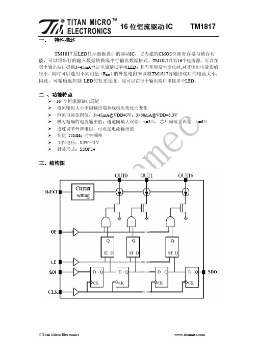
16 位恒流驱动 IC一、 特性描述TM1817TM1817是LED显示面板设计的驱动IC,它内建的CMOS位移寄存器与锁存功能,可以将串行的输入数据转换成平行输出数据格式。
TM1817具有16个电流源,可以在 每个输出端口提供3~45mA恒定电流量以驱动LED;且当环境发生变化时,对其输出电流影响 很小。
同时可以选用不同阻值(REXT)的外接电阻来调整TM1817各输出端口的电流大小, 因此,可精确地控制 LED的发光亮度。
也可以在每个输出端口串接多个LED。
二 、功能特点16 个恒流源输出通道 电流输出大小不因输出端负载电压变化而变化 恒流电流范围值,3~45mA@VDD=5V;3~30mA@VDD=3.3V 极为精确的电流输出值,通道间最大误差:<±3%,芯片间最大误差:<±6% 通过调节外部电阻,可设定电流输出值 高达 25MHz 时钟频率 工作电压:3.3V~5V 封装形式:SSOP24三、结构图©Titan Micro Electronics16 位恒流驱动 IC四、封装示意图TM1817SSOP24 五、管脚说明 名称 GND SDI CLK LE OUT0~OUT15 OE 控制逻辑及驱动电流的接地端 串行数据输入端 时钟信号的输入端,时钟上升时移位数据 数据锁存控制端。
当LE是高电平时,串行数据会被传入至输入锁存器; 当LE是低电平时,资料会被锁存 恒流源输出端 输出使能控制端,当 OE 是低电平时,即会启动 OUT0~OUT15 输出;当 OE 是高电平时,OUT0~OUT15 输出会被关闭 SDO R—EXT 串行数据输出端;可接至下一个芯片的 SDI 端口 连接外接电阻的输入端;此外接电阻可设定所有输出通道的 输出电流 VDD 芯片电源 功能说明©Titan Micro Electronics16 位恒流驱动 IC六、 输出及输入等效电路TM1817七、 时序图©Titan Micro Electronics16 位恒流驱动 IC八 、真值表TM1817九、最大限定范围特性 电源电压 输入端电压 输出端电流 输出端承受电压 代表符号 VDD 最大限定范围 0~6.0 -0.4~VDD+0.4V +65 -0.5~+6.0 单位 V V mA VVINIOUTVDS时钟频率 IC 工作时的环境温度 IC 储存时的环境温度FCLKTopr Tstg25 -40~+85 -55~+150MHZ.. ..©Titan Micro Electronics16 位恒流驱动 IC十、直流特性(VDD=5.0V)特性 电源电压 输出端承受电压 代表符号 VDD 测量条件 -----------OUT0~OUT15 参考直流特性的测试电路 ------------------Ta=-40~85℃ Ta=-40~85℃ 最小值 4.5 ----3 --------0.7* VDD GND --------4.6 ------------------------250 250 ----------------------------------15 ---30TM1817一般值 5.0 --------------------最大值 5.5 5 45 -8.2 8.2 VDD 0.3* VDD 0.5 0.4 --------±3℅ ----±3℅ ±0.1 ﹪ ±1﹪ 500 500 2.5 4.5 6 5.2 6.5 --------800 800 5.0 7.0 9.0 8.5 9.5 mA ℅/V ℅/V KΩ KΩ mA 单位 V V mA mA mA V V μA V V mAVDS IOUT IOH IOLSDO 输出端电流输出高 输出端电 压 电平 输出低 电平 输出端漏电流 输出端电压 输出端电流 1 输出电流误差 输出端电流 2 输出电流误差 输出电流误差/VDS 变 化量 输出端电流误差/VDD 变化量 Pull-up 电阻 Pull-down 电阻VIH VILVOH VOLVOHVDS=18 IOL=+1mAIOH=1mA VDS=1V Iol=26.25mA VDS=0.6V VDS=0.8V Iol=52.5mA VDS=0.8V VDS=1.0V~3.0V VDD=4.5V~5.5V 0E LE Rext=未接, OUT0~ OUT15=OFF Rext=1240Ω, OUT0~ OUT15=OFF Rext=620Ω, OUT0~ OUT15=OFF Rext=1240Ω, OUT0~ OUT15=ON Rext=620Ω, OUT0~ OUT15=ON Rext=620Ω Rext=620Ω Rext=1246Ω Rext=1246ΩIOUT1dIOUT2 IOUT2 dIOUT2﹪/△VDS ﹪/△VDDRIN(up) RIN(down)IDD(off)1IC 工作电流IDD(off)2 IDD(off)3 IDD(on)1 IDD(on)2注:Ta 为环境温度©Titan Micro Electronics16 位恒流驱动 IC十一、直流特性(VDD=3.3V)特性 电源电压 输出端承受电压 代表符号 VDD 测量条件 -----------OUT0~OUT15 参考直流特性的测试电路 ------------------Ta=-40~85℃ Ta=-40~85℃ 最小值 3.0 ----3 --------0.8VD D GND --------4.6 ------------------------26.25 ±1TM1817一般值 3.3 --------------------最大值 3.6 5 30 -8.2 8.2 VDD 0.3* VDD 0.5 0.4 --------±3℅ 单位 V V mA mA mA V V μA V V mAVDS IOUT IOH IOLSDO 输出端电流输出高 输出端电 压 电平 输出低 电平 输出断漏电流 输出端电压 输出端电流 1 输出电流误差VIH VILVOH VOL VOH IOUT1 dIOUT2VDS=18 IOL=+1mAIOH=-1mAVDS=1VIOL=26.25m A VDS=1.0V Rext=1860Ω Rext=1860Ω输出端电流 2 输出电流误差 输出电流误差/VDS 变化量 输出端电流误差 /VDD 变化量 Pull-up 电阻 Pull-up 电阻IOUT2 dIOUT2﹪/△VDS ﹪/△VDDVDS=1.0V Iol=30mA VDS=1.0VRext=744Ω Rext=744Ω----------------250 250 -------------------52.5 ±0.1 ℅ ±1℅ 500 500 500 1.8 4.1 5.2 4.5 5.4----±3℅ --------800 800 5.0 7.0 9.5 7.0 8.5mAVDS=1.0V~3.0V VDD=3.0V~3.6V OE LE Rext=未接, OUT0~ OUT15=OFF Rext=1860Ω, OUT0~ OUT15=OFF Rext=744Ω, OUT0~ OUT15=OFF Rext=1860Ω, OUT0~ OUT15=ON Rext=744Ω, OUT0~ OUT15=ON℅/V ℅/V KΩ KΩRIN(up) RIN(down)IDD(off)1IDD(off)2IC 工作电流IDD(off)3 IDD(off)1 IDD(off)2mA©Titan Micro Electronics16 位恒流驱动 IC十二、直流特性的测试电路TM1817十三、动态特性(VDD=5.0V)特性 CLK-OUT 延迟时间 (低电平到高电平) LE-OUT OE-OUT CLK-SDO CLK-OUT 延迟时间 (高电平到低电平) 电流输出上升时间 电流输出下降时间 LE-OUT OE-OUT CLK-SDO 代表符 tpLH1 tpLH2 tpLH3 tpLH tpLH1 tpLH2 tpLH3 tpLH tor tof 测量条件 最小值 ---一般值 80 80 115 20 80 80 115 20 160 70 最大值 100 100 135 40 100 100 135 40 180 90 单位 ns ns n ns ns ns ns ns ns nsVDD=5.0V VDS=1.0V VIH=VddVIL=GND Rext=830Ω----------------------------VL=4.5V RL=100Ω CL=10pF十四、动态特性(VDD=3.3V)特性 CLK-OUT 延迟时间©Titan Micro Electronics代表符测量条件最小值 ----一般值 80 80最大值 100 100单位 ns nstpLH1tpLH2LE-OUTVDD=3.3V----16 位恒流驱动 IC(低电平到高电平) OE-OUT CLK-SDO CLK-OUT 延迟时间 (高电平到低电平) LE-OUT OE-OUT CLK-SDO 电流输出上升沿时间 电流输出下降沿时间TM1817115 20 80 80 115 20 160 70 135 40 100 100 135 40 180 90 n ns ns ns ns ns ns nstpLH3 tpLH tpLH1 tpLH2 tpLH3 tpLH tor tofVDS=1.0V VIH=VddVIL=GND Rext=830Ω VL=3V RL=100Ω CL=10pF-------------------------十五、动态特性的测试电路十六、时序波形图©Titan Micro Electronics16 位恒流驱动 ICTM1817十七、应用信息将 TM1817 应用与 LED 面板设计上时,通道间甚至芯片间的电流差异极小。
tm070rdh12_f_v2.0
MODEL NO. : TM070RDH12ISSUED DATE: 2010-08-26VERSION : Ver 2.0□Preliminary Specification■Final Product SpecificationCustomer :Approved by NotesSHANGHAI TIANMA Confirmed :Prepared by Checked by Approved byThis technical specification is subjected to change without noticeThe information contained herein is the exclusive property of SHANGHAI TIANMA MICRO-ELECTRONICS Corporation, and shall not be distributed, reproduced, or disclosed in whole or in part without prior writtenTable of ContentsTable of Contents (2)Record of Revision (3)1General Specifications (4)2Input/Output Terminals (5)3Absolute Maximum Ratings (7)4Electrical Characteristics (8)5Timing Chart (13)6Optical Characteristics (17)7Environmental / Reliability Test (20)8Mechanical Drawing (21)9Packing Drawing (22)10Precautions for Use of LCD Modules (24)The information contained herein is the exclusive property of SHANGHAI TIANMA MICRO-ELECTRONICS Corporation, and shall not be distributed, reproduced, or disclosed in whole or in part without prior writtenRecord of RevisionRev Issued Date Description Editor1.0 2010-06-07 Preliminary Specification Release Xing Nie2.0 2010-0-26 Final Product Specification Release Xing NieThe information contained herein is the exclusive property of SHANGHAI TIANMA MICRO-ELECTRONICS Corporation, and shall not be distributed, reproduced, or disclosed in whole or in part without prior writtenThe information contained herein is the exclusive property of SHANGHAI TIANMA MICRO-ELECTRONICS Corporation, and shall not be distributed, reproduced, or disclosed in whole or in part without prior written1 General SpecificationsFeatureSpecSize 7.0 inch Resolution 800(RGB) x 480Interface RGB 24 bit with TCON Color Depth 16.7MTechnology Typea-SiPixel Pitch (mm) 0.1926x0.1790Pixel Configuration R.G.B. Vertical Stripe Display ModeTM with Normally White Surface Treatment(Up Polarizer) Anti Glare Viewing Direction12 o’clock Display Spec.Gray Scale Inversion Direction 6 o’clock LCM (W x H x D) (mm) 164.9x100.0x5.7 Active Area(mm)154.08X85.92 With /Without TSP Without TSP Weight (g) TBD Mechanical CharacteristicsLED Numbers21 LEDsNote 1: Viewing direction for best image quality is different from TFT definition. There is a 180degree shift.Note 2: Requirements on Environmental Protection: Q/S0002 Note 3: LCM weight tolerance: +/- 5%2 Input/Output Terminals2.1 CN1 of FPCMatching Connector: FH28-60S-0.5SHPin No Symbol I/O DescriptionRemark1 AGND P Ground2 AVDD P Analog power3 VCC P Digital power supply4 R0 I Red data(LSB)5 R1 I Red data6 R2 I Red data7 R3 I Red data8 R4 I Red data9 R5 I Red data 10 R6 I Red data 11 R7 I Red data(MSB) 12 G0 I Green data(LSB) 13 G1 I Green data 14 G2 I Green data 15 G3 I Green data 16 G4 I Green data 17 G5 I Green data 18 G6 I Green data 19 G7 I Green data(MSB)20 B0 I Blue data(LSB) 21 B1 I Blue data 22 B2 I Blue data 23 B3 I Blue data 24 B4 I Blue data 25 B5 I Blue data 26 B6 I Blue data 27 B7 I Blue data(MSB) 28 DCLK I Clock input 29 DE I Data enable signal. Active high to enable data 30 HSD I Horizontal sync input. negative polarity 31 VSD I Vertical sync input. negative polarity32 MODE I DE/SYNC mode select.H: DE mode ,L: SYNC mode 33 RSTB I Global reset pin34 STBYB I Standby mode selectH: normal operation, L: standby mode 35 SHLR I Source right or left sequence control36 VCC P Digital power 37 UPDN I Gate up or down scan control38 GND P Ground 39 AGND P Ground 40 AVDD P Analog power 41 VCOM I Common voltage inputThe information contained herein is the exclusive property of SHANGHAI TIANMA MICRO-ELECTRONICS Corporation, and shall not be distributed, reproduced, or disclosed in whole or in part without prior writtenThe information contained herein is the exclusive property of SHANGHAI TIANMA MICRO-ELECTRONICSCorporation, and shall not be distributed, reproduced, or disclosed in whole or in part without prior written 42 DITH I Dithering setting.H: 6bit resolution, L: 8bit resolution 43 NC - Not connect 44 NC - Not connect 45 V10 I Gamma voltage 10 46 V9 I Gamma voltage 9 47 V8 I Gamma voltage 8 48 V7 I Gamma voltage 7 49 V6 I Gamma voltage 6 50 V5 I Gamma voltage 5 51 V4 I Gamma voltage 4 52 V3 I Gamma voltage 3 53 V2 I Gamma voltage 2 54 V1 I Gamma voltage 1 55 NC - Not connect 56 VGH P Positive power for TFT 57 VCC P Digital power 58 VGL P Negative power for TFT 59 GND P Ground 60 NC - Not connectNote: I/O definition.I---Input pin, O---Outputpin, P--- Power/Ground, N--- No Connection2.2 CN2 of LED BLU ConnectorPin Symbol I/O Description Remark 1 LED+ P LED Anode Red Cable 2LED-PLED CathodeWhite Cable2.3 U/D R/L Function DescriptionScan Control InputUPDN SHLR Scanning Direction GND VCC Up to Down, Left to Right VCC GND Down to Up, Right to Left GND GND Up to Down, Right to Left VCCVCCDown to Up, Left to RightThe information contained herein is the exclusive property of SHANGHAI TIANMA MICRO-ELECTRONICSCorporation, and shall not be distributed, reproduced, or disclosed in whole or in part without prior written3 Absolute Maximum RatingsAGND= GND=0V, Ta = 25 ℃ItemSymbolMinMaxUnitRemarkVCC -0.50 5.00 V AVDD -0.50 15.00 VVGH -0.30 42.00 V VGL -20.00 0.30 V Power VoltageVGH-VGL-0.30 40.00 V Backlight Forward Current I LED -25.0mAFor each LEDOperating Temperature T OPR -20.0 70.0 ℃ Storage Temperature T STG-30.080.0℃The information contained herein is the exclusive property of SHANGHAI TIANMA MICRO-ELECTRONICSCorporation, and shall not be distributed, reproduced, or disclosed in whole or in part without prior written4 Electrical Characteristics4.1Recommended Operating ConditionAGND=GND=0V, Ta = 25℃ParameterSymbolMIN TYP MAX Unit Remark Digital supply Voltage VCC 3.00 3.30 3.60 V Analog supply Voltage AVDD 10.07 10.6011.13 V Gate on voltage VGH 14.40 16.0017.60 V Gate off voltage VGL-7.70-7-6.30 VCommon Electrode Driving SignalVCOM -4.30- VV1~V5 0.4*AVDD - AVDD-0.4V Input level of Gamma voltage V6~V10 0.1 - 0.6*AVDD VLow Level V IL 0 - 0.3*VCC VInput Signal VoltageHigh LevelV IH 0.7*VCC - VCC V R0~R7,G0~G7,0~B7,DE, DCLK,HSD,VSD,MODE, RSTB,STBYB,SHLR,UPDN, DITHCurrent of digital supply voltageI VCC - - 10 mAVCC=3.3V color bar patternCurrent of analog supply voltageI AVDD - - 40 mAAVDD=Typ color bar patternCurrent of Gate on voltage I VGH - - 0.3 mA VGH=22.0V Current of Gate off voltageI VGL- - 0.3 mA VGL =-7.0VNote: The value is for design stage only.4.2 Gamma Correction Reference Voltage SettingGamma Correction CurveGamma Correction Reference Voltage SettingParameterSymbolMINTYPMAXUnit RemarkV1 - 10.14 AVDD-0.4 VV2 - 8.25 - V V3 - 7.66 - V V4 - 7.19 - V V5 - 5.10 - V V6 - 5.50 - V V7 - 3.41 - V V8 - 2.94 - V V9 - 2.35 - V Gamma correctionreference voltageV1~V10V10 AGND+0.10.46- VNote: the value is for design stage only;AVDD-0.4> V1 > V2> V3 > V4 > V6 > V5 > V7>V8 > V9 > V10 > AGND+0.1VGamma Correction Reference CircuitThe information contained herein is the exclusive property of SHANGHAI TIANMA MICRO-ELECTRONICSCorporation, and shall not be distributed, reproduced, or disclosed in whole or in part without prior writtenGamma Correction Resistance ValueSymbol Unit Resistance Symbol Unit Resistance R1// R2 Ω 47//NC R3// R4 Ω 240//620R5// R6 Ω 240//1000R7// R8 Ω 62//220R9// R10 Ω 91//180R11// R12 Ω 91//180R13// R14 Ω 62//220R15// R16 Ω 240//1000R17// R18 Ω 240//620R19// R20 Ω 47//NCR21// R22 Ω 47//300C1~C10 uF 1.0(16V)Note: Setting the resistance only when AVDD=10.60V, AGND=GND=0VThe information contained herein is the exclusive property of SHANGHAI TIANMA MICRO-ELECTRONICS Corporation, and shall not be distributed, reproduced, or disclosed in whole or in part without prior written4.3Recommended Driving Condition for BacklightTa=25℃ ItemSymbol MinTypMaxUnitRemarkForward Current I F - 140.0- mAForward VoltageV F - 9.6 11.4 V Backlight Power ConsumptionW BL- 1344 - W 21LEDs(3 LED Serial, 7 LED Parallel)Note 1: The LED driving condition is defined for total backlight consumption, and which depend on Forward Current setting.Note 2: Forward Voltage is just for reference for one serial.The information contained herein is the exclusive property of SHANGHAI TIANMA MICRO-ELECTRONICS Corporation, and shall not be distributed, reproduced, or disclosed in whole or in part without prior writtenDiagram4.4 Block Array The information contained herein is the exclusive property of SHANGHAI TIANMA MICRO-ELECTRONICSCorporation, and shall not be distributed, reproduced, or disclosed in whole or in part without prior writtenThe information contained herein is the exclusive property of SHANGHAI TIANMA MICRO-ELECTRONICS Corporation, and shall not be distributed, reproduced, or disclosed in whole or in part without prior written5 Timing Chart5.1TFT-LCD Input TimingVCC=3.3V, AGND=GND=0V, Ta=25℃ParameterSymbolMinTypMaxUnitRemarkFclk -30 40MHZDCLKtclk - 33.3 25.0 ns th 928 928 928 tclk thd 800 800 800 tclkthpw 1 48 - tclk thb 88 88 88 tclk HSDthfp 1 40 - tclk tv 513 525 - th tvd 480 480 480 thtvpw 3 3 - th tvb 32 32 32 thVSDtvfp 1 13 - thNote: DE timing refer to HSD, VSD input timing. TCON Horizontal Input Timing DiagramTCON Vertical Input Timing Diagram HV5.2 Input timing Characteristics of Interface(DCLK,VSD,HSD,DE)(VCC=3.3V, AVSS=GND=0V, Ta=25℃) Parameter Symbol Min Typ Max Unit RemarkDCLK frequency Fclk - 30.040.0MHzThe information contained herein is the exclusive property of SHANGHAI TIANMA MICRO-ELECTRONICS Corporation, and shall not be distributed, reproduced, or disclosed in whole or in part without prior writtenDCLK cycle time Tcph - 33.325 nsDCLK pulse width Tcw 40%50%60%TcphVSD setup time Tvst 8 nsVSD hold time Tvhd 8 - - nsHSD setup time Thst 8 nsHSD hold time Thhd 8 - - nsData setup time Tdsu 8 ns Data to DCLKData hold time Tdhd 8 - - ns Data to DCLKDE setup time Tesu 8 - - nsDE hold time Tehd 8 - - ns5.3 Enter and Exit Standby Mode SequenceThe information contained herein is the exclusive property of SHANGHAI TIANMA MICRO-ELECTRONICS Corporation, and shall not be distributed, reproduced, or disclosed in whole or in part without prior written6. POWER ON/OFF SEQUENCENote: T1≥20ms, T2≥20ms, T3≥5ms, T4≥100ms, T5≥5ms, T6≥5ms.The information contained herein is the exclusive property of SHANGHAI TIANMA MICRO-ELECTRONICS Corporation, and shall not be distributed, reproduced, or disclosed in whole or in part without prior writtenThe information contained herein is the exclusive property of SHANGHAI TIANMA MICRO-ELECTRONICS Corporation, and shall not be distributed, reproduced, or disclosed in whole or in part without prior written6 Optical CharacteristicsTa=25℃ItemSymbol ConditionMinTypMaxUnitRemarkθT 50 60 --θB 60 70 --θL 60 70 -- View AnglesθRCR ≧10 60 70 -- Degree Note 2Contrast Ratio CR θ=0°400 500 --Note1Note3T ON Response TimeT OFF 25℃ -- 20 30 msNote1Note4x 0.274 0.324 0.374 White y 0.295 0.345 0.395 x 0.544 0.594 0.644Redy 0.301 0.351 0.401x 0.299 0.349 0.399Green y 0.531 0.581 0.631 x 0.102 0.152 0.202 ChromaticityBlueyBacklight is on 0.053 0.103 0.153Note1Note5Uniformity U 75 80 -- %Note1Note6NTSC -- 50 -- % Note 5 Luminance L 280 350 -- cd/m 2Note1 Note7 Test Conditions:1. I F = 160 mA, V F =9.6V, and the ambient temperature is 25. ℃2. The test systems refer to Note 1 and Note 2.Note 1: Definition of optical measurement system.The optical characteristics should be measured in dark room. After 5 Minutes operation, the optical properties are measured at the center point of the LCD screen. All input terminals LCD panel must be ground when measuring the center area of the panel.The information contained herein is the exclusive property of SHANGHAI TIANMA MICRO-ELECTRONICS Corporation, and shall not be distributed, reproduced, or disclosed in whole or in part without prior written“White state “: The state is that the LCD should drive by Vwhite. “Black state”: The state is that the LCD should drive by Vblack. Vwhite: To be determined Vblack: To be determined. Note 4: Definition of Response timeThe response time is defined as the LCD optical switching time interval between “White” state and“Black” state. Rise time (T ON) is the time between photo detector output intensity changed from 90% to 10%. And fall time (T OFF) is the time between photo detector output intensity changed from 10% to 90%.Note 5: Definition of color chromaticity (CIE1931)Color coordinates measured at center point of LCD.Note 6: Definition of Luminance UniformityActive area is divided into 9 measuring areas (Refer Fig. 2). Every measuring point is placed at the center of each measuring area.Luminance Uniformity (U) = Lmin/ LmaxL-------Active area length W----- Active area widthLmax: The measured Maximum luminance of all measurement position.Lmin: The measured Minimum luminance of all measurement position.Note 7: Definition of Luminance:Measure the luminance of white state at center point.The information contained herein is the exclusive property of SHANGHAI TIANMA MICRO-ELECTRONICS Corporation, and shall not be distributed, reproduced, or disclosed in whole or in part without prior writtenThe information contained herein is the exclusive property of SHANGHAI TIANMA MICRO-ELECTRONICSCorporation, and shall not be distributed, reproduced, or disclosed in whole or in part without prior written7 Environmental / Reliability TestNo Test Item ConditionRemarks1 High Temperature OperationTs = +70, 240 hours ℃ IEC60068-2-1 GB2423.2 2 Low Temperature OperationTa = -20, 240 hours ℃ IEC60068-2-1 GB2423.1 3 High Temperature StorageTa = +80℃, 240 hours IEC60068-2-1 GB2423.2 4 Low Temperature StorageTa = -30℃, 240 hoursIEC60068-2-1 GB2423.1 5Storage at High Temperature and HumidityTa = +60℃, 90% RH max,240hoursIEC60068-2-78 GB/T2423.36Thermal Shock (non-operation) -30℃ 30 min~+80℃ 30 min, Change time:5min, 100 Cycle Start with cold temperature,End with high temperature,IEC60068-2-14 GB2423.227 ESDC=150pF,R=330Ω,5point/panel Air:±8Kv,5times;Contact:±4Kv,5times (Environment:15℃~35℃, 30%~60%.86Kpa~106Kpa) IEC61000-4-2GB/T17626.28 Vibration Test Frequency range:10~55Hz Stroke:1.5mmSweep:10Hz~55Hz~10Hz2 hours for each direction of X.Y .Z. (6 hours for total)IEC60068-2-6GB/T2423.109 Mechanical Shock (Non Op)Half Sine Wave100G 6ms, ±X,±Y ,±Z3times for each direction IEC60068-2-27 GB/T2423.5 10 Package Drop TestHeight:60cm, 1corner,3edges,6surfaces IEC60068-2-34GB/T2423.11 Note1: Ts is the temperature of panel’s surface. Note2: Ta is the ambient temperature of samples.The information contained herein is the exclusive property of SHANGHAI TIANMA MICRO-ELECTRONICS Corporation, and shall not be distributed, reproduced, or disclosed in whole or in part without prior writtenThe information contained herein is the exclusive property of SHANGHAI TIANMA MICRO-ELECTRONICSCorporation, and shall not be distributed, reproduced, or disclosed in whole or in part without prior written NoItemModel(Material)Dimensions(mm)Unit Weigt (Kg) Quantity Remark 1 LCM module TM070RDH12164.90*100.00*5.70TBD 50 2 Partition_1 Corrugated Paper 513*333*215 2.013. Anti-StaticBag PE 160*178*0.05 0.01 50 Anti-static4 Dust-ProofBagPE 700*545 0.0600 15 Partition_2 Corrugated Paper 505*332 0.1 26 Corrugated Bar Corrugated Paper513*148 0.06 4 7 Beauty-grain Tape 30*10 TBD 150 8 Dessicant Dessicant 45*350.002 8 9 Carton Corrugated Paper 530*350*2501.1000110 Total weight TBD ±5%The information contained herein is the exclusive property of SHANGHAI TIANMA MICRO-ELECTRONICS Corporation, and shall not be distributed, reproduced, or disclosed in whole or in part without prior writtenSHANGHAI TIANMA MICRO-ELECTRONICS TM070RDH12 V2.0The information contained herein is the exclusive property of SHANGHAI TIANMA MICRO-ELECTRONICS Corporation, and shall not be distributed, reproduced, or disclosed in whole or in part without prior written10 Precautions for Use of LCD Modules10.1 Handling Precautions10.1.1 The display panel is made of glass. Do not subject it to a mechanical shock by dropping it from a high place, etc.10.1.2 If the display panel is damaged and the liquid crystal substance inside it leaks out, be sure not to get any in your mouth, if the substance comes into contact with your skin or clothes, promptly wash it off using soap and water.10.1.3 Do not apply excessive force to the display surface or the adjoining areas since this may cause the color tone to vary.10.1.4 The polarizer covering the display surface of the LCD module is soft and easily scratched. Handle this polarizer carefully.10.1.5 If the display surface is contaMinated, breathe on the surface and gently wipe it with a soft dry cloth. If still not completely clear, moisten cloth with one of the following solvents: - Isopropyl alcohol - Ethyl alcoholSolvents other than those mentioned above may damage the polarizer. Especially, do not use the following: - Water - Ketone- Aromatic solvents10.1.6 Do not attempt to disassemble the LCD Module.10.1.7 If the logic circuit power is off, do not apply the input signals.10.1.8 To prevent destruction of the elements by static electricity, be careful to maintain an optimum work environment.10.1.8.1 Be sure to ground the body when handling the LCD Modules.10.1.8.2 Tools required for assembly, such as soldering irons, must be properly ground. 10.1.8.3 To reduce the amount of static electricity generated, do not conduct assembly and other work under dry conditions.10.1.8.4 The LCD Module is coated with a film to protect the display surface. Be care when peeling off this protective film since static electricity may be generated. 10.2 Storage precautions10.2.1 When storing the LCD modules, avoid exposure to direct sunlight or to the light of fluorescent lamps.10.2.2 The LCD modules should be stored under the storage temperature range. If the LCD modules will be stored for a long time, the recommend condition is: Temperature : 0 ℃~ 40 Relatively humidity: ≤80%℃10.2.3The LCD modules should be stored in the room without acid, alkali and harmful gas.10.3 Transportation Precautions10.3.1 The LCD modules should be no falling and violent shocking during transportation, and also should avoid excessive press, water, damp and sunshine.。
三星AMOLED驱动芯片中文版说明书
表 5 所示为其他端口。 Symbol I/O 功能描述 DUMMYR[3:1] 电阻测量管脚,正常情况下悬空。 DUMMYL[3:1] DUMMY 无用管脚,悬空即可。 V0/V63 O 伽玛电压镜像管脚。 VDD3DUM O 内部与 VDD3 接在一起。
VSSDUM FUSE_EN RTEST EN_EXCLK EN_CLK TEST_MODE[1:0] TEST_IN[6:0] TE TEST_OUT[2:0]
表 2 系统接口
表3为 Symbol MDP MDN MSP MSN GPIO[9:0] (DB[17:8]) S_CSB(DB [7])
MDDI 管脚作用。 I/O 功能描述 I/O MDDI 数据输入/输出正端,如果 MDDI 不用,该端口悬空。 I/O MDDI 数据输入/输出负端,如果 MDDI 不用,该端口悬空。 I MDDI 数据选通输入正端,如果 MDDI 不用,该端口悬空。 I MDDI 数据选通输入负端,如果 MDDI 不用,该端口悬空。 I/O 总体输入输出,如果在 MDDI 中没有用 GPIO 的话,这些管 脚应该置地。 O 子屏幕驱动 IC 片选信号。 低电平时说明子屏幕驱动 IC 可用,高电平时说明子屏幕驱动
表 1 电源接口
如表 2 所示为系统接口。 Symbol I/O 功能描述 S_PB I 选择 CPU 接口模式,低电平时为并行接口,高电平时为串行 接口。 MDDI_E I 选择 MDDI 接口,低电平时 MDDI 接口不可用,高电平时 N MDDI 接口可用。 ID_MIB I 选择 CPU 种类, 低电平为 intel 80 系列 CPU, 高电平为 motorola 68 系列 CPU,如果 S_PB 是高电平,该端口为 ID 设置端口。 CSB I 片选信号,低电平芯片可用,高电平芯片不可用。 RS I 寄存器选择管脚。 低电平时,指令/状态,高电平时为指令参数/RAM 数据。 不用时需与 VDD3 接在一起。 RW_WR I 管脚作用 CPU 种类 管脚说明 B/SCL RW 68 系列 读写选择,低电平写,高电平读。 WRB 80 系列 写选通作用,在上升沿捕获数据。 SCL 串行接口 时钟同步信号。 E_RDB I 管脚作用 CPU 种类 管脚说明 E 68 系列 读写操作使能端。 RDB 80 系列 读选通作用,低电平时读出数据。 选择串行模式时,将此端口接在 VDD3 上。 SDI I 串行接口的数据输入接口,在 SCL 上升沿捕捉到输入数据,
天微产品选型表

固定花样三色灯驱动IC 6路LED恒流驱动IC LED照明及装饰驱动IC 9路LED恒流驱动IC LED照明及装饰驱动IC LED照明及装饰驱动IC LED照明及装饰驱动IC LED照明及装饰驱动IC LED照明及装饰驱动IC LED照明及装饰驱动IC LED照明及装饰驱动IC LED照明及装饰驱动IC
产品型号 TC1011 TC1006 TC1005 TC1003 TM1108 TM1107 TM1106 TM1105 TM1102 TM1103 TM1101 TM-SX670 TC1002
产品类型 电机控制专用IC 电机控制专用IC 电机控制专用IC 电机控制专用IC 仪器仪表专用IC 仪器仪表专用IC 仪器仪表专用IC 仪器仪表专用IC 仪器仪表专用IC 仪器仪表专用IC 仪器仪表专用IC 系统控制专用IC 电机控制专用IC
电力电子专用控制IC 电源管理IC
场效应管(MOSFET)
M1N60A M1N60B M1N60C M1N65 M1N65A M1N65B M2N60 M2N60B M2N65 M3N60 M3N65 M4N60 M4N65 M5N60 M5N65 M6N65 M7N65 M8N60 M8N65 M9N60
产品型号 TM1621 721 TM1722 TM1723 TM1726 TM1727 TM1728 TM1729 TM1730 TM75823
产品类型 LCD面板显示驱动IC LCD面板显示驱动IC LCD面板显示驱动IC LCD面板显示驱动IC LCD面板显示驱动IC LCD面板显示驱动IC LCD面板显示驱动IC LCD面板显示驱动IC LCD面板显示驱动IC LCD面板显示驱动IC
LED照明及装饰驱动IC
特性描述 1路恒流驱动,15~45mA电流,端口耐压24V 输入电压1.5V,升压驱动,80~200mA电流 3路恒流驱动,单线级联,灰度256级可调 3路恒流驱动,单线级联,灰度2568级可调,工作电压6~24V
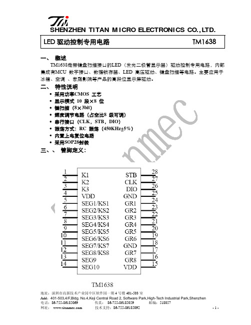
TM1638规格书
Add:401-503,4/F,Bldg. No.4,Keji Central Road 2, Software Park,High-Tech Industrial Park,Shenzhen
电话:86-755-86185069
传真: 86-755-86185059
邮编:518057
网址:
℃
储存温度
Tstg
-65 ~+150
℃
正常工作范围(Ta = -20 ~ +70℃,Vss = 0 V)
参数
符号
最小
典型 最大 单位
逻辑电源电压
VDD
5
V
高电平输入电压
VIH
0.7 VDD
-
VDD
V
测试条件 -
低电平输入电压
VIL
0
-
0.3 VDD
V
-
电气特性(Ta = -20 ~ +70℃,VDD = 4.5 ~ 5.5 V, Vss = 0 V
技术支持:86-755-86185092
-1-
深圳市天微电子有限公司
SHENZHEN TITAN M ICRO ELECTRONI CS CO.,LTD.
四、管脚功能说明:
符号
管脚名称
说明
DIN
数据输入
在时钟上升沿输入串行数据,从低位开始
DOUT STB
数据输出
在时钟下降沿输出串行数据,从低位开始。输出 为N-ch open drain
二、 特性说明
• 采用功率CMOS 工艺 • 显示模式 10 段×8 位 • 键扫描(8×3bit) • 辉度调节电路(占空比8 级可调) • 串行接口(CLK,STB,DIO) • 振荡方式:RC 振荡(450KHz+5%) • 内置上电复位电路 • 采用SOP28封装
TM系列集成电路产品手册第二版
TM 系列集成电路产 品 手 册(第二版)深圳市天微电子有限公司Shenzhen Titan Micro Electronics Co., Ltd.http://www.titanmec.om/前言天微产品涵盖电源管理产品线、检测与计量产品线、照明及显示驱动产品线等系列产品,产品众多,每个产品都有详细的产品规格书。
随着公司的蓬勃发展,产品越来越多。
编写本手册目的是把公司自2003年以来的所有产品进行归类,便于公司各部门以及客户全面地系统地了解天微的芯片。
由于产品规格书不是同一个人,也不是同一时期编写的,里面的引脚图,采用了不同的格式,特别的图片格式的,放大或缩小容易失真,打印不清晰。
在这里,编者用AutoCAD 2010重画了所有的芯片引脚图,这样的图是矢量图,任意放大或缩小不会失真,双击图形可直接进入AutoCAD 中进行修改。
建议大家用AutoCAD 2010绘图软件。
本手册的产品分类是根据服务器上的规格书重新分类的。
相比较2012年8月30日编写的《TM 系列集成电路产品手册》第一版,分类方法略有不同,。
目前的集成电路主要包括:1. LCD驱动2. LED看板驱动3. LED面板驱动4. LED照明及装饰驱动5. 通用器件6. 电机驱动7. 电能计量8. 红外控制9. 音频及视频处理10.模数转换器11.数模转换器12.电源管理13.其它。
在产品简介中注明了产品的型号、封装形式、名称、主要特点、应用领域、引脚图、典型应用电路图等。
本手册中没有录入某些很老的产品或还未正式规格书的新产品。
本手册未录入的产品有:TM74HC74,TM7758,TM7760,TM7762、TA1669、TA1672、TA1673、TM1670、TM1623C、TM1669、TA9909、TA9909B、TA9912、TA9912B、TM1933、TM1836、TM1904、TM1909、TM1912、TM1913、TM1925、TM2101、TM2104、TM2202、TM9105等等。
- 1、下载文档前请自行甄别文档内容的完整性,平台不提供额外的编辑、内容补充、找答案等附加服务。
- 2、"仅部分预览"的文档,不可在线预览部分如存在完整性等问题,可反馈申请退款(可完整预览的文档不适用该条件!)。
- 3、如文档侵犯您的权益,请联系客服反馈,我们会尽快为您处理(人工客服工作时间:9:00-18:30)。
--
最小值 -
2.5 0.6 1.3 100 100 1.3 0.6 0.6 0.6
TM1729 典型值
-
最大值 0.3 0.3 -
单位
us us us us us ns ns us us us us
8.4. 二线串行数据传输时间波形
SDA
t BUF
t LW
SCL
SDA
t HD:STA
tr
t SDH
SDA SCL
开始条件
停止条件
在利用2线I/F输入命令以及数据时必须形成开始条件和停止条件的固有形态发生。
Slave_Address S0 1111100AC
COMMAND
A C DISPLAY DATA A P
开始条件
ACK 命令或数据判定位
停止条件
本芯片在输入命令或显示数据时,必须按照以下步骤:
©Titan Micro Electronics
V1.0
2
6. 输入/输出等效电路
VDD
VDD
VLCD
GND
GND
52 SEG×4 COM LCD 驱动芯片 TM1729
VDD TEST1
GND
VDD TEST2
GND
SDA
SCL
VDD
OSCIO
GND
GND
GND
2. 功能特点
工作电压范围:2.5~5.5V 液晶驱动输出:52 SEG×4 COM 内置DDRAM显存容量:52×4=208bit 液晶驱动模式:1/3Bias、1/2Bias 液晶翻转模式:Line、Frame 串行数据输入接口:SCL、SDA 低功耗设计 内置振荡电路 搭载等待模式 内置上电复位功能 搭载闪烁模式 封装形式: TSSOP48,SSOP48,LQFP64
命令的MSB位是判断下一组数据是命令还是显示数据(即MSB位是Command或Display Data的判定位)。 Command或Display Data的判定位只有为“1”,才有可能输入后续的命令; Command或Display Data的判定位只有为“0”,才有可能输入后续的显示数据。
S
Slave_Address
1. 特性描述
52 SEG×4 COM LCD 驱动芯片 TM1729
TM1729 是一种低功耗的字段式LCD显示驱动控制专用芯片。它拥有52个SEG输出端、4个COM输 出端,内置52×4=208bit的DDRAM存,采用2线(SCL、SDA)串行传输数据,可以设置1/3Bias和1/2Bias 驱动模式,Line和Frame翻转模式。可广泛应用在电能表、功率计等仪器仪表上。本产品性能优良,质 量可靠。
I
2线串行时钟输入
SDA
16
20
I /O
2线串行数据输入
COM0~COM3
6~9
10~13
O
液晶驱动COMMON输出
26~37
SEG0~ SEG35
18~48 1~5
42~53 58~64
O
液晶驱动SEGMENT输出
1~6
7~9
SEG36~ SEG51
---
22~25 38~41
O
液晶驱动SEGMENT输出
3. 内部结构框图
COM0 COM3
SEG0 SEG51
VDD
COM驱动
VLCD OSCIO
GND
+ + -
LCD电压生成器
振荡器
LCD Bias 选择器
COM 计数器
闪烁 定时器
SEG驱动
DDRAM 显存
上电复位
命令寄存器
译码器
串行接口 IF 滤波器
SDA
SCL
©Titan Micro Electronics
54~57
*备注:上表中的管脚序号,不同的封装,脚位有所不一样,详情请参考管脚排列图。
集成电路系静电敏感器件,在干燥季节或者干燥环境使用容易产生大量静电,静电放电可
能会损坏集成电路,天微电子建议采取一切适当的集成电路预防处理措施,不正当的操作
焊接,可能会造成 ESD 损坏或者性能下降,芯片无法正常工作。
(1) 为了使POR电路工作而需满足tR,tF,tOFF,Vbot的推荐条件
tF
tR
推荐条件
tOFF
Vbot
tR
tF
tOFF
Vbot
1ms 1ms 100ms <0.1V
注意:在POR电路有效时,TEST2引脚必须置“L”。 (2) 在无法满足以上条件时,电源上升后请采取以下对策 注意:TEST2置高时,为了让POR电路变为有效必须采取以下对策: A. 停止条件为了在SCL-H的状态下,SDA由L变为H
(1)形成开始条件
(2)发送Slave Address
(3)命令,显示数据的传送
(4)形成停止条件
9.2. ACK信号
进行数据传输时,必须有ACK信号。传送的数据是由8bit为单位组成的,8bit数据传送传送后返回
ACK信号。
8bit数据(Slave Address,Command,Display Data)传送后,在SCL(第8个)信号下降时SDA数据线,
最小值 0.7VDD
GND -1 0 -
-
TM1729 典型值
3 3 -
7.5
最大值 VDD
0.3VDD 1 -
VDD-2.4 5
20
单位
V V uA uA kΩ kΩ V uA
uA
8.2. 振荡特性
在-45℃~+85℃下测试,VDD=2.5V~5.5V,除非另有说明
参数名称
参数符号
测试条件
内部振荡频率
输出“L”信号。然后第9个信号下降时输出停止。
但是,输出时为了NMOS开路的形式,H电平不输出。
在不需要ACK信号时,从SCL信号的第8个信号下降到第9个信号的下降为止请输入“L”。
开始条件
停止条件
SDA
SCL
1-7 8 9
1-7 8 9
1-7 8 9
ACK
ACKACKFra bibliotek9.3. Command的传送方法 开始条件生成后,输入Slave Address(0111 1100)。输入Slave Address后,必须输入1byte的命令。
最大值 5.5
VDD-2.4 +85 +125
单位
V V ℃ ℃
8. 芯片参数
8.1. 电气特性)
在-45℃~+85℃下测试,VDD=2.5V~5.5V,除非另有说明
参数名称
参数符号
测试条件
高电平输入电压
VIH
--
低电平输入电压
VIL
--
高电平输入电流
IIH
--
低电平输入电流
IIL
--
SEG液晶驱动电阻
COM0 COM1 COM2 COM3 VLCD
VDD GND TEST1 OSCIO SCL SDA TEST2 SEG0 SEG1 SEG2 SEG3 SEG4 SEG5 SEG6
1
48
2
47
3
46
4
45
5
44
6
43
7
42
8
41
9
40
10
39
11
38
12
37
13 TOP VIEW 36
14
TSSOP48 SSOP48
参数名称
参数符号
测试条件
输入信号上升时间
tr
--
输入信号下降时间
tf
--
SCL周期
tCYC
--
高电平SCL幅宽
tHW
--
低电平SCL幅宽
tLW
--
SDA 建立时间
tSDS
--
SDA 保持时间
tSDH
--
总线无效时间
tBUF
--
开始条件保持时间 tHD:STA
--
开始条件建立时间 tSU:STA
--
停止条件建立时间 tSU:STO
A1
Command
A0
Command
A
Display Data
A
P
在输入显示数据的状态时,就不能进行命令的输入。如果想再次输入命令的话,需要再次生成开始
条件。在命令传送的过程中,输入开始条件或停止条件时传送的命令就会被取消的,传送过程中输入开
始条件,下一个Slave Address输入后转换为命令输入状态。
7. 工作条件
7.1. 极限工作条件
参数名称
参数符号
极限值
单位
电源电压1
VDD
-0.5~+7.0
V
电源电压2
VLCD
-0.5~VDD
V
允许损耗
Pd
0.64
W
输入电压范围
VIN
-0.5~VDD+0.5
V
工作温度范围
Topr
-40~+85
℃
保存温度范围
tstg
-55~+125
℃
(1)芯片长时间工作在上述极限参数条件下,可能造成器件可靠性降低或永久性损坏,天微电子不建
45
SEG15
44
SEG14
43
SEG13
42
SEG12
41
SEG47
40
SEG46
39
SEG45
38
SEG44
37
SEG11
36
SEG10