带隙基准源电路与版图设计
无运放带隙基准电路设计
无运放带隙基准电路设计
运放带隙基准电路(opamp bandgap reference circuit)是一种基于运放的电路,用于提供稳定的参考电压。
它的设计基于运放的放大特性和电压反馈机制,通过差分放大和反馈调整,产生一个相对稳定的参考电压。
下面是一种常见的运放带隙基准电路的设计:
1. 选择一个适当的运放芯片,具有低噪声、高增益和低温漂移等特性。
2. 将运放芯片的非反相输入端与反相输入端相连,形成一个差分输入。
3. 将一个稳定的参考电压Vref1与非反相输入端相连。
4. 将运放芯片的反相输入端与一个电阻R1相连,然后将R1与一个稳流二极管D1的阴极相连。
5. 通过调整R1的值,使得二极管D1的电流可以产生一个正向电压降,并且与稳定的参考电压Vref1相等。
6. 将运放芯片的输出端与R1与D1的连接处相连,形成一个反馈回路。
7. 调整运放芯片的反馈电阻R2的值,使得输出电压与稳定的参考电压Vref2相等。
通过以上设计,运放正向反馈的放大特性和电压反馈机制可以保证输出电压与参考电压的稳定性。
同时,稳定的参考电压Vref1的产生通过差分放大和反馈调整的方式可以减少温度、电源等参数的影响。
需要注意的是,具体的设计参数需要根据具体的应用要求来确定,比如参考电压的稳定性要求、输出电压的范围等。
同时,在实际设计过程中,还需要考虑电源稳定性、电路布局和滤波等因素,以确保设计的稳定性和可靠性。
低功耗带隙基准电压源电路设计
低功耗带隙基准电压源电路设计蒋本福【摘要】文章提出一种三层self-cascode管子工作在亚阈值区的低功耗带隙基准电压源电路.该电路具有电路结构简单、功耗低、温度系数小、线性度小和面积小等特点.采用CSMC 0.18μm的标准CMOS工艺,华大九天Aether软件验证平台进行仿真.仿真结果表明,在tt工艺角下电路的启动时间为6.64μs,稳定输出的基准电压Vref为567 mV;当温度在-40℃~125℃范围内时,tt工艺角下基准电压Vref的温度系数TC为18.8 ppm/℃;电源电压在1.2 V~1.8 V范围内时,tt工艺角下基准电压Vref的线性度为2620 ppm/V;在10 Hz~1 kHz带宽范围内,tt工艺角下基准电压Vref的电源抑制比(PSRR)为51 dB;版图核心面积为0.00195 mm2.【期刊名称】《微型机与应用》【年(卷),期】2017(036)003【总页数】3页(P39-41)【关键词】Aether软件;功耗;温度系数;线性度;面积【作者】蒋本福【作者单位】吉林大学珠海学院,广东珠海519000【正文语种】中文【中图分类】TN432在模拟IC和混合IC中,带隙基准电压是不可缺少的电路模块。
传统的低压、低功耗带隙基准电路是基于垂直双极晶体管,在文献[1-2]中分别提出了多种设计方法。
然而,这些方法都需要几百兆欧姆的电阻实现低功耗运行,占用较大芯片面积,浪费资源。
参考文献[3]也提出了由几个工作在亚阈值区的MOS管组成的电路,虽然保证了低功耗,但是也出现了温度补偿不够等问题。
为了实现低温漂带隙基准电压电路,高阶温度补偿技术[5]必须得到广泛应用,以减小带隙电压的温度系数。
因此本文提出在低功耗的带隙基准基础上增加高阶温度补偿电路来实现低温漂基准电压电路。
电路原理图如图1所示,主要由启动电路[4]、电流产生电路[5]和self-cascode[4-5]自偏置电路三部分组成。
带隙基准
Key words: Bandgap Reference; Layout; Power Supply Rejection Ratio; Temperature Coefficient
III
目
第1章 1.1
录
绪论············································································ 1 带隙基准源概述······························································1 1.1.1 1.1.2 带隙基准源的研究现状········································· 1 研究目的及意义···········································设计········································· 17 3.2.1 3.2.2 3.2.3 3.2.4 3.2.5 设计指标·························································· 17 带隙基准源架构·················································17 核心电路设计···················································· 20 运放设计·························································· 22 偏置电路设计···················································· 23
《带隙基准电压源》课件

带隙基准电压源 的发展趋势与展 望
技术创新方向探讨
提高精度和稳定 性:通过改进电 路设计和材料选 择,提高基准电 压源的精度和稳 定性。
降低功耗:通过 优化电路设计和 采用低功耗器件, 降低基准电压源 的功耗。
集成化:将基准 电压源与其他电 路模块集成,提 高系统的集成度 和可靠性。
智能化:通过引 入智能控制算法, 提高基准电压源 的自适应能力和 抗干扰能力。
测试设备:包括电压源、电 流源、示波器、万用表等
测试步骤:按照测试标准进行, 包括设置参数、测量数据、分 析结果等
评估标准及流程详解
评估标准: 精度、稳 定性、温 度特性、 电源抑制 比等
评估流程: 测试准备、 测试实施、 数据分析、 结果评估 等
测试准备: 选择合适 的测试设 备、设置 测试条件 等
感谢您的观看
汇报人:PPT
案例一:用于ADC/DAC转换器的基准电压源设计
应用背景:ADC/DAC转换器需要稳定的基准电压源 设计要求:高精度、低噪声、低功耗 带隙基准电压源的优势:温度稳定性好、精度高、功耗低 设计方法:选择合适的带隙基准电压源芯片,进行电路设计和调试 应用效果:提高了ADC/DAC转换器的性能和稳定性
案例二:用于PLL锁相环的基准电压源设计
设计过程中需要注意电压源的稳定性和精度 优化建议:采用高精度的电阻和电容,提高电压源的稳定性 注意电源噪声对电压源的影响,采用滤波器进行抑制 优化建议:采用低噪声的电源,提高电压源的精度 注意温度对电压源的影响,采用温度补偿技术进行校正 优化建议:采用高精度的温度传感器,提高温度补偿的精度
带隙基准电压源 的应用案例分析
功耗:带隙基准电压源的功耗较低, 适合在低功耗系统中使用
CMOS_带隙基准源的设计(IC课程设计报告)
1
图 1、带隙基准电压源原理示意图(选自 Analysis and Design of Analog Integrated Circuits)
2
3 设计过程 3.1 电路结构
图 2、带隙基准电路中运算放大器的电路结构
《IC 课程设计》报告
——模拟部分
CMOS 带隙基准源的设计
华中科技大学电子科学与技术系 2004 级学生 张青雅
QQ:408397243 Email:zhangqingya@
2007 年秋大四上学期 IC 课程设计报告
1
目录
1 设计目标........................................................................................................................................1 2 介绍 ...............................................................................................................................................1 3 设计过程........................................................................................................................................3
LambdaN=0.0622 由跨导公式可以算出:
最新带隙基准源电路与版图设计

论文题目:带隙基准源电路与版图设计摘要基准电压源具有相对较高的精度和稳定度,它的温度稳定性以及抗噪性能影响着整个系统的精度和性能。
模拟电路使用基准源,或者是为了得到与电源无关的偏置,或者为了得到与温度无关的偏置,其性能好坏直接影响电路的性能稳定,可见基准源是子电路不可或缺的一部分,因此性能优良的基准源是一切电子系统设计最基本和最关键的要求之一,而集成电路版图是为了实现集成电路设计的输出。
本文的主要目的是用BiCMOS工艺设计出基准源电路的版图并对其进行验证。
本文首先介绍了基准电压源的背景发展趋势及研究意义,然后简单介绍了基准电压源电路的结构及工作原理。
接着主要介绍了版图的设计,验证工具及对设计的版图进行验证。
本设计采用40V的0.5u BiCMOS工艺库设计并绘制版图。
仿真结果表明,设计的基准电压源温度变化为-40℃~~85℃,输出电压为2.5V及1.25V。
最后对用Diva 验证工具对版图进行了DRC和LVS验证,并通过验证,表明本次设计的版图符合要求。
关键字:BiCMOS,基准电压源,温度系数,版图Subject: Research and Layout Design Of Bandgap ReferenceSpecialty: MicroelectronicsName: Zhong Ting (Signature)____Instructor: Liu Shulin (Signature)____ABSTRACTThe reference voltage source with relatively high precision and stability, temperature stability and noise immunity affect the accuracy and performance of the entire system. Analog circuit using the reference source, or in order to get the bias has nothing to do with power, or in order to be independent of temperature, bias, and its performance directly affects the performance and stability of the circuit shows that the reference source is an integral part of the sub-circuit, excellent reference source is the design of all electronic systems the most basic and critical requirements of one of the IC layout in order to achieve the output of integrated circuit design. The main purpose of this paper is the territory of the reference circuit and BiCMOS process to be verified.This paper first introduces the background of the trends and significance of the reference voltage source, and then briefly introduced the structure and working principle of the voltage reference circuit. Then introduces the layout design and verification tools to verify the design of the territory.This design uses a 40V 0.5u BiCMOS process database design and draw the layout.The simulation results show that the design of voltage reference temperature of -40 ° C ~ ~ 85 ° C, the output voltage of 2.5V and 1.25V. Finally, the Diva verification tool on the territory of the DRC and LVS verification, and validated, show that the territory of the design meet the requirements.Keywords: BiCMOS,band gap , temperature coefficient, layout目录1 绪论 (1)1.1 背景介绍及发展趋势 (1)1.2 研究意义 (3)1.3 本文主要工作 (4)2 基准电压源电路设计 (5)2.1 基准电压源的分类及特点 (5)2.2 基准电压源的温度特性 (7)2.2.1 负温度系数项V (7)BE2.2.2 正温度系数电压 (7)2.3 基本原理 (8)2.3.1 与温度无关的电路 (8)2.3.2.与电源无关的偏置电路 (8)2.4 基准电压源电路设计 (9)2.4.1 基本原理 (9)2.4.2 运放的设计 (10)2.4.3 带隙核心电路设计 (13)2.5 仿真分析 (14)3 版图设计 (19)3.1 版图设计的基础 (19)3.1.1 集成电路版图设计与掩膜版、制造工艺的关系 (19)3.1.2 版图设计的设计规则 (19)3.1.3 版图通用设计步骤 (22)3.2工艺介绍 (23)3.2.1 常见工艺简介 (23)3.2.2 BiCMOS工艺 (25)3.3 带隙基准电路的版图设计 (28)3.3.1 版图的分层及连接 (28)3.3.2 版图设计环境介绍 (29)3.3.3 器件及总体版图 (29)4 版图验证 (39)4.1 版图验证概述 (39)4.2 验证工具介绍 (38)4.2.1 Cadence概述 (38)4.2.2 Diva使用介绍 (39)4.3 版图的DRC验证 (43)4.4 版图的LVS验证 (43)5总结 (45)致谢 (48)参考文献 (49)1 绪论1.1 背景介绍及发展趋势基准源是模拟与数字系统中的核心模块之一,它被广泛应用于动态存储(DRAM)、闪存(flash memory)以及其他模拟器件中。
带隙基准设计

带隙基准参数设计基准源核心电路参数设计首先,考虑两个三极管发射极面积之比N的选取。
由上述公式可知:N值越大,则R2/R3的比例就越小,从而可以减小电阻的版图面积。
但是N值越大,也会导致三极管的静态电流增大。
折中选取N=8,这样版图可以采用中心对称布局,有利于减少匹配误差。
假设选取的工艺下的三极管的电流大于1uA时,V BE的输出曲线较为平滑。
从节省功耗的角度,假定流过三极管集电极的电流为1uA。
由上述公式可知,当N=8、IR3=1uA、T=300K时,计算得:考虑到R1和R2的数值数倍于R3,则电阻值太大,消耗版图面积太大。
因此,作为折中,选取R3为10K,电流值为5uA左右。
确定了以上参数后,考虑一阶补偿时R2的取值。
对上述公式在T0处求导可得:令上式为零,即进行一阶补偿,可得:化简得:代入参数,V G0=1.205V,查图可知V EB1在5uA的偏执电流下约为716mV,300K温度下V T0=26mV,r=3.2,a=1(三极管的偏置电流为PTA T),N=8,计算得:为了产生600mV的输出电压,需要调整R4的值。
由上式可以推出:在T=300K条件下代入各值,求得R4=48.5K。
考虑到各个电阻阻值偏大,故将各电阻设为高阻多晶型。
然而,高阻多晶虽然有很高的方阻,但是工艺稳定性不太好,故后期的Trimming 工序是必不可少的。
最后,确定电流镜的尺寸。
采用适当偏小的宽长比,可以提高电流镜的过驱动电压,进而可以减小电流镜阈值电压失配所带来的影响。
另外,沟道长度调制效应也是一个重要影响因素,考虑到低压应用不能使用Cascode结构,可以增大器件的栅长来减小沟道长度调制效应的影响。
但是过大的沟道长度会导致版图的面积的增加,需要在性能和版图面积之间做出折中。
经过计算与迭代仿真,选取M1、M2和M3的宽长比为10um/1um。
注意电流镜的版图设计中需采用中心对称布局以减小误差。
综上,通过理论分析,确定带隙核心电路的器件参数为:运算放大器设计运放的性能对带隙的性能有着直接的影响。
CMOS带隙基准电压源的设计
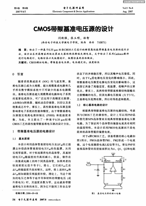
比较精 确 的 电压 ,但 其 电源 电压 较 高 ( 于3V , 大 ) 且 基准 电压范 围有 限 .所 以有 待改进 和提 高 。
1 . 核 心 基 准 电 路 的 设 计 2
统集 成芯 片 中。事 实上 ,高 性能 基准 电 压源 直接
影 响着 电子 系统 的性能 和精 度 。 由于带 隙基 准 电
旷
=
低 输 入共 模 电平 。而作 为输 入 级 的 晶体 管P 和 M3 P 4,则 要 求 有 比较 大 的 栅 面 积 以及 最 小 的栅 M 长 ,以降低 运放 的失调 电压 。此 外 ,运 放还 可 以 采用 R } 偿 网络来 获得 足够 的相位 裕度 。 Cb
1 . 电 流 源 设 计 4
维普资讯
第9 卷
第8 期
电手元 器 件 主 用
E e t n cCo o e t D v c p ia in l cr i o mp n n & e i eAp l t s c o
V0 . o 8 1 N . 9 Au .2 0 g 07
状 态下 的齐 纳稳 压管 。所 以其 噪声 电压 很 低 。 同
时 ,由于 舾 电源 电压变 化 的影 响很 小 ,因此 , 受 带 隙基 准 电压源 受 电源 电压变 化 的影 响很 小 ,这
就 使它 具备 了高 稳定 度 、低 温漂 、低 噪声 的主要
优 点 。事 实上 ,虽 然传 统带 隙基 准源 结构 能 输 出
漂 去 补偿 晶体 管 基 射 结 电 压 舾的 负 温 漂 ,从 而 实 现零温 漂 。对 于恒 流源供 电 的 晶体 管 ,其 基射 结 电压 艇随温 度 的升 高 而 减小 。但 是 ,制作 在
一
- 1、下载文档前请自行甄别文档内容的完整性,平台不提供额外的编辑、内容补充、找答案等附加服务。
- 2、"仅部分预览"的文档,不可在线预览部分如存在完整性等问题,可反馈申请退款(可完整预览的文档不适用该条件!)。
- 3、如文档侵犯您的权益,请联系客服反馈,我们会尽快为您处理(人工客服工作时间:9:00-18:30)。
论文题目:带隙基准源电路与版图设计摘要基准电压源具有相对较高的精度和稳定度,它的温度稳定性以及抗噪性能影响着整个系统的精度和性能。
模拟电路使用基准源,或者是为了得到与电源无关的偏置,或者为了得到与温度无关的偏置,其性能好坏直接影响电路的性能稳定,可见基准源是子电路不可或缺的一部分,因此性能优良的基准源是一切电子系统设计最基本和最关键的要求之一,而集成电路版图是为了实现集成电路设计的输出。
本文的主要目的是用BiCMOS工艺设计出基准源电路的版图并对其进行验证。
本文首先介绍了基准电压源的背景发展趋势及研究意义,然后简单介绍了基准电压源电路的结构及工作原理。
接着主要介绍了版图的设计,验证工具及对设计的版图进行验证。
本设计采用40V的0.5u BiCMOS工艺库设计并绘制版图。
仿真结果表明,设计的基准电压源温度变化为-40℃~~85℃,输出电压为2.5V及1.25V。
最后对用Diva 验证工具对版图进行了DRC和LVS验证,并通过验证,表明本次设计的版图符合要求。
关键字:BiCMOS,基准电压源,温度系数,版图ISubject: Research and Layout Design Of Bandgap ReferenceSpecialty: MicroelectronicsName: Zhong Ting (Signature)____Instructor: Liu Shulin (Signature)____ABSTRACTThe reference voltage source with relatively high precision and stability, temperature stability and noise immunity affect the accuracy and performance of the entire system. Analog circuit using the reference source, or in order to get the bias has nothing to do with power, or in order to be independent of temperature, bias, and its performance directly affects the performance and stability of the circuit shows that the reference source is an integral part of the sub-circuit, excellent reference source is the design of all electronic systems the most basic and critical requirements of one of the IC layout in order to achieve the output of integrated circuit design. The main purpose of this paper is the territory of the reference circuit and BiCMOS process to be verified.This paper first introduces the background of the trends and significance of the reference voltage source, and then briefly introduced the structure and working principle of the voltage reference circuit. Then introduces the layout design and verification tools to verify the design of the territory.This design uses a 40V 0.5u BiCMOS process database design and draw the layout.The simulation results show that the design of voltage reference temperature of -40 ° C ~ ~ 85 ° C, the output voltage of 2.5V and 1.25V. Finally, the Diva verification tool on the territory of the DRC and LVS verification, and validated, show that the territory of the design meet the requirements.Keywords: BiCMOS,band gap , temperature coefficient, layoutII目录1 绪论 (1)1.1 背景介绍及发展趋势 (1)1.2 研究意义 (3)1.3 本文主要工作 (4)2 基准电压源电路设计 (5)2.1 基准电压源的分类及特点 (5)2.2 基准电压源的温度特性 (7)2.2.1 负温度系数项V (7)BE2.2.2 正温度系数电压 (7)2.3 基本原理 (8)2.3.1 与温度无关的电路 (8)2.3.2.与电源无关的偏置电路 (8)2.4 基准电压源电路设计 (9)2.4.1 基本原理 (9)2.4.2 运放的设计 (10)2.4.3 带隙核心电路设计 (14)2.5 仿真分析 (15)3 版图设计 (19)3.1 版图设计的基础 (19)3.1.1 集成电路版图设计与掩膜版、制造工艺的关系 (19)3.1.2 版图设计的设计规则 (20)3.1.3 版图通用设计步骤 (23)3.2工艺介绍 (24)3.2.1 常见工艺简介 (24)III3.2.2 BiCMOS工艺 (26)3.3 带隙基准电路的版图设计 (28)3.3.1 版图的分层及连接 (28)3.3.2 版图设计环境介绍 (29)3.3.3 器件及总体版图 (30)4 版图验证 (39)4.1 版图验证概述 (39)4.2 验证工具介绍 (39)4.2.1 Cadence概述 (39)4.2.2 Diva使用介绍 (40)4.3 版图的DRC验证 (44)4.4 版图的LVS验证 (44)5总结 (46)致谢 (48)参考文献 (49)IV1 绪论1.1 背景介绍及发展趋势基准源是模拟与数字系统中的核心模块之一,它被广泛应用于动态存储(DRAM)、闪存(flash memory)以及其他模拟器件中。
其实现方式有电压基准和电流基准。
基准电压源是模数转换器(ADC)、数模转换器(DAC)、线性稳压器和开关稳压器、温度传感器、充电电池保护芯片和通信电路等电路中不可缺少的部分,基准电流源主要作为高性能运算放大器等器件或电路的偏置,也可用于LVDS驱动器和Viterbi解码器。
基准源需要有稳定的工艺、电压和温度系数,并且不需要随着制造工艺的改变而改变。
带隙基准参考源通常是模拟和混合信号处理系统中重要的组成模块,它用来提供高稳定的参考电平和参考电压,对系统的性能起着至关重要的作用。
传统的带隙基准电路利用双极型晶体管的基极—发射极电压V m的负温度系数和不同电流密度下两个双极型晶体管基极—发射极电压的差值的正温度系数相互补偿,使输出电压达到很低的温度漂移。
但实际设计电路中由于运放的失调电压对V m的影响,V m与温度的非线性关系,使传统的带隙基准电路在温度系数、功耗、PSRR等方面无法达到现今集成电路设计的要求。
随着现代如今,带隙基准源在AD/DA、电源芯片、锁相环、高精度的电压表、电流表、欧姆表等领域有着很广泛的应用。
微电子技术和通信技术的发展,集成电路已进入超深亚微米时代,它的发展继续以高速、高集成度、低功耗为目标。
在发展的同时,集成电路逐渐与其它学科和技术相结合,形成新的方向,新的学科或专业,不断改变着传统专业分工的格局,使得SOC系统(System on Chip)越来越复杂。
这对模拟电路基本模块的电压、功耗、精度和速度等, 提出了更高的要求。
传统的带隙基准源电路结构渐渐难以适应设计需求。
近几年,国内外学者都对传统带隙基准源进行了改进,主要集中降低温度系数,提高了PSRR以及使其能工作在低电源电压下,展现出低功耗、低噪声、低温漂、高精度等特性。
国内外对CMOS工艺带隙基准电压源做了大量的研究,最新的技术进展主要体现在以下几个方面。
(1)低温度系数低温度系数的电压基准源对于高分辨率的DAC和ADC尤其重要。
对于一阶补偿的带隙基准源,温度系数通常可以做到10.60ppm/。
C。
为了进一步降低带隙基准的温度系数必须做高阶补偿。
目前出现的高阶补偿技术包括利用MOS管亚阈区v~I特性的补偿的带隙基准电路、利用电阻的温度特性的曲率校正方法、指数曲率补偿方法、温度分段补偿方法等。
(2)低电压工作的电压基准源随着深亚微米集成电路技术的不断发展,集成电路的电源电压越来越低。
带隙基准电压在1.2V左右,所以一般的带隙基准源的工作电压至少在1.2V以上。
采用特殊电路结构的带隙基准源可以工作在1V左右。
采用这些电路结构后主要的工作电压限制通常来自于运放的工作电压,并最终受限于MOS管的阈值电压。
(3)高电源纹波抑制比随着射频集成电路和数字电路的发展以及带基准源在高频电路应用中的推广,电源抑制比成为了基准源在高频及数模混合电路中的一个重要衡量标准。
在数模混合集成电路中,数字电路的噪声可能对模拟电路产生不利的影响。
因此,在混合电路中电压基准源应该在较宽的范围内具有良好的电源电压抑制比性能。
(4)低功耗低功耗是衡量电路性能好坏的指标之一。
作为集成电路的一个基本单元电路,低功耗也一直是基准电压研究发展的一个方向。
集成电路制造工艺主要有双极工艺、CMOS工艺和BiCMOS工艺。
用双极型工艺可以制造出速度高、驱动能力强、模拟精度高的器件,但双极型器件在功耗和集成度方面却无法满足系统集成的要求:而CMOS工艺可以制造出功耗高、集成度高和抗干扰能力强的CMOS器件,但其速度低、驱动能力差,在既要求高集成度又要求高速的领域中也无能为力。
BiCMOS工艺是把双极型器件和CMOS器件同时制作在同一芯片上,它综合了双极器件高跨导、强负载驱动能力和CMOS器件高集成度、低功耗的优点,使其互相取长补短,发挥各自的优点,它给高速、高集成度、高性能的LSI及VLSI的发展开辟了一条新的道路。