STB pannel_msp430G2221
微控制器MSP430G2221IPW14R MSP430G2221
MSP430G2x31MSP430G2x21 SLAS694I–FEBRUARY2010–REVISED DECEMBER2011MIXED SIGNAL MICROCONTROLLERFEATURES•Low Supply-Voltage Range:1.8V to3.6V•16-Bit Timer_A With Two Capture/CompareRegisters•Ultra-Low Power Consumption•Universal Serial Interface(USI)Supporting SPI –Active Mode:220µA at1MHz,2.2Vand I2C(See Table1)–Standby Mode:0.5µA•Brownout Detector–Off Mode(RAM Retention):0.1µA•10-Bit200-ksps A/D Converter With Internal •Five Power-Saving ModesReference,Sample-and-Hold,and Autoscan •Ultra-Fast Wake-Up From Standby Mode in(See Table1)Less Than1µs•Serial Onboard Programming,•16-Bit RISC Architecture,62.5-ns Instruction No External Programming Voltage Needed, Cycle Time Programmable Code Protection by Security •Basic Clock Module Configurations Fuse–Internal Frequencies up to16MHz With•On-Chip Emulation Logic With Spy-Bi-Wire One Calibrated Frequency Interface–Internal Very Low Power Low-Frequency•For Family Members Details,See Table1 (LF)Oscillator•Available in14-Pin Plastic Small-Outline Thin –32-kHz Crystal Package(TSSOP)(PW),14-Pin Plastic Dual –External Digital Clock Source Inline Package(PDIP)(N),and16-Pin QFNPackage(RSA)•For Complete Module Descriptions,See theMSP430x2xx Family User’s Guide(SLAU144)DESCRIPTIONThe Texas Instruments MSP430family of ultra-low-power microcontrollers consists of several devices featuring different sets of peripherals targeted for various applications.The architecture,combined with five low-power modes,is optimized to achieve extended battery life in portable measurement applications.The device features a powerful16-bit RISC CPU,16-bit registers,and constant generators that contribute to maximum code efficiency. The digitally controlled oscillator(DCO)allows wake-up from low-power modes to active mode in less than1µs. The MSP430G2x21/G2x31series is an ultra-low-power mixed signal microcontroller with a built-in16-bit timer and ten I/O pins.The MSP430G2x31family members have a10-bit A/D converter and built-in communication capability using synchronous protocols(SPI or I2C).For configuration details,see Table1.Typical applications include low-cost sensor systems that capture analog signals,convert them to digital values, and then process the data for display or for transmission to a host system.Please be aware that an important notice concerning availability,standard warranty,and use in critical applications of TexasInstruments semiconductor products and disclaimers thereto appears at the end of this data sheet.PRODUCTION DATA information is current as of publication date.Copyright©2010–2011,Texas Instruments Incorporated Products conform to specifications per the terms of the TexasInstruments standard warranty.Production processing does notnecessarily include testing of all parameters.MSP430G2x31MSP430G2x21SLAS694I–FEBRUARY2010–REVISED Table1.Available Options(1)Flash RAM ADC10Package Device BSL EEM Timer_A USI Clock I/O(KB)(B)Channel Type(2) MSP430G2231IRSA1616-QFN MSP430G2231IPW14-121281x TA218LF,DCO,VLO1014-TSSOP MSP430G2231IN1414-PDIP MSP430G2221IRSA1616-QFN MSP430G2221IPW14-121281x TA21-LF,DCO,VLO1014-TSSOP MSP430G2221IN1414-PDIP MSP430G2131IRSA1616-QFN MSP430G2131IPW14-111281x TA218LF,DCO,VLO1014-TSSOP MSP430G2131IN1414-PDIP MSP430G2121IRSA1616-QFN MSP430G2121IPW14-111281x TA21-LF,DCO,VLO1014-TSSOP MSP430G2121IN1414-PDIP (1)For the most current package and ordering information,see the Package Option Addendum at the end of this document,or see the TIweb site at .(2)Package drawings,thermal data,and symbolization are available at /packaging.2Submit Documentation Feedback Copyright©2010–2011,Texas Instruments IncorporatedDVCCP1.6/TA0.1/SDO/SCL/TDI/TCLKP1.7/SDI/SDA/TDO/TDIRST/NMI/SBWTDIO TEST/SBWTCK XOUT/P2.7XIN/P2.6/TA0.1DVSSP1.0/TA0CLK/ACLKP1.1/TA0.0P1.2/TA0.1P1.3P1.4/SMCLK/TCK P1.5/TA0.0/SCLK/TMSP 1.4/S M C L K /T C KP 1.5/T A 0.0/S C L K /T M SP 1.6/T A 0.1/S D O /S C L /T D I /T C L KP 1.7/S D I /S D A /T D O /T D ID V S SD V S SD V C CD V C CP1.0/TA0CLK/ACLKP1.1/TA0.0P1.2/TA0.1P1.3XIN/P2.6/TA0.1XOUT/P2.7TEST/SBWTCK RST/NMI/SBWTDIOMSP430G2x31MSP430G2x21SLAS694I –FEBRUARY 2010–REVISED DECEMBER 2011Device Pinout,MSP430G2x21N OR PW PACKAGE(TOP VIEW)NOTE:See port schematics in Application Information for detailed I/O information.RSA PACKAGE (TOP VIEW)NOTE:See port schematics in Application Information for detailed I/O information.Copyright ©2010–2011,Texas Instruments Incorporated Submit Documentation Feedback 3DVCCP1.6/TA0.1/A6/SDO/SCL/TDI/TCLKP1.7/A7/SDI/SDA/TDO/TDIRST/NMI/SBWTDIOTEST/SBWTCK XOUT/P2.7XIN/P2.6/TA0.1DVSSP1.0/TA0CLK/ACLK/A0P1.1/TA0.0/A1P1.2/TA0.1/A2P1.3/ADC10CLK/A3/VREF-/VEREF-P1.4/SMCLK/A4/VREF+/VEREF+/TCKP1.5/TA0.0/A5/SCLK/TMSP 1.4/S M C L K /A 4/V R E F +/V E R E F +/T C P 1.5/T A 0.0/S C L K /A 5/T M SP 1.6/T A 0.1/S D O /S C L /T D I /T C L KP 1.7/S D I /S D A /T D O /T D D V S SD V S SD V C CD V C CP1.1/TA0.0/A1P1.2/TA0.1/A2P1.3/ADC10CLK/A3/VREF-/VEREF-MSP430G2x31MSP430G2x21SLAS694I –FEBRUARY 2010–REVISED DECEMBER 2011Device Pinout,MSP430G2x31N OR PW PACKAGE(TOP VIEW)NOTE:See port schematics in Application Information for detailed I/O information.RSA PACKAGE (TOP VIEW)NOTE:See port schematics in Application Information for detailed I/O information.4Submit Documentation FeedbackCopyright ©2010–2011,Texas Instruments IncorporatedDVCCDVSSP1.x XIN XOUTP2.xDVCCDVSSP1.x XIN XOUTP2.xMSP430G2x31MSP430G2x21SLAS694I –FEBRUARY 2010–REVISED DECEMBER 2011Functional Block Diagram,MSP430G2x21Functional Block Diagram,MSP430G2x31Copyright ©2010–2011,Texas Instruments Incorporated Submit Documentation Feedback 5MSP430G2x31MSP430G2x21SLAS694I–FEBRUARY2010–REVISED Table2.Terminal FunctionsTERMINALNO.I/O DESCRIPTIONNAMEN,PW RSAP1.0/General-purpose digital I/O pinTA0CLK/Timer0_A,clock signal TACLK input21I/OACLK/ACLK signal outputA0ADC10analog input A0(1)P1.1/General-purpose digital I/O pinTA0.0/32I/O Timer0_A,capture:CCI0A input,compare:Out0outputA1ADC10analog input A1(1)P1.2/General-purpose digital I/O pinTA0.1/43I/O Timer0_A,capture:CCI1A input,compare:Out1outputA2ADC10analog input A2(1)P1.3/General-purpose digital I/O pinADC10CLK/ADC10,conversion clock output(1)54I/OA3/ADC10analog input A3(1)VREF-/VEREF ADC10negative reference voltage(1)P1.4/General-purpose digital I/O pinSMCLK/SMCLK signal outputA4/65I/O ADC10analog input A4(1)VREF+/VEREF+/ADC10positive reference voltage(1)TCK JTAG test clock,input terminal for device programming and testP1.5/General-purpose digital I/O pinTA0.0/Timer0_A,compare:Out0outputA5/76I/O ADC10analog input A5(1)SCLK/USI:clock input in I2C mode;clock input/output in SPI modeTMS JTAG test mode select,input terminal for device programming and testP1.6/General-purpose digital I/O pinTA0.1/Timer0_A,capture:CCI1A input,compare:Out1outputA6/ADC10analog input A6(1)87I/OSDO/USI:Data output in SPI modeSCL/USI:I2C clock in I2C modeTDI/TCLK JTAG test data input or test clock input during programming and testP1.7/General-purpose digital I/O pinA7/ADC10analog input A7(1)SDI/98I/O USI:Data input in SPI modeSDA/USI:I2C data in I2C modeTDO/TDI(2)JTAG test data output terminal or test data input during programming and testXIN/Input terminal of crystal oscillatorP2.6/1312I/O General-purpose digital I/O pinTA0.1Timer0_A,compare:Out1outputXOUT/Output terminal of crystal oscillator(3)1211I/OP2.7General-purpose digital I/O pinRST/ResetNMI/109I Nonmaskable interrupt inputSBWTDIO Spy-Bi-Wire test data input/output during programming and testTEST/Selects test mode for JTAG pins on Port1.The device protection fuse is connected to TEST.1110ISBWTCK Spy-Bi-Wire test clock input during programming and testDVCC115,16NA Supply voltageDVSS1413,14NA Ground referenceQFN Pad-Pad NA QFN package pad connection to V SS recommended.(1)MSP430G2x31only(2)TDO or TDI is selected via JTAG instruction.(3)If XOUT/P2.7is used as an input,excess current will flow until P2SEL.7is cleared.This is due to the oscillator output driver connectionto this pad after reset.6Submit Documentation Feedback Copyright©2010–2011,Texas Instruments IncorporatedProgram Counter PC/R0Stack Pointer SP/R1Status Register SR/CG1/R2Constant Generator CG2/R3General-Purpose Register R4General-Purpose Register R5General-Purpose Register R6General-Purpose Register R7General-Purpose Register R8General-Purpose Register R9General-Purpose Register R10General-Purpose Register R11General-Purpose Register R12General-Purpose Register R13General-Purpose RegisterR15General-Purpose Register R14MSP430G2x31MSP430G2x21SLAS694I –FEBRUARY 2010–REVISED DECEMBER 2011SHORT-FORM DESCRIPTIONCPUThe MSP430CPU has a 16-bit RISC architecture that is highly transparent to the application.All operations,other than program-flow instructions,are performed as register operations in conjunction with seven addressing modes for source operand and four addressing modes for destination operand.The CPU is integrated with 16registers that provide reduced instruction execution time.The register-to-register operation execution time is one cycle of the CPU clock.Four of the registers,R0to R3,are dedicated as program counter,stack pointer,status register,and constant generator,respectively.The remaining registers are general-purpose registers.Peripherals are connected to the CPU using data,address,and control buses,and can be handled with all instructions.The instruction set consists of the original 51instructions with three formats and seven address modes and additional instructions for the expanded address range.Each instruction can operate on word and byte data.Instruction SetThe instruction set consists of 51instructions with three formats and seven address modes.Each instruction can operate on word and byte data.Table 3shows examples of the three types of instruction formats;Table 4shows the address modes.Table 3.Instruction Word FormatsINSTRUCTION FORMAT SYNTAX OPERATION Dual operands,source-destination ADD R4,R5R4+R5--->R5Single operands,destination only CALL R8PC -->(TOS),R8-->PC Relative jump,un/conditionalJNEJump-on-equal bit =0Table 4.Address Mode Descriptions (1)ADDRESS MODES D SYNTAX EXAMPLE OPERATION Register ✓✓MOV Rs,Rd MOV R10,R11R10---->R11Indexed✓✓MOV X(Rn),Y(Rm)MOV 2(R5),6(R6)M(2+R5)---->M(6+R6)Symbolic (PC relative)✓✓MOV EDE,TONI M(EDE)---->M(TONI)Absolute ✓✓MOV &MEM,&TCDAT M(MEM)---->M(TCDAT)Indirect✓MOV @Rn,Y(Rm)MOV @R10,Tab(R6)M(R10)---->M(Tab+R6)M(R10)---->R11Indirect autoincrement✓MOV @Rn+,Rm MOV @R10+,R11R10+2---->R10Immediate✓MOV #X,TONIMOV #45,TONI #45---->M(TONI)(1)S =source,D =destinationCopyright ©2010–2011,Texas Instruments Incorporated Submit Documentation Feedback 7MSP430G2x31MSP430G2x21SLAS694I–FEBRUARY2010–REVISED Operating ModesThe MSP430has one active mode and five software selectable low-power modes of operation.An interrupt event can wake up the device from any of the low-power modes,service the request,and restore back to the low-power mode on return from the interrupt program.The following six operating modes can be configured by software:•Active mode(AM)–All clocks are active•Low-power mode0(LPM0)–CPU is disabled–ACLK and SMCLK remain active,MCLK is disabled•Low-power mode1(LPM1)–CPU is disabled–ACLK and SMCLK remain active,MCLK is disabled–DCO's dc generator is disabled if DCO not used in active mode•Low-power mode2(LPM2)–CPU is disabled–MCLK and SMCLK are disabled–DCO's dc generator remains enabled–ACLK remains active•Low-power mode3(LPM3)–CPU is disabled–MCLK and SMCLK are disabled–DCO's dc generator is disabled–ACLK remains active•Low-power mode4(LPM4)–CPU is disabled–ACLK is disabled–MCLK and SMCLK are disabled–DCO's dc generator is disabled–Crystal oscillator is stopped8Submit Documentation Feedback Copyright©2010–2011,Texas Instruments IncorporatedMSP430G2x31MSP430G2x21 SLAS694I–FEBRUARY2010–REVISED DECEMBER2011 Interrupt Vector AddressesThe interrupt vectors and the power-up starting address are located in the address range0FFFFh to0FFC0h. The vector contains the16-bit address of the appropriate interrupt handler instruction sequence.If the reset vector(located at address0FFFEh)contains0FFFFh(for example,flash is not programmed)the CPU goes into LPM4immediately after power-up.Table5.Interrupt Sources,Flags,and VectorsSYSTEM WORD INTERRUPT SOURCE INTERRUPT FLAG PRIORITYINTERRUPT ADDRESSPower-Up PORIFGExternal Reset RSTIFGWatchdog Timer+WDTIFG Reset0FFFEh31,highestFlash key violation KEYV(2)PC out-of-range(1)NMI NMIIFG(non)-maskableOscillator fault OFIFG(non)-maskable0FFFCh30 Flash memory access violation ACCVIFG(2)(3)(non)-maskable0FFFAh290FFF8h280FFF6h27 Watchdog Timer+WDTIFG maskable0FFF4h26 Timer_A2TACCR0CCIFG(4)maskable0FFF2h25Timer_A2TACCR1CCIFG,TAIFG(2)(4)maskable0FFF0h240FFEEh230FFECh22 ADC10(5)ADC10IFG(4)(5)maskable0FFEAh21 USI USIIFG,USISTTIFG(2)(4)maskable0FFE8h20 I/O Port P2(two flags)P2IFG.6to P2IFG.7(2)(4)maskable0FFE6h19I/O Port P1(eight flags)P1IFG.0to P1IFG.7(2)(4)maskable0FFE4h180FFE2h170FFE0h16See(6)0FFDEh to15to0,lowest0FFC0h(1)A reset is generated if the CPU tries to fetch instructions from within the module register memory address range(0h to01FFh)or fromwithin unused address ranges.(2)Multiple source flags(3)(non)-maskable:the individual interrupt-enable bit can disable an interrupt event,but the general interrupt enable cannot.(4)Interrupt flags are located in the module.(5)MSP430G2x31only(6)The interrupt vectors at addresses0FFDEh to0FFC0h are not used in this device and can be used for regular program code ifnecessary.Copyright©2010–2011,Texas Instruments Incorporated Submit Documentation Feedback9MSP430G2x31MSP430G2x21SLAS694I–FEBRUARY2010–REVISED Special Function Registers(SFRs)Most interrupt and module enable bits are collected into the lowest address space.Special function register bits not allocated to a functional purpose are not physically present in the device.Simple software access is provided with this arrangement.Legend rw:Bit can be read and written.rw-0,1:Bit can be read and written.It is reset or set by PUC.rw-(0,1):Bit can be read and written.It is reset or set by POR.SFR bit is not present in device.Table6.Interrupt Enable Register1and2Address76543210 00h ACCVIE NMIIE OFIE WDTIErw-0rw-0rw-0rw-0 WDTIE Watchdog Timer interrupt enable.Inactive if watchdog mode is selected.Active if Watchdog Timer is configured in interval timer mode.OFIE Oscillator fault interrupt enableNMIIE(Non)maskable interrupt enableACCVIE Flash access violation interrupt enableAddress76543210 01hTable7.Interrupt Flag Register1and2Address76543210 02h NMIIFG RSTIFG PORIFG OFIFG WDTIFGrw-0rw-(0)rw-(1)rw-1rw-(0) WDTIFG Set on watchdog timer overflow(in watchdog mode)or security key violation.Reset on V CC power-on or a reset condition at the pin in reset mode.OFIFG Flag set on oscillator fault.PORIFG Power-On Reset interrupt flag.Set on V CC power-up.RSTIFG External reset interrupt flag.Set on a reset condition at pin in reset mode.Reset on V CC power-up.NMIIFG Set via pinAddress76543210 03h10Submit Documentation Feedback Copyright©2010–2011,Texas Instruments IncorporatedMemory OrganizationTable8.Memory OrganizationMSP430G2021MSP430G2121MSP430G2221MSP430G2031MSP430G2131MSP430G2231 Memory Size512B1kB2kBMain:interrupt vector Flash0xFFFF to0xFFC00xFFFF to0xFFC00xFFFF to0xFFC0 Main:code memory Flash0xFFFF to0xFE000xFFFF to0xFC000xFFFF to0xF800 Information memory Size256Byte256Byte256ByteFlash010FFh to01000h010FFh to01000h010FFh to01000hRAM Size128B128B128B027Fh to0200h027Fh to0200h027Fh to0200h Peripherals16-bit01FFh to0100h01FFh to0100h01FFh to0100h8-bit0FFh to010h0FFh to010h0FFh to010h8-bit SFR0Fh to00h0Fh to00h0Fh to00hFlash MemoryThe flash memory can be programmed via the Spy-Bi-Wire/JTAG port or in-system by the CPU.The CPU can perform single-byte and single-word writes to the flash memory.Features of the flash memory include:•Flash memory has n segments of main memory and four segments of information memory(A to D)of 64bytes each.Each segment in main memory is512bytes in size.•Segments0to n may be erased in one step,or each segment may be individually erased.•Segments A to D can be erased individually or as a group with segments0to n.Segments A to D are also called information memory.•Segment A contains calibration data.After reset segment A is protected against programming and erasing.It can be unlocked but care should be taken not to erase this segment if the device-specific calibration data is required.Peripherals are connected to the CPU through data,address,and control buses and can be handled using all instructions.For complete module descriptions,see the MSP430x2xx Family User's Guide(SLAU144). Oscillator and System ClockThe clock system is supported by the basic clock module that includes support for a32768-Hz watch crystal oscillator,an internal very-low-power low-frequency oscillator and an internal digitally controlled oscillator(DCO). The basic clock module is designed to meet the requirements of both low system cost and low power consumption.The internal DCO provides a fast turn-on clock source and stabilizes in less than1µs.The basic clock module provides the following clock signals:•Auxiliary clock(ACLK),sourced either from a32768-Hz watch crystal or the internal LF oscillator.•Main clock(MCLK),the system clock used by the CPU.•Sub-Main clock(SMCLK),the sub-system clock used by the peripheral modules.Table9.DCO Calibration Data(Provided From Factory In Flash Information Memory Segment A)CALIBRATIONDCO FREQUENCY SIZE ADDRESSREGISTERCALBC1_1MHZ byte010FFh1MHzCALDCO_1MHZ byte010FEhBrownoutThe brownout circuit is implemented to provide the proper internal reset signal to the device during power on and power off.Digital I/OThere is one8-bit I/O port implemented—port P1—and two bits of I/O port P2:•All individual I/O bits are independently programmable.•Any combination of input,output,and interrupt condition is possible.•Edge-selectable interrupt input capability for all the eight bits of port P1and the two bits of port P2.•Read/write access to port-control registers is supported by all instructions.•Each I/O has an individually programmable pull-up/pull-down resistor.WDT+Watchdog TimerThe primary function of the watchdog timer(WDT+)module is to perform a controlled system restart after a software problem occurs.If the selected time interval expires,a system reset is generated.If the watchdog function is not needed in an application,the module can be disabled or configured as an interval timer and can generate interrupts at selected time intervals.Timer_A2is a16-bit timer/counter with two capture/compare registers.Timer_A2can support multiple capture/compares,PWM outputs,and interval timing.Timer_A2also has extensive interrupt capabilities. Interrupts may be generated from the counter on overflow conditions and from each of the capture/compare registers.Table10.Timer_A2Signal Connections–Device With ADC10INPUT PIN NUMBER MODULE OUTPUT PIN NUMBERDEVICE INPUT MODULE MODULEOUTPUTSIGNAL INPUT NAME BLOCKPW,N RSA PW,N RSASIGNAL2-P1.01-P1.0TACLK TACLKACLK ACLKTimer NASMCLK SMCLK2-P1.01-P1.0TACLK INCLK3-P1.12-P1.1TA0CCI0A3-P1.12-P1.1ACLK(internal)CCI0B7-P1.56-P1.5CCR0TA0VSS GNDVCC VCC4-P1.23-P1.2TA1CCI1A4-P1.23-P1.28-P1.67-P1.6TA1CCI1B8-P1.67-P1.6CCR1TA1VSS GND13-P2.612-P2.6VCC VCCUSIThe universal serial interface(USI)module is used for serial data communication and provides the basic hardware for synchronous communication protocols like SPI and I2C.ADC10(MSP430G2x31only)The ADC10module supports fast,10-bit analog-to-digital conversions.The module implements a10-bit SAR core,sample select control,reference generator and data transfer controller,or DTC,for automatic conversion result handling,allowing ADC samples to be converted and stored without any CPU intervention.Peripheral File MapTable11.Peripherals With Word AccessREGISTERMODULE REGISTER DESCRIPTION OFFSETNAMEADC10(MSP430G2x31only)ADC data transfer start address ADC10SA1BChADC control0ADC10CTL001B0hADC control1ADC10CTL001B2hADC memory ADC10MEM01B4h Timer_A Capture/compare register TACCR10174hCapture/compare register TACCR00172hTimer_A register TAR0170hCapture/compare control TACCTL10164hCapture/compare control TACCTL00162hTimer_A control TACTL0160hTimer_A interrupt vector TAIV012Eh Flash Memory Flash control3FCTL3012ChFlash control2FCTL2012AhFlash control1FCTL10128h Watchdog Timer+Watchdog/timer control WDTCTL0120hTable12.Peripherals With Byte AccessREGISTERMODULE REGISTER DESCRIPTION OFFSETNAMEADC10(MSP430G2x31only)ADC analog enable ADC10AE004AhADC data transfer control1ADC10DTC1049hADC data transfer control0ADC10DTC0048h USI USI control0USICTL0078hUSI control1USICTL1079hUSI clock control USICKCTL07AhUSI bit counter USICNT07BhUSI shift register USISR07Ch Basic Clock System+Basic clock system control3BCSCTL3053hBasic clock system control2BCSCTL2058hBasic clock system control1BCSCTL1057hDCO clock frequency control DCOCTL056h Port P2Port P2resistor enable P2REN02FhPort P2selection P2SEL02EhPort P2interrupt enable P2IE02DhPort P2interrupt edge select P2IES02ChPort P2interrupt flag P2IFG02BhPort P2direction P2DIR02AhPort P2output P2OUT029hPort P2input P2IN028hTable12.Peripherals With Byte Access(continued)REGISTER MODULE REGISTER DESCRIPTION OFFSETNAMEPort P1Port P1resistor enable P1REN027hPort P1selection P1SEL026hPort P1interrupt enable P1IE025hPort P1interrupt edge select P1IES024hPort P1interrupt flag P1IFG023hPort P1direction P1DIR022hPort P1output P1OUT021hPort P1input P1IN020h Special Function SFR interrupt flag2IFG2003hSFR interrupt flag1IFG1002hSFR interrupt enable2IE2001hSFR interrupt enable1IE1000hAbsolute Maximum Ratings(1)Voltage applied at V CC to V SS–0.3V to4.1V Voltage applied to any pin(2)–0.3V to V CC+0.3V Diode current at any device pin±2mAUnprogrammed device–55°C to150°C Storage temperature range,T stg(3)Programmed device–55°C to150°C(1)Stresses beyond those listed under"absolute maximum ratings"may cause permanent damage to the device.These are stress ratingsonly,and functional operation of the device at these or any other conditions beyond those indicated under"recommended operating conditions"is not implied.Exposure to absolute-maximum-rated conditions for extended periods may affect device reliability.(2)All voltages referenced to V SS.The JTAG fuse-blow voltage,V FB,is allowed to exceed the absolute maximum rating.The voltage isapplied to the TEST pin when blowing the JTAG fuse.(3)Higher temperature may be applied during board soldering according to the current JEDEC J-STD-020specification with peak reflowtemperatures not higher than classified on the device label on the shipping boxes or reels.0.01.02.03.04.05.01.52.0 2.53.0 3.54.0V CC −Supply Voltage −V A c t i v e M o d e C u r r e n t −m A0.01.02.03.04.00.04.08.012.016.0f DCO −DCO Frequency −MHzA c t i v e M o d e C u r r e n t −m AElectrical CharacteristicsActive Mode Supply Current Into V CC Excluding External Currentover recommended ranges of supply voltage and operating free-air temperature (unless otherwise noted)(1)(2)PARAMETERTEST CONDITIONST AV CC MINTYP MAXUNITf DCO =f MCLK =f SMCLK =1MHz, 2.2V220f ACLK =32768Hz,Program executes in flash,Active mode (AM)I AM,1MHzBCSCTL1=CALBC1_1MHZ,µAcurrent (1MHz)3V 300370DCOCTL =CALDCO_1MHZ,CPUOFF =0,SCG0=0,SCG1=0,OSCOFF =0(1)All inputs are tied to 0V or to V CC .Outputs do not source or sink any current.(2)The currents are characterized with a Micro Crystal CC4V-T1A SMD crystal with a load capacitance of 9pF.The internal and external load capacitance is chosen to closely match the required 9pF.Typical Characteristics –Active Mode Supply Current (Into V CC )Figure 2.Active Mode Current vs V CC ,T A =25°CFigure 3.Active Mode Current vs DCO Frequency-40I –L o w -P o w e r M o d e C u r r e n t –µAL P M 4T –Temperature –°C A -2020406080I –L o w -P o w e r M o d e C u r r e n t –µAT –Temperature –°CA Low-Power Mode Supply Currents (Into V CC )Excluding External Currentover recommended ranges of supply voltage and operating free-air temperature (unless otherwise noted)(1)(2)PARAMETERTEST CONDITIONST AV CCMINTYP MAX UNITf MCLK =0MHz,f SMCLK =f DCO =1MHz,f ACLK =32768Hz,Low-power mode 0I LPM0,1MHzBCSCTL1=CALBC1_1MHZ,25°C 2.2V 65µA(LPM0)current (3)DCOCTL =CALDCO_1MHZ,CPUOFF =1,SCG0=0,SCG1=0,OSCOFF =0f MCLK =f SMCLK =0MHz,f DCO =1MHz,f ACLK =32768Hz,Low-power mode 2I LPM2BCSCTL1=CALBC1_1MHZ,25°C 2.2V 22µA(LPM2)current (4)DCOCTL =CALDCO_1MHZ,CPUOFF =1,SCG0=0,SCG1=1,OSCOFF =0f DCO =f MCLK =f SMCLK =0MHz,Low-power mode 3f ACLK =32768Hz,I LPM3,LFXT125°C 2.2V 0.7 1.5µA(LPM3)current (4)CPUOFF =1,SCG0=1,SCG1=1,OSCOFF =0f DCO =f MCLK =f SMCLK =0MHz,Low-power mode 3f ACLK from internal LF oscillator (VLO),I LPM3,VLO25°C 2.2V 0.50.7µA current,(LPM3)(4)CPUOFF =1,SCG0=1,SCG1=1,OSCOFF =0f DCO =f MCLK =f SMCLK =0MHz,25°C 2.2V 0.10.5µA Low-power mode 4f ACLK =0Hz,I LPM4(LPM4)current (5)CPUOFF =1,SCG0=1,SCG1=1,85°C2.2V0.81.5µAOSCOFF =1(1)All inputs are tied to 0V or to V CC .Outputs do not source or sink any current.(2)The currents are characterized with a Micro Crystal CC4V-T1A SMD crystal with a load capacitance of 9pF.(3)Current for brownout and WDT clocked by SMCLK included.(4)Current for brownout and WDT clocked by ACLK included.(5)Current for brownout included.Typical Characteristics Low-Power Mode Supply Currentsover recommended ranges of supply voltage and operating free-air temperature (unless otherwise noted)Figure 4.LPM3Current vs Temperature Figure 5.LPM4Current vs TemperatureSchmitt-Trigger Inputs–Ports Pxover recommended ranges of supply voltage and operating free-air temperature(unless otherwise noted)PARAMETER TEST CONDITIONS V CC MIN TYP MAX UNIT0.45V CC0.75V CCV IT+Positive-going input threshold voltage V3V 1.35 2.250.25V CC0.55V CCV IT–Negative-going input threshold voltage V3V0.75 1.65V hys Input voltage hysteresis(V IT+–V IT–)3V0.31VFor pullup:V IN=V SSR Pull Pullup/pulldown resistor3V203550kΩFor pulldown:V IN=V CCC I Input capacitance V IN=V SS or V CC5pF Leakage Current–Ports Pxover recommended ranges of supply voltage and operating free-air temperature(unless otherwise noted)PARAMETER TEST CONDITIONS V CC MIN MAX UNITI lkg(Px.y)High-impedance leakage current(1)(2)3V±50nA(1)The leakage current is measured with V SS or V CC applied to the corresponding pin(s),unless otherwise noted.(2)The leakage of the digital port pins is measured individually.The port pin is selected for input and the pullup/pulldown resistor isdisabled.Outputs–Ports Pxover recommended ranges of supply voltage and operating free-air temperature(unless otherwise noted)PARAMETER TEST CONDITIONS V CC MIN TYP MAX UNIT V OH High-level output voltage I(OHmax)=–6mA(1)3V V CC–0.3VV OL Low-level output voltage I(OLmax)=6mA(1)3V V SS+0.3V (1)The maximum total current,I(OHmax)and I(OLmax),for all outputs combined should not exceed±48mA to hold the maximum voltage dropspecified.Output Frequency–Ports Pxover recommended ranges of supply voltage and operating free-air temperature(unless otherwise noted)PARAMETER TEST CONDITIONS V CC MIN TYP MAX UNITPort output frequencyf Px.y Px.y,C L=20pF,R L=1kΩ(1)(2)3V12MHz(with load)f Port_CLK Clock output frequency Px.y,C L=20pF(2)3V16MHz(1)A resistive divider with2×0.5kΩbetween V CC and V SS is used as load.The output is connected to the center tap of the divider.(2)The output voltage reaches at least10%and90%V CC at the specified toggle frequency.。
MSP430G2231 简介

了解MSP430G2231单片机
一、芯片极限参数 1.电源电压:-0.3V~+4.1V 2.引脚电压:-0.3V~+Vcc+0.3V 3.二极管保护电流: ±2mA
二、一般电气特性 1.阀值电压: ① 高电平输入电压:0.45Vcc~0.75Vcc ② 低电平输入电压:0.25Vcc~0.55Vcc
B
B
N s
V
M 制 测
h
S
I
地
S
三、内部主要资源
数
址
据
总
总
1
R
线
2
A
线
8
M
B
定
看
1
5
时
门
b
1
8通道
i
器
狗
0 A
t
D
b C
i
t
定
并行I/O
计
8
8
P
P
时
数
b
b
1
1
i
i
口
.
器
器
8
t
t
x
/
串
并行I/O
行
通
2
P
U
P
b
2
S
2
接
用
i
口
I
.
2
tHale Waihona Puke x口四、CPU的16个寄存器 R0 程序计数器
R1 堆栈指针
R2 状态寄存器/常量生成寄存器1 R3 常量生成寄存器2 R4 — R15 通用寄存器
五、存储器 1.RAM:
① 00h – 0fh:
② 010h – 0ffh:
MSP430程序库十三硬件乘法器使用资料
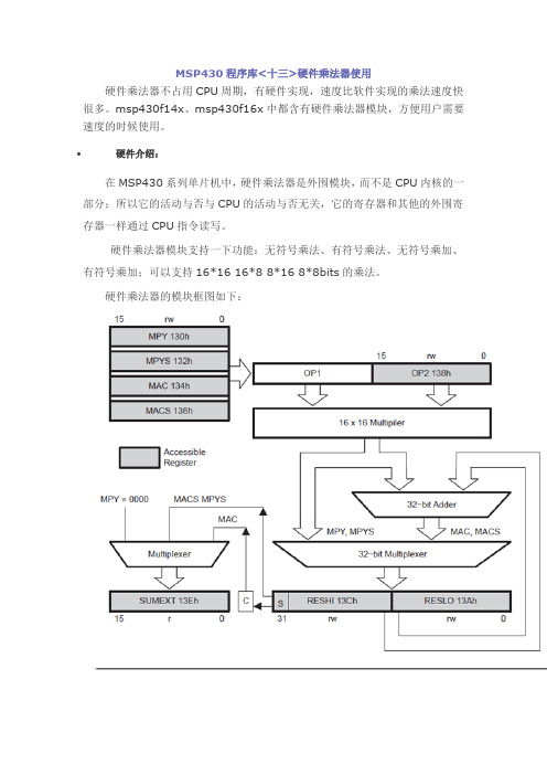
MSP430程序库<十三>硬件乘法器使用硬件乘法器不占用CPU周期,有硬件实现,速度比软件实现的乘法速度快很多。
msp430f14x、msp430f16x中都含有硬件乘法器模块,方便用户需要速度的时候使用。
硬件介绍:在MSP430系列单片机中,硬件乘法器是外围模块,而不是CPU内核的一部分;所以它的活动与否与CPU的活动与否无关,它的寄存器和其他的外围寄存器一样通过CPU指令读写。
硬件乘法器模块支持一下功能:无符号乘法、有符号乘法、无符号乘加、有符号乘加;可以支持16*16 16*8 8*16 8*8bits的乘法。
硬件乘法器的模块框图如下:硬件乘法器模块的四种操作类型(无符号乘法、有符号乘法、无符号乘加、有符号乘加)是由写入的第一个操作数的位置决定的。
这个模块有两个操作数寄存器:OP1和OP2、三个结果寄存器RESLO, RESHI, 和SUMEXT。
RESLO 寄存器存储结果的低字(低16位);RESHI寄存器存储结果的高字(高16位);SUMEXT寄存器存储结果的有关信息。
结果在3个时钟周期后即可完成;写入OP2后的下一条指令即可读取结果,有一种情况例外:用间接寻址方式访问结果。
用间接寻址方式访问结果时,读取结果之前需要有一条NOP指令。
操作数OP1有四个地址(MPY:0130h MPYS:0132h MAC:0134h MACS:0136h),这四个寄存器用来选择乘法的操作模式。
写入第一个操作数寄存器决定用哪种操作:无符号用符号等,但是不启动相乘操作;写入第二个操作数寄存器启动相乘的操作。
计算完成后结果存入寄存器RESLO,RESHI, 和SUMEXT。
操作数1的四个地址对应的操作:四种操作模式下高位结果寄存器的内容如下:四种操作模式SUMEXT 寄存器的内容:连续乘法运算时,如果操作数1不需改变就可以运算,则可以不需要重新写入和以保存内容相同的数;但OP2必须重新写入以启动乘法运算。
MSP430外围模块功能简介[2]
![MSP430外围模块功能简介[2]](https://img.taocdn.com/s3/m/81509783ec3a87c24028c461.png)
基于模拟前端信号处理与控制技术的专业论坛、网站
智拓仪器:www.ourjcdz.com
比较模式:这是该定时 器的默认模式,在此所有的捕获硬件停止工作。如 果此时相应定时器中断允许打开的话,同时开始启动定时器, 定时计数器TAR中的数值等于比较寄存器的值时,则产生中断 请求。如没有中断允许,只是响应的中断标志CCIFGx置位。 同时EQUx 信该号位为真。否则为假 利用它可以控制输出产生占空比可变的PWM波形输出。 当选用了比较模式时: 比较模式常用在用软件设定时中断间隔,来处理有关的事情,如 键盘扫描、事件查询处理、也可结合输出产生脉冲时序发生信号, PWM信号等。 一个典型的例子就是利用不断的装载到TxCCRx中的数据与TAR 的值比较来产生中断处理信号。
基于模拟前端信号处理与控制技术的专业论坛、网站
智拓仪器:www.ourjcdz.com
定时器概念:
定时器的工作过程就象我们的闹钟一样,当闹钟设定在某一时间起 闹后时间就会 开始计时,当达到设定值时就开始起闹。这就是定时处理事物的基本原理。 从这里可以看出定时需要以下几个要素:设定起闹 时间;要有计数的时钟源; 要 有计数到达的终点设置;要有与时间比较的功能;要有比较的结果标志; 要有处理事 物的能力; 要想随时启动和停止定时器开关;在计数方向上可能有增计数还有减计数 (倒计时钟)。 比较就是依据上述定时器的来工作的。只是它的功能很多,如不同的输出波 形、多种时钟源可改变计书数频率 。 在这里定时器的开关是用软件启动就相当闹钟是用手动启动一样。但有时我 们希望有些事物是受外部控制打开的,这就要使定时器还具有捕获功能。捕获功能类 似于外部触发信号来控制内外部事物的精确定位。比如,一个温控系统,当外部温度 达到某一数值时会与内部控制器的设定值比较,产生某种输出状态。而430的捕获是靠 触发沿来控制捕获定时器的计数值。根据计数值来处理事物如前后两次捕获你可以测 量外部事物发声的时间间隔。因此需要有捕获不同信号的能力;要提供捕获的标志和 判断现象的依据(即将计数值复制到捕获寄存器中);要有允许捕获和停止捕获的功 能。 EXIT
Msp430定时器的介绍及其基本应用

Msp430定时器的介绍及其基本应用Msp430定时器的介绍及其基本应用Msp430单片机一共有5种类型的定时器。
看门狗定时器(WDT)、基本定时器(Basic Timer1)、8位定时器/计数器(8-bit Timer/Counter)、定时器A(Timer_A)和定时器B(Timer_B)。
但是这些模块不是所有msp430型号都具有的功能。
1、看门狗定时器(WDT)学过电子的人可能都知道,看门狗的主要功能就是当程序发生故障时能使受控系统重新启动。
msp430中它是一个16位的定时器,有看门狗和定时器两种模式。
2、基本定时器(Basic Timer1)基本定时器是msp430x3xx和msp430F4xx系列器件中的模块,通常向其他外围提供低频控制信号。
它可以只两个8位定时器,也可以是一个16位定时器。
3、8位定时器/计数器(8-bit Timer/Counter)如其名字所示,它是8位的定时器,主要应用在支持串行通信或数据交换,脉冲计数或累加以及定时器使用。
4、16位定时器A和B定时器A在所有msp430系列单片机中都有,而定时器B在msp430f13x/14x和msp430f43x/44x等器件中出现,基本的结构和定时器A是相同的,由于本人最先熟悉并应用的是定时器A所以在这里就主要谈一下自己对定时器A的了解和应用。
定时器A是16位定时器,有4种工作模式,时钟源可选,一般都会有3个可配置输入端的比较/捕获寄存器,并且有8种输出模式。
通过8种输出模式很容易实现PWM波。
定时器A的硬件电路大致可分为2类功能模块:一:计数器TAR计数器TAR是主体,它是一个开启和关闭的定时器,如果开启它就是一直在循环计数,只会有一个溢出中断,也就是当计数由0xffff到0时会产生一个中断TAIFG。
二:比较/捕获寄存器CCRX如何实现定时功能呢?这就要靠三个比较/捕获寄存器了(以后用CCRx表示)。
当计数器TAR的计数值等于CCRx时(这就是捕获/比较中的比较的意思:比较TAR是否等于CCRx),CCRx单元会产生一个中断。
Modicon STB数字输出套件数据表说明书

Product data sheetSpecificationsstandard digital output kit - Modicon STB - 115..230 V AC - 2 OSTBDAO8210KProduct availability : Stock - Normally stocked in distribution facilityMainRange of ProductModicon STB distributed I/O solution Product or Component Type Standard digital output kitKit compositionSTBXTS1100, 5-terminal screw type connector STBDAO8210 moduleSTBXTS2110, 5-terminal spring clamp connector STBXBA2000 base Discrete output number 2Discrete output type Triac Discrete output voltage 115...230 V Discrete output voltage typeACComplementaryDiscrete output current 1000 mA 140 °F (60 °C)2000 mA 86 °F (30 °C)Discrete output logic Positive or negative Output voltage20...265 V AC Absolute maximum voltage 300 V 10 s 400 V 20 ms Response Time 10 ms off-to-on 10.5 ms on-to-off Cold swapping YesHot swapping Yes for standard NIMsFallback State 0 basic NIMsUser configurable standard NIMsProtection typeOutput surge protection varistance and RC circuit Insulation between channels and logic bus1780 V for 1 minuteMaximum leakage current 2 mA at state 0 115 V 2.5 mA at state 0 230 V Surge current 20 A 40 ms 30 A 20 ms Minimum load 5 mAResetManual or automatic reset COM faultProduct CompatibilityI/O base STBXBA2000Power distribution module STBPDT2100/2105D i s c l a i m e r : T h i s d o c u m e n t a t i o n i s n o t i n t e n d e d a s a s u b s t i t u t e f o r a n d i s n o t t o b e u s e d f o r d e t e r m i n i n g s u i t a b i l i t y o r r e l i a b i l i t y o f t h e s e p r o d u c t s f o r s p e c i f i c u s e r a p p l i c a t i o n sSupply Power distribution moduleCurrent consumption45 mA 5 V DC logic busMarking CEOvervoltage category IIStatus LED 1 LED (Green) module status (RDY)1 LED per channel (Green) channel status (OUT1 to OUT2)1 LED (Red) module error (ERR)Height0.72 in (18.4 mm)Depth 2.76 in (70 mm)Width 5.05 in (128.3 mm)Product Weight0.28 lb(US) (0.125 kg)EnvironmentStandards EN/IEC 61131-2Product Certifications ULCSAFM Class 1 Division 2Pollution degree 2 IEC 60664-1Operating altitude<= 6561.68 ft (2000 m)IP degree of protection IP20 conforming to EN 61131-2 class 1Ambient air temperature for32…140 °F (0…60 °C) without derating)operation32...140 °F without deratingAmbient air temperature for-40…185 °F (-40…85 °C) without deratingstorage-40...185 °F without deratingRelative humidity95 % 140 °F (60 °C) without condensationVibration resistance 3 gn 58…150 Hz 35 x 7.5 mm symmetrical DIN rail5 gn 58…150 Hz 35 x 15 mm symmetrical DIN rail+/-0.35 mm 10…58 HzShock resistance30 gn 11 ms IEC 88 reference 2-27Ordering and shipping detailsCategory18215-ADVANTYS STB I/ODiscount Schedule PC32GTIN3595863988925Returnability NoCountry of origin IDPacking UnitsUnit Type of Package 1PCENumber of Units in Package 11Package 1 Height 1.06 in (2.7 cm)Package 1 Width 3.15 in (8.0 cm)Package 1 Length 5.12 in (13.0 cm)Package 1 Weight 5.01 oz (142.0 g)Unit Type of Package 2S02Number of Units in Package 228Package 2 Height 5.91 in (15.0 cm)Package 2 Width11.81 in (30.0 cm)Package 2 Length15.75 in (40.0 cm)Package 2 Weight8.77 lb(US) (3.976 kg)Unit Type of Package 3PALNumber of Units in Package 3448Package 3 Height23.62 in (60.0 cm)Package 3 Width31.50 in (80.0 cm)Package 3 Length176.38 in (448.0 cm)Package 3 Weight140.25 lb(US) (63.616 kg)Offer SustainabilitySustainable offer status Green Premium productCalifornia proposition 65WARNING: This product can expose you to chemicals including: Lead and lead compounds, which isknown to the State of California to cause cancer and birth defects or other reproductive harm. For moreinformation go to REACh Regulation REACh DeclarationEU RoHS Directive Pro-active compliance (Product out of EU RoHS legal scope)EU RoHS DeclarationMercury free YesChina RoHS Regulation China RoHS declarationRoHS exemption information YesEnvironmental Disclosure Product Environmental ProfileCircularity Profile End of Life InformationWEEE The product must be disposed on European Union markets following specific waste collection andnever end up in rubbish bins.Contractual warrantyWarranty18 monthsDimensions Drawings DimensionsConnections and Schema Wiring DiagramExample1 three-wire actuator and 1 two-wire actuatorRecommended replacement(s)。
MSP430G2xx3设备的SMBus库用户指南说明书
SMBus Library for MSP430G2xx3Devices User’s GuideDOCNUM-1.10.00.00Copyright©2015T exas Instruments Incorporated.1 CopyrightCopyright©2015Texas Instruments Incorporated.All rights reserved.MSP430and MSP430Ware are trademarks of Texas Instruments Instruments. ARM and Thumb are registered trademarks and Cortex is a trademark of ARM Limited.Other names and brands may be claimed as the property ofbe aware that an important notice concerning availability,standard warranty,and use in critical applications of Texas Instruments semi-conductor products and disclaimers thereto appears at the end of this document.Texas Instruments13532N.Central Expressway MS3810Dallas,TX75243/Revision InformationThis is version1.10.00.00of this document,last updated on Fri Feb13201511:59:44.Table of Contents2Table of ContentsCopyright (1)Revision Information (1)1Introduction (3)1.1Introduction (3)1.2SMBus (3)1.3The MSP430™SMBus Library Package (4)2Introduction to the MSP430™SMBus API (5)2.1Overview (5)2.2Supported Device Families (5)2.3Supported Development Environments (5)2.4Stack Organization (5)2.5Usage of MCU Peripheral Resources (6)2.6Release Notes and Migration from Previous Versions (6)3SMBus API Usage (7)3.1Introduction (7)3.2Usage (7)3.3Examples (8)IMPORTANT NOTICE (9)1Introduction1.1IntroductionThs SMBus(Sytem Management Bus)API(application programming interface)stack forMSP430™microcontrollers is a turnkey API.It includes support for applications where theMSP430™microcontroller is acting as the master or a slave.The API is designed to minimize the SMBus knowledge required to write an application:All SMBus protocol is handled automatically by the APIThe data interface presented to the application is simple to use,abstracting the applicationfrom SMBus protocolThe user should not need to modify the API source.However,for experienced developers,thesource is open and available for editing.Accessing the API’s source can also be useful for systemdebug.Application examples are included in the MSP430™SMBus Library Package.1.2SMBusThe System Management Bus(SMBus)is a lightweight two-wire interface based on the principlesof I2C,commonly used as a control bus and for power management tasks in computing,mobilecomputing and battery operated applications.A device performing data transfers on the bus canbe considered a master,which is the device which initiates a transaction and drives the clock,or aslave,which is the target of a SMBus transaction driven by the master.Both the master and theslave can act as transmitters or as receivers.SMBus2.0shares a lot of similarities with I2C,but some of the most relevant differences include:Time-out detection when a device stretches the clock for too longPacket Error Checking(PEC)can be optionally appended at the end of each transaction,allowing the bus to automatically validate packetsI2C only defines a PHY and Data-Link layers,but SMBus defines a network layer withdifferent SMBus protocols which can be used to exchange data between devicesOptional use of additional lines such as SMBAlert#and SMBSUS#.For more information about SMBus,please refer to the SMBus2.0specification:/specs/.For more information about I2C,please refer to/documents/user manual/UM10204.pdf1.2.1Supported FeaturesThe following table details the SMBus features supported in the MSP430™SMBus library.SMBus Feature MSP430FR5xx6xx MSP430G2xx3Applicable SMBus2.0 Master Slave Master Slave specification sectionClock Timeout detection1Y es Y es Y es1Y es1 3.1.1.2Manual NACK on invalid address/data N/A Y es2N/A No 4.2Arbitration Y es N/A Y es N/A 4.3.2Clock stretching Y es Y es Y es Y es 4.3.3Multiple Slave address N/A No N/A No 5.2General Call address N/A No N/A No 5.2PEC Y es Y es Y es Y es 5.4Quick Command Partial3Partial3Parial3Partial3 5.5.1Send Byte Y es Y es Y es Y es 5.5.2Receive Byte Y es Y es Y es Y es 5.5.3Write Byte/Word Y es Y es Y es Y es 5.5.4Read Byte/Word Y es Y es Y es Y es 5.5.5Process Call Y es Y es Y es Y es 5.5.6Block Write/Read Y es Y es Y es Y es 5.5.7Block write-block read process call Y es Y es Y es Y es 5.5.8Host notify protocol No No No No 5.5.9ARP No No No No 5.6SMBAlert#No No No No Appendix ASMBSUS#No No No No Appendix ANotes:1.MSP430G2xx3USCI doesn’t have integrated timeout detection and requires a timer2.MSP430FR5x/6xx can optionally-use DMA to stretch SCL while deciding to ACK/NACK thecurrent byte3.Only QuickCommand Write is supported,not QuickCommand Read1.3The MSP430™SMBus Library PackageThis User’s Guide documents the SMBus API and examples.The contents of the package isdescribed below:smbuslib:T op level directory.Contains release notes and the manifestfile related to licensing.•docs:Contains the API and User’s Guides for the supported MSP430™devices•driverlib:Contains the standard MSP430™driverlib which is used in the libraryimplementation for device families that support driverlib(for example,MSP430FR5xx6xx)•examples:Contains the example projects for each of the supported MSP430™devices•src:Contains the source code for the SMBus Library stack2Introduction to the MSP430™SMBus API 2.1OverviewThe MSP430™SMBus API stack allows easy creation of MSP430™applications thatcommunicate with other system components over a SMBus interface.This API supports using the MSP430™microcontroller as the SMBus master or as a SMBusslave.2.2Supported Device FamiliesThe SMBus API stack is supported on the following MSP430™device families:MSP430FR5xx6xxMSP430G2xx32.3Supported Development EnvironmentsThe SMBus API stack and examples build and run on both the IAR and CCS environments forMSP430™microcontrollers.See the Release Notes HTMLfile in the SMBus Library Package forspecific IAR/CCS version information.IAR and CCS are both available in free,code-size-limited versions(8K and16K,respectively,ofobject code).Applications thatfit under8K of memory can be run on both free versions.Applications that are greater than8K cannot be built using the free IAR Kickstart tool.Instead,thefree version of CCS can be used;or a licensed version of either environment.See the Release Notes within the SMBus Library Package zipfile for additional informationspecific to a given release.2.4Stack OrganizationThe software stack is organized into three layers:The public API layer defines the API’s that should be called by application programs.Thesefunctions are defined in smbus.h.The network layer manages the SMBus protocol state machine and interfaces with thephysical layer.These functions are defined in smbus nwk.h and should not be called directlyfrom application programs.The physical layer contain all the device specific code to interact with the MSP430™microcontroller.These functions are defined in smbus phy.h and should not be called directlyfrom application programs.2.5Usage of MCU Peripheral ResourcesWithin the SMBus API,the resources shown below are considered owned by the API.If theapplication accesses them,it should be aware of how the API uses them.2.6Release Notes and Migration from Previous VersionsA Release Notes HTMLfile accompanies each release of the SMBus Library Package.Referencethisfile for any information specific to this release,including:All changes from the previous versionsInstructions for migration from previous versionsUpdated IDE configuration informationKnown issues3SMBus API Usage3.1IntroductionThis chapter contains the detailed documentation for the application API functions anddescriptions on using the API to create a SMBus master or slave application.3.2UsageThis section illustrates the basic application template for master and slave applications.See theexamples for complete applications,and the HTML API documentation for details on theindividual APIs.3.2.1Master Usage Outline//Declare master SMBus structureSMBus SMB;//Initialize GPIOs and clocks...//Initialize GPIO I2C pins...//Initialize SMBus Master always at100kbps per SMBus specSMBus masterInit(&SMB,NULL,(MCLK MHZ*1000000));//Initialize I2C and enable SMBus InterruptsSMBus masterEnableInt(&SMB);//Send SMBus Sendbyte command(0x33)uint8t ret=SMBus masterSendByte(&SMB,//SMB struct0x40,//Slave Addr0x33);//SMB Command...3.2.2Slave Usage Outlinemain(){//Declare slave SMBus structureSMBus SMB;//SMBus receive and transmit buffersuint8t au8RxBuff[SMB MAX PACKET SIZE];uint8t au8TxBuff[SMB MAX PACKET SIZE];//Initialize GPIOs and clocks...//Initialize GPIO I2C pins...//Initialize SMBus SlaveSMBus slaveInit(&SMB,NULL);//Set the slave’s addressSMBus slaveSetAddress(&SMB,0x40);//Set the RX and TX buffers for SMBusSMBus slaveSetRxBuffer(&SMB,au8RxBuff,sizeof(au8RxBuff));SMBus slaveSetTxBuffer(&SMB,au8TxBuff,sizeof(au8TxBuff));//Initialize I2C and enable SMBus InterruptsSMBus slaveEnableInt(&SMB);...while(1){disable interrupt();{BIS SR(LPM3bits+GIE);//Go to sleep}enable interrupt();}//While(1)}#pragma vector=USCIAB0TX VECTOR,USCIAB0RX VECTORinterrupt void USCI ISR(void){//Check the state of SMBusswitch(SMBus slaveProcessInt(&SMB)){case SMBus State Slave QCMD://If a Quick command was detected,execute function(if any)break;case SMBus State Slave CmdComplete://Get command using SMBus slaveGetCommand(&SMB)and process command//if command is not valid/supported//SMBus slaveReportError(&SMB,SMBUS ErrorCode Cmd);LPM3EXIT;//Exit to main loop if requiredbreak;default:break;}//Clear flags to be ready for next packetSMBus processDone(&SMB);}#pragma vector=TIMER1A0VECTORinterrupt void TIMER1A0ISR(void){//Call the SMBUS function to handle a timeout error and restart the SMBUSSMBus slaveProcessTimeoutInt(&SMB);}3.3ExamplesSeveral examples are provided with the release package that illustrate using the library toimplement both SMBus master and slave application.For each example,matching master and slave implementations are provided.ReadByte Echo-sends and echoes back a ReadByte commandWriteWord Dimmer-sends and echoes back a WriteWord commandAllProtocols-sequences through all the SMBus protocolsExamples are configured for the MSP-EXP430G2and MSP-EXP430FR5969launch pad boardsand CCS and IAR projects are provided.9 IMPORTANT NOTICET exas Instruments Incorporated and its subsidiaries(TI)reserve the right to make corrections,modifications,enhancements,improvements, and other changes to its products and services at any time and to discontinue any product or service without notice.Customers should obtain the latest relevant information before placing orders and should verify that such information is current and complete.All products are sold subject to TI’s terms and conditions of sale supplied at the time of order acknowledgment.TI warrants performance of its hardware products to the specifications applicable at the time of sale in accordance with TI’s standard warranty.T esting and other quality control techniques are used to the extent TI deems necessary to support this warranty.Except where mandated by government requirements,testing of all parameters of each product is not necessarily performed.TI assumes no liability for applications assistance or customer product design.Customers are responsible for their products and applications using TI components.T o minimize the risks associated with customer products and applications,customers should provide adequate design and operating safeguards.TI does not warrant or represent that any license,either express or implied,is granted under any TI patent right,copyright,mask work right,or other TI intellectual property right relating to any combination,machine,or process in which TI products or services are used. Information published by TI regarding third-party products or services does not constitute a license from TI to use such products or services or a warranty or endorsement e of such information may require a license from a third party under the patents or other intellectual property of the third party,or a license from TI under the patents or other intellectual property of TI.Reproduction of TI information in TI data books or data sheets is permissible only if reproduction is without alteration and is accom-panied by all associated warranties,conditions,limitations,and notices.Reproduction of this information with alteration is an unfair and deceptive business practice.TI is not responsible or liable for such altered rmation of third parties may be subject to additional restrictions.Resale of TI products or services with statements different from or beyond the parameters stated by TI for that product or service voids all express and any implied warranties for the associated TI product or service and is an unfair and deceptive business practice.TI is not responsible or liable for any such statements.TI products are not authorized for use in safety-critical applications(such as life support)where a failure of the TI product would reasonably be expected to cause severe personal injury or death,unless officers of the parties have executed an agreement specifically governing such use.Buyers represent that they have all necessary expertise in the safety and regulatory ramifications of their applications, and acknowledge and agree that they are solely responsible for all legal,regulatory and safety-related requirements concerning their products and any use of TI products in such safety-critical applications,notwithstanding any applications-related information or support that may be provided by TI.Further,Buyers must fully indemnify TI and its representatives against any damages arising out of the use of TI products in such safety-critical applications.TI products are neither designed nor intended for use in military/aerospace applications or environments unless the TI products are specifically designated by TI as military-grade or“enhanced plastic.”Only products designated by TI as military-grade meet military spec-ifications.Buyers acknowledge and agree that any such use of TI products which TI has not designated as military-grade is solely at the Buyer’s risk,and that they are solely responsible for compliance with all legal and regulatory requirements in connection with such use.TI products are neither designed nor intended for use in automotive applications or environments unless the specific TI products are designated by TI as compliant with ISO/TS16949requirements.Buyers acknowledge and agree that,if they use any non-designated products in automotive applications,TI will not be responsible for any failure to meet such requirements.Following are URLs where you can obtain information on other Texas Instruments products and application solutions:ProductsAmplifiersData ConvertersDLP®ProductsDSPClocks and TimersInterfaceLogicPower Mgmt MicrocontrollersRFIDRF/IF and ZigBee®Solutions amplifi/clockswww.ti-rfi/lprfApplicationsAudioAutomotiveBroadbandDigital ControlMedicalMilitaryOptical NetworkingSecurityT elephonyVideo&ImagingWireless/audio/automotive/broadband/digitalcontrol/medical/military/opticalnetwork/security/telephony/video/wirelessMailing Address:T exas Instruments,Post Office Box655303,Dallas,T exas75265 Copyright©2015,T exas Instruments Incorporated。
MSP430实现的多路电源开关控制器
基于MSP430G2211实现的多路电源开关控制器第一章作品概述 (2)第一节基本情况 (2)第二节软硬件总体设计方案 (2)第二章作品硬件系统设计 (4)第一节MSP430G2系列Launchpad开发板组成及硬件资源情况介绍 (4)第二节关键器件选型以及性能指标参数 (4)第三节单元电路介绍 (5)第五节PCB板设计要求和注意事项 (9)第六节安装调试注意事项 (12)第三章作品软件系统设计 (14)第一节程序流程图介绍 (14)第二节CCS设计与调试方法介绍 (19)第四章总结与思考 (23)第一章作品概述第一节基本情况本作品使用MSP430G2211单片机实现了通过按键对四路功率继电器进行选择控制,达到对四路交流电源加电/断电的控制要求,由于是对220V市电进行控制,所以作品中尽可能的考虑了使用安全问题,使用了隔离电路以及在每一路上都有功率限制。
第二节软硬件总体设计方案系统总体设计框图如下图1.1 系统总体设计框图为了实现安全的控制220V的交流电,本作品使用隔离控制大功率继电器的方式实现。
220V交流电引入系统后,经过继电器和保险管后再经过四路插座输出。
在控制继电器的方式上,为了安全起见,控制信号通过光耦隔离之后控制继电器。
本作品可以实现4路220W 的功率输出控制。
各个模块之间的具体工作关系如下,用户通过键盘像MSP430处理器发送命令,MSP430G2211处理器在检测到案件后,会对相应的继电器控制I/O置位,注意此时的控制信号是隔离之前的信号;此信号经过隔离模块之后交给控制模块,用来控制相应的继电器动作,从而使得不同的通道导通。
第二章作品硬件系统设计第一节MSP430G2系列Launchpad开发板组成及硬件资源情况介绍MSP430G2系列Launchpad是TI推出的一款低成本的开发平台。
它适用于适用于TI 最新MSP430G2xx 系列产品其基于USB 的集成型仿真器可提供为全系列MSP430G2xx 器件开发应用所必需的所有软、硬件。
基于MSP430G2231实现的多路数据采集器
目录第一章作品概述 (2)第一节作品功能和单片机介绍 (2)第二节设计方案 (2)第二章硬件系统设计 (3)第一节 MSP430G2系列Launchpad开发板介绍 (3)第二节信号调理及电源供电电路介绍 (4):电源供电电路 (4):信号调理电路 (5)第三节显示部分电路 (6)第四节硬件装配图 (7)第五节模拟信号调理版PCB图 (9)第三章软件系统设计 (10)第一节程序概述 (10)第二节子程序介绍 (10)第一章作品概述第一节作品功能和单片机介绍运用MSP430G2231型单片机对外部输入的8路电流信号进行顺序采样,并通过12864进行显示。
本作品选用MSP430G2231单片机,该单片机超低功耗,具有5种节电模式,1us内便可从待机模式唤醒,并具有一个强大的16位RISC CPU、16位寄存器和常数发生器,有助于最大限度的发挥代码效率。
此单片机还具有丰富的时钟源,包括LF、OSC和VLO。
它可通过串行口系统编程,无需外部编程电压,具有可编程的保密熔丝代码保护,它具有Spy-Bi-Wire仿真逻辑接口。
另外它还有10位IO口、8个比较器通道和16位的Timer_A定时器,带2路捕获和比较寄存器。
此单片机的IO口和Timer_A定时器都具有强大的中断能力。
第二节设计方案图系统组成结构框图如图所示:外部信号通过模拟信号调理电路将外界输入的4~20mA电流转换成0~的电压信号用ADC10模块进行采集通过单片机的内部运算将电压信号转换成需要显示的电流信号。
模拟信号调理版由采样电阻,低通滤波以及射极跟随器组成。
采样电阻将输入的电流信号转换成电压信号,低通滤波减少存在于输入端的共模干扰,射极跟随器起到减小输出阻抗以及保护后级电路的作用。
模拟信号调理版将输入的4~20mA电流信号转换成~的电压信号通过单片机进行采集。
采集完成后送往点阵液晶进行显示。
该应用充分发挥了MSP430G2231的IO资源:14(总管脚数)=2(电源和地)+2(JTAG)+2(串行点阵)+8(ADC输入)。
MSP430 入门及常见问题解答
MSP430 入门及常见问题解答MSP430 入门及常见问题解答Ver 0.1 - Jeffrey1.MSP430 入门 2. 如何为我的应用选择最合适的 MSP430 芯片? 3.与 MSP430 的引导加载程序通信的开发工具 4.MSP430 需配合何种晶振工作? 5. 使用哪款 MSP430 编程器可以用来烧断 JTAG 熔丝? 6.要实现 MSP430 编程,应如何连接 JTAG? 7.是否有关于 MSP430 的讨论小组或论坛? 8.使用 FET 时需要哪几根 MSP430 JTAG 信号 线? 9.MSP430 的 I/O 口的灌出和吸入电流能力 10.MSP430 仿真器(FET)的常见问题 11.通过启动加载程序(Bootstrap Loader,以下简 称 BSL)为 MSP430 编程 12.MSP430 I2C 模块的速度 13.MSP430 的 USART 的硬件配置 14.MSP430 Flash 数据保持率 15.MSP430 SPI 或 UART 的速度 16.MSP430 Flash 的写入/擦除周期数 17.MSP430 ADC12 模块的通道数 18.MSP430 哪些端口的引脚具有中断能力? 19.MSP430 的全部操作码(记忆规则)列表 20.怎样降低 MSP430 的功耗? 21.MSP430 开发工具支持哪些操作系统? 22.MSP430 DCO 的频率会抖动吗? 23.MSP430 的 Flash 块写(BLKWRT)模式的使 用 24.MSP430 外部中断输入所需的最小脉冲宽度 25.MSP430 的嵌套中断 26.MSP430 端口中断类型 27.除 32.768kHz 晶振,MSP430 还可以配合多 高频率的晶振工作? 28.MSP430 的静电效应值 29.批量生产时对 Flash 编程的方法。
30.MSP430 在上电清除(PUC)和上电复位 ( POR)时初始状态是什么? 31.MSP430 的操作和储存温度范围 32.MSP430 数据存储器的扩展 33.MSP430 的指令周期和长度 34.MSP430 的静电保护二极管 35.在哪能够找到一个 BSDL 文件来建立 JTAG 链 36. IAR Embedded Workbench 提示的错误信息: “unable to open file `cl430`” 37. USART 模块同时工作在 UART 和 SPI 模 使 式 38.系统内部 Flash 的编程及作为 EEPROM 的 使用 39.多个外部中断同时发生的处理 40.FET 支持的芯片封装类型 41.MSP430F11x1 和 MSP430F11x1A 的区别 42.使用两个管脚进行 Flash 升级 43.MSP430x4xx 低功耗晶振的配置 44. 哪一款编程器可以将用户的程序下载到 Flash 中? 45.使用 MSP430 串口编程工具 MSP-PRGS430 的问题 46.在 MSP430 BSL 通信中 80h 的使用 47.MSP430 ADC12 模块的信息源 48.使用 MSP430 Basic Clock 模块中稳定 DCO 频率 49.MSP430 的 I/O 引脚和 JTAG 引脚的复用 50.MSP430 ADC12 的速度 51.MSP430 ADC12 的基准电压引脚的连接 52.MSP430 ADC12 模块的外部电容需求 53.在哪里可以买到 MSP430 的插座 54.MSP430 工作在 8MHz 时推荐的工作电压 55.查找应用报告中的参考文件1.MSP430 的入门 . 要获取关于 MSP430 产品系列的完整信息, 请参看 MSP430 的主页 在 MSP430 主页中,有相关的链接:所有的文档、应用报告、可下载的源代码示例、开 发人员信息。