MCP16251T芯片PDF资料
MEMORY存储芯片MAX1615EUK+T中文规格书
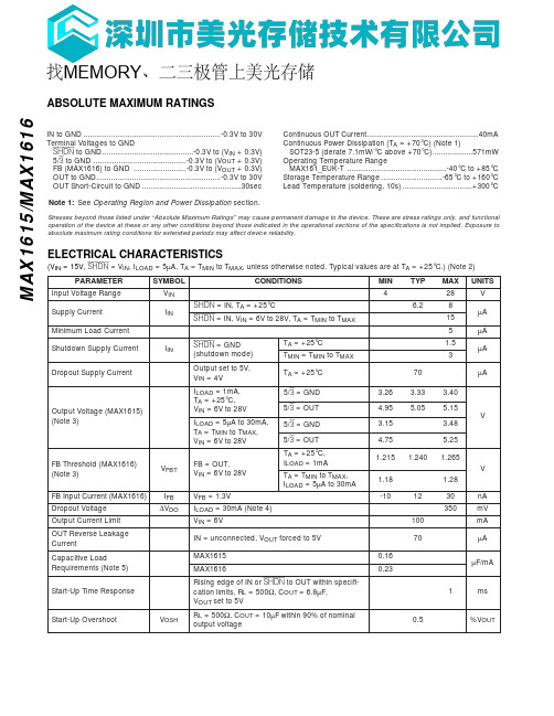
M A X 1615/M A X 1616ABSOLUTE MAXIMUM RATINGSELECTRICAL CHARACTERISTICS(V IN = 15V, SHDN = V IN , I LOAD = 5µA, T A = T MIN to T MAX , unless otherwise noted. Typical values are at T A = +25°C.) (Note 2)Stresses beyond those listed under “Absolute Maximum Ratings” may cause permanent damage to the device. These are stress ratings only, and functional operation of the device at these or any other conditions beyond those indicated in the operational sections of the specifications is not implied. Exposure to absolute maximum rating conditions for extended periods may affect device reliability.IN to GND.................................................................-0.3V to 30V Terminal Voltages to GND SHDN to GND...........................................-0.3V to (V IN + 0.3V)5/3to GND ............................................-0.3V to (V OUT + 0.3V)FB (MAX1616) to GND .........................-0.3V to (V OUT + 0.3V)OUT to GND...........................................................-0.3V to 30V OUT Short-Circuit to GND...............................................30sec Continuous OUT Current.....................................................40mA Continuous Power Dissipation (T A = +70°C) (Note 1)SOT23-5 (derate 7.1mW/°C above +70°C)...................571mW Operating Temperature Range MAX161_EUK-T ...............................................-40°C to +85°C Storage Temperature Range.............................-65°C to +160°C Lead Temperature (soldering, 10s).................................+300°CNote 1:See Operating Region and Power Dissipation section.找MEMORY 、二三极管上美光存储_______________Detailed Description The MAX1615/MAX1616 low-quiescent-current linear regulators are designed primarily for high input voltage applications. The MAX1615 supplies a preselected 3.3V or 5.0V output for loads up to 30mA. The MAX1616provides an adjustable voltage from 1.24V to 28V. The maximum output current is a function of the package’s maximum power dissipation for a given temperature. A 5µA load is required to maintain output regulation.The MAX1615’s output voltage is fed back through aninternal resistor voltage divider connected to OUT. Setthe output voltage to either 3.3V or 5.0V with the 5/3pin.Select the 5V output by connecting 5/3to OUT, or the3.3V output by connecting 5/3to GND.The MAX1616 uses external feedback, allowing the out-put voltage to be set by external resistors (see Settingthe MAX1616 Output Voltage section). The typical FBthreshold is at 1.24V.ShutdownThe device enters shutdown mode when SHDN is low.In shutdown mode, the pass transistor, control circuit,reference, and all biases turn off, reducing the supplycurrent to below 1µA. Connect SHDN to IN for automaticstart-up.Current LimitOutput current is limited to 100mA (typical). The currentlimit exceeds the 30mA (max) safe operating limit. Theoutput can be shorted to ground for 30 seconds withoutdamaging the part.Thermal-Overload Protection When the junction temperature exceeds T J = +150°C,the thermal sensor sends a signal to the shutdownlogic, turning off the pass transistor and allowing the ICto cool. The thermal sensor turns the pass transistor on again after the IC’s junction temperature cools by +20°C (typical), resulting in a pulsating output during continuous thermal-overload conditions.Operating Region and Power Dissipation Maximum power dissipation depends on the thermal resistance of the case and circuit board, the tempera-ture difference between the die junction and ambientair, and the rate of air flow. The device’s power dissipa-MAX1615/MAX1616High-Voltage, Low-Power Linear Regulators for Notebook Computers _______________________________________________________________________________________5______________________________________________________________Pin DescriptionFigure 1. Functional Diagram。
XR16M2550资料
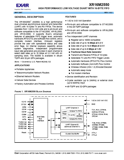
XR16M2550HIGH PERFORMANCE LOW VOLTAGE DUART WITH 16-BYTE FIFO MAY 2007REV. 1.0.2GENERAL DESCRIPTIONThe XR16M25501 (M2550) is a high performance dual universal asynchronous receiver and transmitter (UART) with 16 bytes TX and RX FIFOs. The device operates from 1.62 to 3.63 volts and is pin-to-pin and software compatible to the ST16C2550, XR16L2550, and XR16V2550. It supports Exar’s enhanced features of selectable FIFO trigger level, automatic hardware (RTS/CTS) and software flow control, and a complete modem interface. Onboard registers provide the user with operational status and data error flags. An internal loopback capability allows system diagnostics. Independent programmable baud rate generators are provided in each channel to select data rates up to 16 Mbps at 3.3 Volt with 4X sampling clock. The M2550 is available in 48-pin TQFP and 32-pin QFN packages.N OTE: 1 Covered by U.S. Patent #5,649,122 APPLICATIONS•Portable Appliances•Telecommunication Network Routers•Ethernet Network Routers•Cellular Data Devices•Factory Automation and Process Controls FEATURES•1.62 to 3.63 Volt Operation•Pin-to-pin and software compatible to ST16C2550 in the 48-TQFP package•Pin-to-pin and software compatible to XR16L2550 and XR16V2550•Two independent UART channels■Register set is 16550 compatible■Data rate of up to 16 Mbps at 3.3 V■Data rate of up to 12.5 Mbps at 2.5 V■Data rate of up to 8 Mbps at 1.8V■Fractional Baud Rate Generator■Transmit and Receive FIFOs of 16 bytes■Selectable TX and RX FIFO Trigger Levels■Automatic Hardware (RTS/CTS) Flow Control■Automatic Software (Xon/Xoff) Flow Control■Wireless Infrared (IrDA 1.0) Encoder/Decoder■Automatic sleep mode■Full modem interface•Device Identification and Revision•Crystal oscillator (up to 24MHz) or external clock (up to 64MHz) input•48-TQFP and 32-QFN packagesF IGURE 1. XR16M2550 B LOCK D IAGRAM元器件交易网Exar Corporation 48720 Kato Road, Fremont CA, 94538 • (510) 668-7000 • FAX (510) 668-7017 • XR16M25502HIGH PERFORMANCE LOW VOLTAGE DUART WITH 16-BYTE FIFOREV. 1.0.2F IGURE 2. P IN O UT A SSIGNMENTORDERING INFORMATIONP ART N UMBER P ACKAGE O PERATING T EMPERATURE R ANGED EVICE S TATUSXR16M2550IL3232-Pin QFN -40°C to +85°C Active XR16M2550IM4848-Lead TQFP-40°C to +85°CActiveXR16M25503REV. 1.0.2HIGH PERFORMANCE LOW VOLTAGE DUART WITH 16-BYTE FIFOPIN DESCRIPTIONSPin DescriptionN AME32-QFN P IN #48-TQFP P IN #T YPED ESCRIPTIONDATA BUS INTERFACEA2A1A0181920262728IAddress data lines [2:0]. These 3 address lines select one of the inter-nal registers in UART channel A/B during a data bus transaction.D7D6D5D4D3D2D1D0213231302928273214847464544I/OData bus lines [7:0] (bidirectional).IOR#1419IInput/Output Read Strobe (active low). The falling edge instigates an internal read cycle and retrieves the data byte from an internal register pointed to by the address lines [A2:A0]. The data byte is placed on the data bus to allow the host processor to read it on the rising edge. IOW#1215IInput/Output Write Strobe (active low). The falling edge instigates an internal write cycle and the rising edge transfers the data byte on the data bus to an internal register pointed by the address lines.CSA#710I UART channel A select (active low) to enable UART channel A in the device for data bus operation.CSB#811I UART channel B select (active low) to enable UART channel B in the device for data bus operation.INTA2230OUART channel A Interrupt output. The output state is defined by the user through the software setting of MCR[3]. INTA is set to the active mode and OP2A# output LOW when MCR[3] is set to a logic 1. INTA is set to the three state mode and OP2A# output HIGH when MCR[3] is set to a logic 0 (default). See MCR[3].INTB 2129OUART channel B Interrupt output. The output state is defined by the user through the software setting of MCR[3]. INTB is set to the active mode and OP2B# output LOW when MCR[3] is set to a logic 1. INTB is set to the three state mode and OP2B# output HIGH when MCR[3] is set to a logic 0 (default). See MCR[3].TXRDYA#-43OUART channel A Transmitter Ready (active low). The output provides the TX FIFO/THR status for transmit channel A. See Table 2. If it is not used, leave it unconnected.RXRDYA#-31OUART channel A Receiver Ready (active low). This output provides the RX FIFO/RHR status for receive channel A. See Table 2. If it is not used, leave it unconnected.TXRDYB#-6OUART channel B Transmitter Ready (active low). The output provides the TX FIFO/THR status for transmit channel B. See Table 3. If it is not used, leave it unconnected.XR16M25504HIGH PERFORMANCE LOW VOLTAGE DUART WITH 16-BYTE FIFOREV. 1.0.2RXRDYB#-18OUART channel B Receiver Ready (active low). This output provides the RX FIFO/RHR status for receive channel B. See Table 2. If it is not used, leave it unconnected.MODEM OR SERIAL I/O INTERFACETXA57OUART channel A Transmit Data or infrared encoder data. Standard transmit and receive interface is enabled when MCR[6] = 0. In this mode, the TX signal will be HIGH during reset or idle (no data). Infrared IrDA transmit and receive interface is enabled when MCR[6] = 1. In the Infrared mode, the inactive state (no data) for the Infrared encoder/decoder interface is LOW. If it is not used, leave it unconnected.RXA 45IUART channel A Receive Data or infrared receive data. Normal receive data input must idle HIGH. If this pin is not used, tie it to VCC or pull it high via a 100k ohm resistor.RTSA#2333OUART channel A Request-to-Send (active low) or general purpose out-put. This output must be asserted prior to using auto RTS flow control, see EFR[6], MCR[1], and IER[6].CTSA#2538IUART channel A Clear-to-Send (active low) or general purpose input. It can be used for auto CTS flow control, see EFR[7], and IER[7]. This input should be connected to VCC when not used.DTRA#-34O UART channel A Data-Terminal-Ready (active low) or general purpose output. If it is not used, leave it unconnected.DSRA#-39IUART channel A Data-Set-Ready (active low) or general purpose input. This input should be connected to VCC when not used. This input has no effect on the UART.CDA#-40IUART channel A Carrier-Detect (active low) or general purpose input. This input should be connected to VCC when not used. This input has no effect on the UART.RIA#-41IUART channel A Ring-Indicator (active low) or general purpose input. This input should be connected to VCC when not used. This input has no effect on the UART.OP2A#-32OOutput Port 2 Channel A - The output state is defined by the user and through the software setting of MCR[3]. INTA is set to the active mode and OP2A# output LOW when MCR[3] is set to a logic 1. INTA is set to the three state mode and OP2A# output HIGH when MCR[3] is set to a logic 0. See MCR[3]. If INTA is used, this output should not be used as a general output else it will disturb the INTA output functionality.TXB 68OUART channel B Transmit Data or infrared encoder data. Standard transmit and receive interface is enabled when MCR[6] = 0. In this mode, the TX signal will be HIGH during reset or idle (no data). Infrared IrDA transmit and receive interface is enabled when MCR[6] = 1. In the Infrared mode, the inactive state (no data) for the Infrared encoder/decoder interface is LOW. If it is not used, leave it unconnected.RXB 34IUART channel B Receive Data or infrared receive data. Normal receive data input must idle HIGH. If this pin is not used, tie it to VCC or pull it high via a 100k ohm resistor.Pin DescriptionN AME 32-QFN P IN #48-TQFP P IN #T YPE D ESCRIPTIONXR16M25505REV. 1.0.2HIGH PERFORMANCE LOW VOLTAGE DUART WITH 16-BYTE FIFOPin type: I=Input, O=Output, I/O= Input/output, OD=Output Open Drain.RTSB#1522OUART channel B Request-to-Send (active low) or general purpose out-put. This port must be asserted prior to using auto RTS flow control, see EFR[6], MCR[1], and IER[6].CTSB#1623IUART channel B Clear-to-Send (active low) or general purpose input. It can be used for auto CTS flow control, see EFR[7], and IER[7]. This input should be connected to VCC when not used.DTRB#-35O UART channel B Data-Terminal-Ready (active low) or general purpose output. If it is not used, leave it unconnected.DSRB#-20IUART channel B Data-Set-Ready (active low) or general purpose input. This input should be connected to VCC when not used. This input has no effect on the UART.CDB#-16IUART channel B Carrier-Detect (active low) or general purpose input. This input should be connected to VCC when not used. This input has no effect on the UART.RIB#-21IUART channel B Ring-Indicator (active low) or general purpose input. This input should be connected to VCC when not used. This input has no effect on the UART.OP2B#-9OOutput Port 2 Channel B - The output state is defined by the user and through the software setting of MCR[3]. INTB is set to the active mode and OP2B# output LOW when MCR[3] is set to a logic 1. INTB is set to the three state mode and OP2B# output HIGH when MCR[3] is set to a logic 0. See MCR[3]. If INTB is used, this output should not be used as a general output else it will disturb the INTB output functionality.ANCILLARY SIGNALS XTAL11013I Crystal or external clock input. XTAL21114O Crystal or buffered clock output.RESET2436IReset (active high) - A longer than 40 ns HIGH pulse on this pin will reset the internal registers and all outputs. The UART transmitter output will be held HIGH, the receiver input will be ignored and outputs are reset during reset period (see Table 15).VCC 2642Pwr 2.25V to 3.6V power supply. GND 1317Pwr Power supply common, ground.GNDCenter PadN/APwrThe center pad on the backside of the 32-QFN package is metallic and should be connected to GND on the PCB. The thermal pad size on the PCB should be the approximate size of this center pad and should be solder mask defined. The solder mask opening should be at least 0.0025" inwards from the edge of the PCB thermal pad.NC 9, 1712, 24, 25,37No Connection.Pin DescriptionN AME 32-QFN P IN #48-TQFP P IN #T YPE D ESCRIPTIONXR16M25506HIGH PERFORMANCE LOW VOLTAGE DUART WITH 16-BYTE FIFOREV. 1.0.21.0PRODUCT DESCRIPTIONThe XR16M2550 (M2550) provides serial asynchronous receive data synchronization, parallel-to-serial and serial-to-parallel data conversions for both the transmitter and receiver sections. These functions are necessary for converting the serial data stream into parallel data that is required with digital data systems. Synchronization for the serial data stream is accomplished by adding start and stop bits to the transmit data to form a data character (character orientated protocol). Data integrity is ensured by attaching a parity bit to the data character. The parity bit is checked by the receiver for any transmission bit errors. The electronic circuitry to provide all these functions is fairly complex especially when manufactured on a single integrated silicon chip. The M2550 represents such an integration with greatly enhanced features. The M2550 is fabricated with an advanced CMOS process.Enhanced FeaturesThe XR16M2550 (M2550) integrates the functions of 2 enhanced 16C550 Universal Asynchronous Receiver and Transmitter (UART). Each UART is independently controlled its own set of device configuration registers. The configuration registers set is 16550 UART compatible for control, status and data transfer. Additionally, each UART channel has automatic RTS/CTS hardware flow control, automatic Xon/Xoff and special character software flow control, infrared encoder and decoder (IrDA ver 1.0), programmable baud rate generator with a prescaler of divide by 1 or 4, and data rate up to 16 Mbps at 3.3V with 4X sampling clock rate. The XR16M2550 is a 1.62 V to 3.63 V device.The rich feature set of the M2550 is available through internal registers. Selectable transmit and receive FIFO trigger levels, programmable TX and RX baud rates, and modem interface controls are all standard features. Following a power on reset or an external reset, the M2550 is functionally and software compatible with the previous generation ST16C2550 and XR16L2550. Data RateThe M2550 is capable of operation up to 16 Mbps at 3.3V, 12.5 Mbps at 2.5V and 8 Mbps at 1.8V with 4X sampling rate. The device can operate with an external 24 MHz crystal on pins XTAL1 and XTAL2, or external clock source of up to 64 MHz on XTAL1 pin. With a typical crystal of 14.7456 MHz and through a software option, the user can set the prescaler bit for data rates of up to 3.68 Mbps.The rich feature set of the M2550 is available through the internal registers. Automatic hardware/software flow control, selectable transmit and receive FIFO trigger levels, programmable TX and RX baud rates, infrared encoder/decoder interface, modem interface controls, and a sleep mode are all standard features.XR16M25507REV. 1.0.2HIGH PERFORMANCE LOW VOLTAGE DUART WITH 16-BYTE FIFO2.0FUNCTIONAL DESCRIPTIONS 2.1CPU InterfaceThe CPU interface is 8 data bits wide with 3 address lines and control signals to execute data bus read and write transactions. The M2550 data interface supports the Intel compatible types of CPUs and it is compatible to the industry standard 16C550 UART. No clock (oscillator nor external clock) is required to operate a data bus transaction. Each bus cycle is asynchronous using CS#, IOR# and IOW# signals. Both UART channels share the same data bus for host operations. The data bus interconnections are shown in Figure 3.2.2Device ResetThe RESET input resets the internal registers and the serial interface outputs in both channels to their default state (see Table 15). An active high pulse of longer than 40 ns duration will be required to activate the reset function in the device.2.3Device Identification and RevisionThe XR16M2550 provides a Device Identification code and a Device Revision code to distinguish the part from other devices and revisions. To read the identification code from the part, it is required to set the baud rate generator registers DLL and DLM both to 0x00 (DLD = 0xXX). Now reading the content of the DVID will provide 0x02 for the XR16M2550 and reading the content of DREV will provide the revision of the part; for example, a reading of 0x01 means revision A.2.4Channel A and B SelectionThe UART provides the user with the capability to bi-directionally transfer information between an external CPU and an external serial communication device. A LOW signal on the chip select pins, CSA# or CSB#, allows the user to select UART channel A or B to configure, send transmit data and/or unload receive data to/from the UART. Selecting both UARTs can be useful during power up initialization to write to the same internalF IGURE 3. XR16M2550 D ATA B US I NTERCONNECTIONSXR16M25508HIGH PERFORMANCE LOW VOLTAGE DUART WITH 16-BYTE FIFOREV. 1.0.2registers, but do not attempt to read from both uarts simultaneously. Individual channel select functions are shown in Table 1.2.5Channel A and B Internal RegistersEach UART channel in the M2550 has a set of enhanced registers for control, monitoring and data loading and unloading. The configuration register set is compatible to those already available in the standard single 16C550 and dual ST16C2550. These registers function as data holding registers (THR/RHR), interrupt status and control registers (ISR/IER), a FIFO control register (FCR), receive line status and control registers (LSR/LCR), modem status and control registers (MSR/MCR), programmable data rate (clock) divisor registers (DLL/DLM/DLD), and a user accessible Scratchpad Register (SPR).Beyond the general 16C2550 features and capabilities, the M2550 offers enhanced feature registers (EFR, Xon/Xoff 1, Xon/Xoff 2) that provide automatic RTS and CTS hardware flow control, and Xon/Xoff software flow control. All the register functions are discussed in full detail later in “Section 3.0, UART Internal Registers” on page 21.2.6DMA ModeThe device does not support direct memory access. The DMA Mode (a legacy term) in this document doesn’t mean “direct memory access” but refers to data block transfer operation. The DMA mode affects the state of the RXRDY# A/B and TXRDY# A/B output pins. The transmit and receive FIFO trigger levels provide additional flexibility to the user for block mode operation. The LSR bits 5-6 provide an indication when the transmitter is empty or has an empty location(s) for more data. The user can optionally operate the transmit and receive FIFO in the DMA mode (FCR bit-3=1). When the transmit and receive FIFO are enabled and the DMA mode is disabled (FCR bit-3 = 0), the M2550 is placed in single-character mode for data transmit or receive operation. When DMA mode is enabled (FCR bit-3 = 1), the user takes advantage of block mode operation by loading or unloading the FIFO in a block sequence determined by the selected trigger level. In this mode, the M2550 sets the TXRDY# pin when the transmit FIFO becomes full, and sets the RXRDY# pin when the receive FIFO becomes empty. The following table shows their behavior. Also see Figures 17through 22.T ABLE 1: C HANNEL A AND B S ELECTCSA#CSB#F UNCTION 11UART de-selected 01Channel A selected 10Channel B selected 0Channel A and B selectedT ABLE 2: TXRDY# AND RXRDY# O UTPUTS IN FIFO AND DMA M ODEP INSFCR BIT -0=0(FIFO D ISABLED )FCR B IT -0=1 (FIFO E NABLED )FCR B IT -3 = 0(DMA M ODE D ISABLED )FCR B IT -3 = 1(DMA M ODE E NABLED )RXRDY# A/B LOW = 1 byteHIGH = no dataLOW = at least 1 byte in FIFO HIGH = FIFO emptyHIGH to LOW transition when FIFO reaches the trigger level, or time-out occursLOW to HIGH transition when FIFO empties TXRDY# A/B LOW = THR empty HIGH = byte in THR LOW = FIFO emptyHIGH = at least 1 byte in FIFOLOW = FIFO has at least 1 empty location HIGH = FIFO is fullXR16M25509REV. 1.0.2HIGH PERFORMANCE LOW VOLTAGE DUART WITH 16-BYTE FIFO2.7INTA and INTB OutputsThe INTA and INTB interrupt output changes according to the operating mode and enhanced features setup. Table 3 and 4 summarize the operating behavior for the transmitter and receiver. Also see Figures 17through 22.2.8Crystal Oscillator or External Clock InputThe M2550 includes an on-chip oscillator (XTAL1 and XTAL2) to produce a clock for both UART sections in the device. The CPU data bus does not require this clock for bus operation. The crystal oscillator provides a system clock to the Baud Rate Generators (BRG) section found in each of the UART. XTAL1 is the input to the oscillator or external clock buffer input with XTAL2 pin being the output. For programming details, see ““Section 2.9, Programmable Baud Rate Generator with Fractional Divisor” on page 10.”T ABLE 3: INTA AND INTB P INS O PERATION FOR T RANSMITTERFCR B IT -0 = 0 (FIFO D ISABLED )FCR B IT -0 = 1 (FIFO E NABLED )INTA/B Pin LOW = a byte in THR HIGH = THR empty LOW = FIFO above trigger levelHIGH = FIFO below trigger level or FIFO empty INTA/B PinLOW = a byte in THR HIGH = transmitter emptyLOW = FIFO above trigger levelHIGH = FIFO below trigger level or transmitter emptyT ABLE 4: INTA AND INTB P IN O PERATION F OR R ECEIVERFCR B IT -0 = 0 (FIFO D ISABLED )FCR B IT -0 = 1 (FIFO E NABLED )INTA/B PinLOW = no data HIGH = 1 byteLOW = FIFO below trigger level HIGH = FIFO above trigger levelF IGURE 4. T YPICAL OSCILLATORCONNECTIONSXR16M255010HIGH PERFORMANCE LOW VOLTAGE DUART WITH 16-BYTE FIFOREV. 1.0.2The on-chip oscillator is designed to use an industry standard microprocessor crystal (parallel resonant, fundamental frequency with 10-22 pF capacitance load, ESR of 20-120 ohms and 100 ppm frequency tolerance) connected externally between the XTAL1 and XTAL2 pins (see Figure 4). The programmable Baud Rate Generator is capable of operating with a crystal oscillator frequency of up to 24 MHz. However, with an external clock input on XTAL1 pin, it can extend its operation up to 64 MHz (16 Mbps serial data rate) at 3.3V with an 4X sampling rate. For further reading on the oscillator circuit please see the Application Note DAN108 on the EXAR web site at .2.9Programmable Baud Rate Generator with Fractional DivisorEach UART has its own Baud Rate Generator (BRG) with a prescaler for the transmitter and receiver. The prescaler is controlled by a software bit in the MCR register. The MCR register bit-7 sets the prescaler to divide the input crystal or external clock by 1 or 4. The output of the prescaler clocks to the BRG. The BRG further divides this clock by a programmable divisor between 1 and (216 - 0.0625) in increments of 0.0625 (1/16) to obtain a 16X or 8X or 4X sampling clock of the serial data rate. The sampling clock is used by the transmitter for data bit shifting and receiver for data sampling. The BRG divisor (DLL, DLM and DLD registers) defaults to the value of ’1’ (DLL = 0x01, DLM = 0x00 and DLD = 0x00) upon reset. Therefore, the BRG must be programmed during initialization to the operating data rate. The DLL and DLM registers provide the integer part of the divisor and the DLD register provides the fractional part of the divisor. Only the four lower bits of the DLD are implemented and they are used to select a value from 0 (for setting 0000) to 0.9375 or 15/16 (for setting 1111). Programming the Baud Rate Generator Registers DLL, DLM and DLD provides the capability for selecting the operating data rate. Table 5 shows the standard data rates available with a 24MHz crystal or external clock at 16X clock rate. If the pre-scaler is used (MCR bit-7 = 1), the output data rate will be 4 times less than that shown in Table 5. At 8X sampling rate, these data rates would double. And at 4X sampling rate, they would quadruple. Also, when using 8X sampling mode, please note that the bit-time will have a jitter (+/- 1/16) whenever the DLD is non-zero and is an odd number. When using a non-standard data rate crystal or external clock, the divisor value can be calculated with the following equation(s):The closest divisor that is obtainable in the M2550 can be calculated using the following formula:In the formulas above, please note that:TRUNC (N) = Integer Part of N. For example, TRUNC (5.6) = 5.ROUND (N) = N rounded towards the closest integer. For example, ROUND (7.3) = 7 and ROUND (9.9) = 10.A >> B indicates right shifting the value ’A’ by ’B’ number of bits. For example, 0x78A3 >> 8 = 0x0078.Required Divisor (decimal)=(XTAL1 clock frequency / prescaler) /(serial data rate x 16), with 16X mode, DLD[5:4]=’00’Required Divisor (decimal)= (XTAL1 clock frequency / prescaler / (serial data rate x 8), with 8X mode, DLD[5:4] = ’01’Required Divisor (decimal)= (XTAL1 clock frequency / prescaler / (serial data rate x 4), with 4X mode, DLD[5:4] = ’10’ROUND( (Required Divisor - TRUNC(Required Divisor) )*16)/16 + TRUNC(Required Divisor), whereDLM = TRUNC(Required Divisor) >> 8DLL = TRUNC(Required Divisor) & 0xFFDLD = ROUND( (Required Divisor-TRUNC(Required Divisor) )*16)F IGURE 5. B AUD R ATEG ENERATORT ABLE 5: T YPICAL DATA RATES WITH A 24 MH Z CRYSTAL OR EXTERNAL CLOCK AT 16X S AMPLINGRequired Output DataRate D IVISOR FOR16x Clock(Decimal)D IVISORO BTAINABLE INM2550DLM P ROGRAMV ALUE (HEX)DLL P ROGRAMV ALUE (HEX)DLD P ROGRAMV ALUE (HEX)D ATAE RRORR ATE (%)40037503750E A6002400625625 27100 4800312.5312 8/1613880 9600156.25156 4/1609C40 10000150150 09600 1920078.12578 2/1604E20 250006060 03C00 2880052.083352 1/1603410.04 3840039.062539 1/1602710 500003030 01E00 5760026.041726 1/1601A10.08 750002020 01400 1000001515 0F00 11520013.020813 0D00.16 1536009.76569 12/1609C0.16 2000007.57 8/160780 225000 6.6667 6 11/1606B0.31 230400 6.5104 6 8/160680.16 2500006 6 0600 3000005 5 0500 400000 3.75 3 12/1603C0 460800 3.2552 3 4/160340.16 5000003 3 0300 7500002 2 0200 921600 1.6276 1 10/1601A0.16 1000000 1.5 1 8/1601802.10TransmitterThe transmitter section comprises of an 8-bit Transmit Shift Register (TSR) and 16 bytes of FIFO which includes a byte-wide Transmit Holding Register (THR). TSR shifts out every data bit with the 16X/8X/4X internal clock. A bit time is 16/8/4 clock periods (see DLD). The transmitter sends the start-bit followed by the number of data bits, inserts the proper parity-bit if enabled, and adds the stop-bit(s). The status of the FIFO and TSR are reported in the Line Status Register (LSR bit-5 and bit-6).2.10.1Transmit Holding Register (THR) - Write OnlyThe transmit holding register is an 8-bit register providing a data interface to the host processor. The host writes transmit data byte to the THR to be converted into a serial data stream including start-bit, data bits, parity-bit and stop-bit(s). The least-significant-bit (Bit-0) becomes first data bit to go out. The THR is the input register to the transmit FIFO of 16 bytes when FIFO operation is enabled by FCR bit-0. Every time a write operation is made to the THR, the FIFO data pointer is automatically bumped to the next sequential data location.2.10.2Transmitter Operation in non-FIFO ModeThe host loads transmit data to THR one character at a time. The THR empty flag (LSR bit-5) is set when the data byte is transferred to TSR. THR flag can generate a transmit empty interrupt (ISR bit-1) when it is enabled by IER bit-1. The TSR flag (LSR bit-6) is set when TSR becomes completely empty.F IGURE 6. T RANSMITTER O PERATION IN NON-FIFO M ODE2.10.3Transmitter Operation in FIFO ModeThe host may fill the transmit FIFO with up to 16 bytes of transmit data. The THR empty flag (LSR bit-5) is set whenever the FIFO is empty. The THR empty flag can generate a transmit empty interrupt (ISR bit-1) when the amount of data in the FIFO falls below its selected trigger level. The transmit empty interrupt is enabled by IER bit-1. The TSR flag (LSR bit-6) is set when TSR/FIFO becomes empty.F IGURE 7. T RANSMITTER O PERATION IN FIFO AND F LOW C ONTROL M ODE2.11ReceiverThe receiver section contains an 8-bit Receive Shift Register (RSR) and 16 bytes of FIFO which includes a byte-wide Receive Holding Register (RHR). The RSR uses the 16X/8X/4X clock (DLD[5:4]) for timing. It verifies and validates every bit on the incoming character in the middle of each data bit. On the falling edge of a start or false start bit, an internal receiver counter starts counting at the 16X/8X/4X clock rate. After 8 clocks (or 4 if 8X or 2 if 4X) the start bit period should be at the center of the start bit. At this time the start bit is sampled and if it is still a logic 0 it is validated. Evaluating the start bit in this manner prevents the receiver from assembling a false character. The rest of the data bits and stop bits are sampled and validated in this same manner to prevent false framing. If there were any error(s), they are reported in the LSR register bits 2-4. Upon unloading the receive data byte from RHR, the receive FIFO pointer is bumped and the error tags are immediately updated to reflect the status of the data byte in RHR register. RHR can generate a receive data ready interrupt upon receiving a character or delay until it reaches the FIFO trigger level. Furthermore, data delivery to the host is guaranteed by a receive data ready time-out interrupt when data is not received for 4 word lengths as defined by LCR[1:0] plus 12 bits time. This is equivalent to 3.7-4.6 character times. The RHR interrupt is enabled by IER bit-0. See Figure 8 and Figure 9 below.2.11.1Receive Holding Register (RHR) - Read-OnlyThe Receive Holding Register is an 8-bit register that holds a receive data byte from the Receive Shift Register. It provides the receive data interface to the host processor. The RHR register is part of the receive FIFO of 16 bytes by 11-bits wide, the 3 extra bits are for the 3 error tags to be reported in LSR register. When the FIFO is enabled by FCR bit-0, the RHR contains the first data character received by the FIFO. After the RHR is read, the next character byte is loaded into the RHR and the errors associated with the current data byte are immediately updated in the LSR bits 2-4.。
T-16201中文资料
For other values & Custom Designs, contact factory.Specifications subject to change without notice.15801 Chemical Lane, Huntington Beach, CA 92649-1595Tel: (714) 898-0960 • Fax: (714) 896-0971RhombusIndustries Inc.T1-DP40TurnsOCLC W/W L L DCR Pri.DCR Sec.Part RatioMin.max.max.max.max.Schem.Number + 5%( mH )( pF )( µH )( Ω )( Ω )Style T-162001:1.36CT & 1:2CT 1.2350.60.70.9"3"T-162011:2CT & 1:2CT 1.2350.60.8 1.8"3"T-162021:1:1.26 & 1:2CT 1.2350.60.80.8 / 1.8"2"T-162031:1.15 & 1:2CT 1.2350.60.80.8 / 1.8"1"T-162041:1CT & 1:1CT 1.2350.60.80.8"3"T-162051CT:2CT & 1CT:2CT 1.2350.60.7 1.4"8"T-162061:2CT & 1:1CT 1.2350.60.8 1.8 / 0.8"2"T-162071CT:2CT & 1:1 1.2350.60.70.9"6"T-162081:2CT & 1:1.36 1.2350.60.8 1.8 / 0.8"7"T-162091:1.14CT & 1:2CT 1.2350.60.70.9"3"T-162101:1.36 & 1:2CT 1.2350.60.7 1.0"1"T-162111:1.36 & 1:1.36CT 1.2350.4 / 0.50.7 1.0"1"T-162121:1.15 & 1:1.15 1.2350.60.80.8 / 1.8"5"T-162131:1.14 & 1:1.14CT 1.2350.60.80.8 / 1.8"1"T-162141:2 & 1:2CT 1.2350.60.8 1.8"4"T-162151:2 & 1:2 1.2350.60.8 1.8"5"T-162161CT:1.41 & 1CT:1.41 1.2350.60.8 1.8"3"T-162171:2CT & 1CT:21.2350.60.7 / 1.01.0 / 0.7"3"Electrical Specifications 1, 2 at 25o CT-16200T-16201T-16202T-16203T-16204T-16205T-16206T-16207T-16208T-16209T-16210T-16211T-16212T-16213T-16214T-16215T-16216T-1621728-30, 38-40 / 6-8, 16-186-8, 16-18 / 28-30, 38-401-3, 11-13 / 23-25, 33-351-3, 11-13 / 23-25, 33-356-8, 16-18 / 28-30, 38-406-8, 16-18 / 28-30, 38-401-3, 11-13 / 23-25, 33-351-3, 11-13 / 23-25, 33-3528-30, 38-40 / 6-8, 16-1828-30, 38-40 / 6-8, 16-181-3, 11-13 / 23-25, 33-351-3, 11-13 / 23-25, 33-351-3, 11-13 / 6-8, 16-181-3, 11-13 / 23-25, 33-351-3, 16-18 / 28-30, 33-351-3, 11-13 / 6-8, 16-181-3, 11-13 / 23-25, 33-356-8, 16-18 / 1-3, 11-13P/N Primary PinsNew! T1 / CEPT / ISDN-PRI SMD 40 Pin Quad Modules 4Transformers Per PartFor T1/CEPT/PRI Telecom Applications Designed to meet CCITT and FCC Requirements1500 VRMS Minimum IsolationOCL Tested at 100kHz 50mV Flammability: Materials used in the production of these units meet requirements of UL94-VO and IEC 695-2-2 needle flame test.Dual Port designParts shipped in anti-static tubes.Custom Designs AvailableOther Configurations and Packages Available See Our Web Page Under Data Communications/T1Tape & Reel Available元器件交易网For other values & Custom Designs, contact factory.Specifications subject to change without notice.15801 Chemical Lane, Huntington Beach, CA 92649-1595Tel: (714) 898-0960 • Fax: (714) 896-0971RhombusIndustries Inc.T1-DP40Schematic Style "1"Schematic Style "2"Schematic Style "3"Schematic Style "4"Schematic Style "6"Schematic Style "5"Schematic Style "7"Schematic Style "8"136871113161718283033353839402523291368711131617182830333538344025232413681113161821213687111316181368111316182830333538402523283033353840252313681113161821228303335383940252313681113161821228303335384025232830333538402523121368111316182127172830333538402523373429242940-Pin 50 mil SMD Package Physical Dimensions in inches (mm).620 (15.75).640 (16.26) .485(12.32)MAX..045(1.14)TYP..010(0.25)TYP.1.120(28.45)MAX..016(0.41)TYP..230(5.84)MAX..050(1.27)TYP..010(0.25)TYP.元器件交易网。
14.MCP162_datasheet(稳压芯片)
© 2011 Microchip Technology Inc.DS41420C-page 1MCP1623/24Features:•Up to 96% Typical Efficiency•425mA Typical Peak Input Current Limit:-I OUT > 50mA @ 1.2V V IN , 3.3V V OUT -I OUT > 175mA @ 2.4V V IN , 3.3V V OUT -I OUT > 175mA @ 3.3V V IN, 5.0V V OUT•Low Start-up Voltage: 0.65V, typical 3.3V V OUT @ 1mA•Low Operating Input Voltage: 0.35V, typical 3.3V OUT @ 1mA•Adjustable Output Voltage Range: 2.0V to 5.5V •Maximum Input Voltage ≤ V OUT < 5.5V•Automatic PFM/PWM Operation (MCP1624)•PWM-only Operation (MCP1623)•500kHz PWM Frequency•Low Device Quiescent Current: 19µA, typical PFM mode•Internal Synchronous Rectifier •Internal Compensation•Inrush Current Limiting and Internal Soft-Start •True Load Disconnect•Shutdown Current (All States): < 1µA •Low Noise, Anti-Ringing Control •Overtemperature Protection•SOT-23-6 and 2 x 3 DFN-8 PackageApplications:•One, Two and Three Cell Alkaline and NiMH/NiCd Low-Power PIC ® Microcontroller ApplicationsGeneral Description:The MCP1623/24 is a compact, high-efficiency, fixed frequency, synchronous step-up DC-DC converter. It provides an easy-to-use power supply solution for PIC microcontroller applications powered by either one-cell, two-cell, or three-cell alkaline, NiCd, NiMH,one-cell Li-Ion or Li-Polymer batteries.Low-voltage technology allows the regulator to start-up without high inrush current or output voltage overshoot from a low 0.65V input. High efficiency is accomplished by integrating the low resistance N-Channel Boost switch and synchronous P-Channel switch. All compensation and protection circuitry are integrated to minimize external components. For standby applications, the MCP1624 operates and consumes only 19µA while operating at no load. The MCP1623device option is available that operates in PWM-only mode.A “true” Load Disconnect mode provides input to output isolation while disabled (EN =GND) by removing the normal boost regulator diode path from input to output.This mode consumes less than 1µA of input current.Output voltage is set by a small external resistor divider.Packaging41236V IN V FBSW GND EN 5V OUT MCP1623/246-Lead SOT-23MCP1623/242x3 DFN*P GND S GND EN V OUTS V OUTP 12348765SWV IN V FB EP 9* Includes Exposed Thermal Pad (EP); see Table 3-1.Low-Voltage Input Boost Regulatorfor PIC ® Microcontrollers捷多邦,您值得信赖的PCB打样专家!MCP1623/24FIGURE 1:Typical Application.DS41420C-page 2© 2011 Microchip Technology Inc.MCP1623/241.0ELECTRICALCHARACTERISTICSAbsolute Maximum Ratings †EN, FB, V IN, V SW, V OUT - GND...........................+6.5V EN, FB...........<greater of V OUT or V IN > (GND - 0.3V) Output Short Circuit Current.......................Continuous Power Dissipation ............................Internally Limited Storage Temperature.........................-65o C to +150o C Ambient Temp. with Power Applied......-40o C to +85o C Operating Junction Temperature........-40o C to +125o C ESD Protection On All Pins:HBM........................................................3kVMM........................................................300V † Notice: Stresses above those listed under “Maximum Ratings” may cause permanent damage to the device. This is a stress rating only and functional operation of the device at those or any other conditions above those indicated in the operational sections of this specification is not intended. Exposure to maximum rating conditions for extended periods may affect device reliability.DC CHARACTERISTICSElectrical Characteristics: Unless otherwise indicated, V IN = 1.2V, C OUT = C IN = 10µF, L = 4.7µH, V OUT=3.3V, I OUT=15mA, T A = +25°C.Boldface specifications apply over the T A range of -40o C to +85o C.Parameters Sym.Min.Typ.Max.Units ConditionsInput CharacteristicsMinimum Start-Up Voltage V IN—0.650.8V Note1Minimum Input Voltage AfterStart-UpV IN—0.35—V Note1Output Voltage Adjust Range V OUT 2.0 5.5V V OUT≥ V IN; Note2 Maximum Output Current I OUT50——mA 1.5V V IN, 3.3V V OUT Feedback Voltage V FB 1.120 1.21 1.299V—Feedback Input Bias Current I VFB—10—pA—Quiescent Current – PFM mode I QPFM—1930µA Measured at V OUT = 4.0V;EN = V IN, I OUT = 0mA;Note3Quiescent Current – PWM mode I QPWM—220—µA Measured at V OUT; EN = V INI OUT = 0mA; Note3Quiescent Current – Shutdown I QSHDN—0.7 2.3µA V OUT=EN= GND;Includes N-Channel andP-Channel Switch Leakage NMOS Switch Leakage I NLK—0.31µA V IN=V SW=5V;V OUT =5.5V V EN=V FB=GND PMOS Switch Leakage I PLK—0.050.2µA V IN=VS W=GND;V OUT=5.5VNMOS Switch ON Resistance R DS(ON)N—0.6—ΩV IN = 3.3V, I SW = 100mA PMOS Switch ON Resistance R DS(ON)P—0.9—ΩV IN = 3.3V, I SW = 100mA Note1: 3.3KΩ resistive load, 3.3V OUT (1mA).2:For V IN > V OUT, V OUT will not remain in regulation.3:I Q is measured from V OUT; V IN quiescent current will vary with boost ratio. V IN quiescent current can be estimated by: (I QPFM * (V OUT/V IN)), (I QPWM * (V OUT/V IN)).4:220Ω resistive load, 3.3V OUT (15mA).5:Peak current limit determined by characterization, not production tested.© 2011 Microchip Technology Inc.DS41420C-page 3MCP1623/24DS41420C-page 4© 2011 Microchip Technology Inc.TEMPERATURE SPECIFICATIONSNMOS Peak Switch Current LimitI N(MAX)300425—mA Note 5V OUT Accuracy V OUT %-7.4—+7.4%Includes Line and Load Regulation; V IN = 1.5V I OUT = 50 mA Line Regulation|(ΔV OUT /V OUT ) / ΔV IN |—0.01—%/VV IN = 1.5V to 3V I OUT = 25mALoad Regulation |ΔV OUT / V OUT |—0.01—%I OUT = 25mA to 50mA;V IN = 1.5VMaximum Duty Cycle DC MAX —90—%Switching Frequency f SW 370500630kHzEN Input Logic High V IH 90——%of V IN I OUT = 1mA EN Input Logic Low V IL ——20%of V IN I OUT = 1mA EN Input Leakage Current I ENLK —0.005—µA V EN = 5VSoft-start Time t SS —750—µS EN Low-to-High, 90% of V OUT ; Note 4Thermal Shutdown Die TemperatureT SD —150—°C Die Temperature Hysteresis T SDHYS—10—°CElectrical Specifications:ParametersSym.Min.Typ.Max.UnitsConditionsTemperature RangesOperating Junction Temperature RangeT J -40—+125°C Steady StateStorage Temperature Range T A -65—+150°C Maximum Junction Temperature T J——+150°CTransient Package Thermal Resistance Thermal Resistance, 5L-TSOT23θJA—192—°C/WEIA/JESD51-3 StandardDC CHARACTERISTICS (CONTINUED)Electrical Characteristics: Unless otherwise indicated, V IN = 1.2V, C OUT = C IN = 10µF, L = 4.7µH, V OUT =3.3V, I OUT =15mA, T A = +25°C.Boldface specifications apply over the T A range of -40o C to +85o C.ParametersSym.Min.Typ.Max.Units ConditionsNote 1:3.3K Ω resistive load, 3.3V OUT (1mA).2:For V IN > V OUT , V OUT will not remain in regulation.3:I Q is measured from V OUT ; V IN quiescent current will vary with boost ratio. V IN quiescent current can be estimated by: (I QPFM * (V OUT /V IN )), (I QPWM * (V OUT /V IN )).4:220Ω resistive load, 3.3V OUT (15mA).5:Peak current limit determined by characterization, not production tested.MCP1623/24 2.0TYPICAL PERFORMANCE CURVESNote: Unless otherwise indicated, V IN=EN=1.2V, C OUT=C IN=10µF, L=4.7µH, V OUT=3.3V,I LOAD=15mA, T A=+25°C.OUT Q Temperature in PFM Mode.OUT Q Temperature in PWM Mode.OUTMAX V OUT.I OUT, V OUT = 2.0V.FIGURE 2-5:MCP1624 Efficiency vs.I OUT, V OUT = 3.3V.FIGURE 2-6:MCP1624 Efficiency vs.I OUT, V OUT = 5.0V.Note:The graphs and tables provided following this note are a statistical summary based on a limited number of samples and are provided for informational purposes only. The performance characteristics listed herein arenot tested or guaranteed. In some graphs or tables, the data presented may be outside the specifiedoperating range (e.g., outside specified power supply range) and therefore outside the warranted range.© 2011 Microchip Technology Inc.DS41420C-page 5MCP1623/24DS41420C-page 6© 2011 Microchip Technology Inc.Note: Unless otherwise indicated, V IN =EN =1.2V, C OUT =C IN =10µF, L =4.7µH, V OUT =3.3V,I LOAD =15mA, T A =+25°C.I OUT , V OUT = 2.0V.FIGURE 2-8:MCP1623 Efficiency vs. I OUT , V OUT = 3.3V.I OUT , V OUT = 5.0V.Shutdown V IN into Resistive Load vs. I OUT .OSC Temperature.Skipping Mode Threshold vs. I OUT .© 2011 Microchip Technology Inc.DS41420C-page 7MCP1623/24Note: Unless otherwise indicated, V IN =EN =1.2V, C OUT =C IN =10µF, L =4.7µH, V OUT =3.3V,I LOAD =15mA, T A =+25°C.V IN .R DSON vs. > of V IN or V OUT .Current vs. VIN .FIGURE 2-16:MCP1624 3.3V V OUTPFM Mode Waveforms.FIGURE 2-17:MCP1623 3.3V V OUTPWM Mode Waveforms.FIGURE 2-18:MCP1623/24 High LoadWaveforms.MCP1623/24DS41420C-page 8© 2011 Microchip Technology Inc.Note: Unless otherwise indicated, V IN =EN =1.2V, C OUT =C IN =10µF, L =4.7µH, V OUT =3.3V,I LOAD =15mA, T A =+25°C.FIGURE 2-19: 3.3V Start-up After Enable.FIGURE 2-20: 3.3V Start-up when V IN =V ENABLE .FIGURE 2-21:MCP1624 3.3V V OUT LoadTransient Waveforms.FIGURE 2-22:MCP1623 3.3V V OUT Load Transient Waveforms.FIGURE 2-23:MCP1623 2.0V V OUT LoadTransient Waveforms.FIGURE 2-24: 3.3V V OUT Line TransientWaveforms.MCP1623 PWMMCP1623/243.0PIN DESCRIPTIONSThe descriptions of the pins are listed in Table3-1.TABLE 3-1:PIN FUNCTION TABLE3.1Switch Node Pin (SW)Connect the inductor from the input voltage to the SW pin. The SW pin carries inductor current and can be as high as 425mA peak. The integrated N-Channel switch drain and integrated P-Channel switch source are internally connected at the SW node.3.2Ground Pin (GND)The ground or return pin is used for circuit ground connection. Length of trace from input cap return, output cap return and GND pin should be made as short as possible to minimize noise on the GND pin.3.3Enable Pin (EN)The EN pin is a logic-level input used to enable or disable device switching and lower quiescent current while disabled. A logic high (>90% of V IN) will enable the regulator output. A logic low (<20% of V IN) will ensure that the regulator is disabled.3.4Feedback Voltage Pin (FB)The FB pin is used to provide output voltage regulation by using a resistor divider. The FB voltage will be 1.21V typical with the output voltage in regulation.3.5Output Voltage Pin (V OUT)The output voltage pin connects the integrated P-Channel MOSFET to the output capacitor. The FB voltage divider is also connected to the V OUT pin for voltage regulation.3.6Power Supply Input Voltage Pin(V IN)Connect the input voltage source to V IN. The input source should be decoupled to GND with a 4.7µF minimum capacitor.3.7Signal Ground Pin (S GND)The signal ground pin is used as a return for the integrated V REF and error amplifier. In the 2x3 DFN package, the S GND and power ground (P GND) pins are connected externally.3.8Power Ground Pin (P GND)The power ground pin is used as a return for the high--current N-Channel switch. In the 2x3 DFN package, the P GND and signal ground (S GND) pins are connected externally.3.9Output Voltage Sense Pin (V OUTS) The output voltage sense pin connects the regulated output voltage to the internal bias circuits. In the 2x3 DFN package, V OUTS and V OUTP are connected externally.3.10Output Voltage Power Pin (V OUTP) The output voltage power pin connects the output voltage to the switch node. High current flows through the integrated P-Channel and out of this pin to the output capacitor and output. In the 2x3 DFN package, V OUTS and V OUTP are connected externally.3.11Exposed Thermal Pad (EP)There is an internal electrical connection between the Exposed Thermal Pad (EP) and the V SS pin; they must be connected to the same potential on the Printed Circuit Board (PCB).Pin NameMCP1623/24Description SOT232x3 DFNSW15Switch Node, Boost Inductor Input PinGND2—Ground PinEN34Enable Control Input PinFB41Feedback Voltage PinV OUT5—Output Voltage PinV IN68Input Voltage PinS GND—2Signal Ground PinP GND—3Power Ground PinV OUTS—7Output Voltage Sense PinV OUTP—6Output Voltage Power PinEP—9Exposed Thermal Pad (EP); must be connected to V SS.© 2011 Microchip Technology Inc.DS41420C-page 9MCP1623/24DS41420C-page 10© 2011 Microchip Technology Inc.4.0DETAILED DESCRIPTION4.1Device Option OverviewThe MCP1623/24 family of devices is capable of low start-up voltage and delivers high efficiency over a wide load range for single cell, two cell, three cell alkaline,NiMH, NiCd and single cell Li-Ion battery inputs. A high level of integration lowers total system cost, eases implementation and reduces board area. The devices feature low start-up voltage, adjustable output voltage,PWM/PFM mode operation, low I Q , integrated synchronous switch, internal compensation, low noise anti-ring control, inrush current limit and soft start.There is one feature option for the MCP1623/24 family:PWM/PFM mode or PWM mode only.4.1.1PWM/PFM MODE OPTIONThe MCP1624 devices use an automatic switchover from PWM to PFM mode for light load conditions to maximize efficiency over a wide range of output current.During PFM mode, higher peak current is used to pump the output up to the threshold limit. While operating in PFM or PWM mode, the P-Channel switch is used as a synchronous rectifier, turning off when the inductor current reaches 0 mA to maximize efficiency. In PFM mode, a comparator is used to terminate switching when the output voltage reaches the upper threshold limit.Once switching has terminated, the output voltage will decay or coast down. During this period, very low I Q is consumed from the device and input source, which keeps power efficiency high at light load. The disadvantages of PWM/PFM mode are higher output ripple voltage and variable PFM mode frequency. The PFM mode frequency is a function of input voltage,output voltage and load. While in PFM mode, the boost converter pumps the output up at a switching frequency of 500kHz.4.1.2PWM MODE ONLY OPTIONThe MCP1623 devices disable PFM mode switching,and operate only in PWM mode over the entire load range. During periods of light load operation, the MCP1623 continues to operate at a constant 500kHz switching frequency, keeping the output ripple voltage lower than PFM mode. During PWM-only mode, the MCP1623 P-Channel switch acts as a synchronous rectifier by turning off to prevent reverse current flow from the output cap back to the input in order to keep efficiency high. For noise immunity, the N-Channel MOSFET current sense is blanked for approximately 100ns. With a typical minimum duty cycle of 100ns,the MCP1623 continues to switch at a constant frequency under light load conditions. Figure 2-12represents the input voltage versus load current for the pulse-skipping threshold in PWM-only mode. At lighter loads, the MCP1623 device begins to skip pulses.TABLE 4-1:PART NUMBER SELECTIONPart Number PWM/PFMPWMMCP1624XMCP1623X4.2Functional DescriptionThe MCP1623/24 is a compact, high-efficiency, fixed frequency, step-up DC-DC converter that provides an easy-to-use power supply solution for PIC microcontroller applications powered by either one-cell,two-cell, or three-cell alkaline, NiCd, or NiMH, or one-cell Li-Ion or Li-Polymer batteries.Figure 4-1 depicts the functional block diagram of the MCP1623/24.4.2.1LOW-VOLTAGE START-UPThe MCP1623/24 is capable of starting from a low input voltage. Start-up voltage is typically 0.65V for a 3.3V output and 1mA resistive load.When enabled, the internal start-up logic turns the rectifying P-Channel switch on until the output capacitor is charged to a value close to the input voltage. The rectifying switch is current limited during this time. After charging the output capacitor to the input voltage, the device starts switching. If the input voltage is below 1.6V, the device runs open-loop with a fixed duty cycle of 70% until the output reaches 1.6V.During this time, the boost switch current is limited to 50% of its nominal value. Once the output voltage reaches 1.6V, normal closed-loop PWM operation is initiated.The MCP1623/24 charges an internal capacitor with a very weak current source. The voltage on this capacitor, in turn, slowly ramps the current limit of the boost switch to its nominal value. The soft-start capacitor is completely discharged in the event of a commanded shutdown or a thermal shutdown.There is no undervoltage lockout feature for the MCP1623/24. The device will start-up at the lowest possible voltage and run down to the lowest possible voltage. For typical battery applications, this may result in “motor-boating” for deeply discharged batteries.FIGURE 4-1:MCP1623/24 Block Diagram.GATE DRIVEAND SHUTDOWN CONTROL LOGICV INENV OUTGND I SENSEI ZEROI LIMIT.3V0VSOFT-STARTDIRECTION CONTROLOSCILLATORSLOPE COMP.ΣPWM/PFM LOGIC1.21VINTERNAL BIASSWFBEA4.2.2PWM MODE OPERATIONIn normal PWM operation, the MCP1623/24 operates as a fixed frequency, synchronous boost converter. The switching frequency is internally maintained with a oscillator typically set to 500kHz. The MCP1623 device will operate in PWM-only mode even during periods of light load operation. By operating in PWM-only mode, the output ripple remains low and the frequency is constant. Operating in fixed PWM mode results in lower efficiency during light load operation (when compared to PFM mode (MCP1624). Lossless current sensing converts the peak current signal to a voltage to sum with the internal slope compensation. This summed signal is compared to the voltage error amplifier output to provide a peak current control command for the PWM signal. The slope compensation is adaptive to the input and output voltage. Therefore, the converter provides the proper amount of slope compensation to ensure stability, but is not excessive, which causes a loss of phase margin. The peak current limit is set to 425mA typical.4.2.3PFM MODE OPERATIONThe MCP1624 device is capable of operating in normal PWM mode and PFM mode to maintain high efficiency at all loads. In PFM mode, the output ripple has a variable frequency component that changes with the input voltage and output current. With no load, the quiescent current draw from the output is typically 19µA. The PFM mode can be disabled in selected device options.PFM operation is initiated if the output load current falls below an internally programmed threshold. The output voltage is continuously monitored. When the output voltage drops below its nominal value, PFM operation pulses one or several times to bring the output back into regulation. If the output load current rises above the upper threshold, the MCP1624 transitions smoothly into PWM mode.4.2.4ADJUSTABLE OUTPUT VOLTAGE The MCP1623/24 output voltage is adjustable with a resistor divider over a 2.0V minimum to5.5V maximum range. High value resistors are recommended to minimize quiescent current to keep efficiency high at light loads.4.2.5ENABLE/OUTPUT DISCONNECT The enable pin is used to turn the boost converter on and off. The enable threshold voltage varies with input voltage. To enable the boost converter, the EN voltage level must be greater than 90% of the V IN voltage. To disable the boost converter, the EN voltage must be less than 20% of the V IN voltage.The MCP1623/24 devices incorporate a true output disconnect feature. With the EN pin pulled low, the output of the MCP1623/24 is isolated or disconnected from the input by turning off the integrated P-Channel switch and removing the switch bulk diode connection. This removes the DC path typical in boost converters, which allows the output to be disconnected from the input. During this mode, less than 1µA of current is consumed from the input (battery). True output discon-nect does not discharge the output; the output voltage is held up by the external C OUT capacitance.4.2.6INTERNAL BIASThe MCP1623/24 gets its start-up bias from V IN. Once the output exceeds the input, bias comes from the output. Therefore, once started, operation is completely independent of V IN. Operation is only limited by the output power level and the input source series resistance. Once started, the output will remain in regulation down to 0.35V typical with 1mA output current for low source impedance inputs.4.2.7INTERNAL COMPENSATIONThe error amplifier, with its associated compensation network, completes the closed loop system by comparing the output voltage to a reference at the input of the error amplifier, and feeding the amplified and inverted signal to the control input of the inner current loop. The compensation network provides phase leads and lags at appropriate frequencies to cancel excessive phase lags and leads of the power circuit. All necessary compensation components and slope compensation are integrated.4.2.8SHORT CIRCUIT PROTECTION Unlike most boost converters, the MCP1623/24 allows its output to be shorted during normal operation. The internal current limit and overtemperature protection limit excessive stress and protect the device during periods of short circuit, overcurrent and overtemperature.4.2.9LOW NOISE OPERATIONThe MCP1623/24 integrates a low noise anti-ring switch that damps the oscillations typically observed at the switch node of a boost converter when operating in the Discontinuous Inductor Current mode. This removes the high frequency radiated noise.4.2.10OVERTEMPERATUREPROTECTIONOvertemperature protection circuitry is integrated in the MCP1623/24. This circuitry monitors the device junction temperature and shuts the device off if the junction temperature exceeds the typical +150o C threshold. If this threshold is exceeded, the device will automatically restart once the junction temperature drops by 10o C. The soft start is reset during an overtemperature condition.5.0APPLICATION INFORMATION5.1Typical ApplicationsThe MCP1623/24 synchronous boost regulator operates over a wide input voltage and output voltage range. The power efficiency is high for several decades of load range. Output current capability increases with input voltage and decreases with increasing output voltage. The maximum output current is based on the N-Channel peak current limit. Typical characterization curves in this data sheet are presented to display the typical output current capability.5.2Adjustable Output Voltage CalculationsTo calculate the resistor divider values for the MCP1623/24, the following equation can be used.Where R TOP is connected to V OUT , R BOT is connected to GND and both are connected to the FB input pin.EQUATION 5-1:Example A:V OUT = 3.3V V FB = 1.21V R BOT = 309k ΩR TOP = 533.7k Ω (Standard Value = 536k Ω)Example B:V OUT = 5.0V V FB = 1.21V R BOT = 309k ΩR TOP = 967.9k Ω (Standard Value = 976k Ω)There are some potential issues with higher valueresistors. For small surface mount resistors,environment contamination can create leakage paths that significantly change the resistor divider that effect the output voltage. The FB input leakage current can also impact the divider and change the output voltage tolerance.5.3Input Capacitor SelectionThe boost input current is smoothed by the boost inductor reducing the amount of filtering necessary at the input. Some capacitance is recommended to provide decoupling from the source. Low ESR X5R or X7R are well suited since they have a low temperature coefficient and small size. For most applications,4.7µF of capacitance is sufficient at the input. For high power applications that have high source impedance or long leads, connecting the battery to the input 10µF of capacitance is recommended. Additional input capacitance can be added to provide a stable input voltage.Table 5-1 contains the recommended range for the input capacitor value.5.4Output Capacitor SelectionThe output capacitor helps provide a stable output voltage during sudden load transients and reduces the output voltage ripple. As with the input capacitor, X5R and X7R ceramic capacitors are well suited for this application.The MCP1623/24 is internally compensated so output capacitance range is limited. See Table 5-1 for the recommended output capacitor range.While the N-Channel switch is on, the output current is supplied by the output capacitor C OUT . The amount of output capacitance and equivalent series resistance will have a significant effect on the output ripple voltage. While C OUT provides load current, a voltage drop also appears across its internal ESR that results in ripple voltage.EQUATION 5-2:Where dV represents the ripple voltage and dtrepresents the ON time of the N-Channel switch (D * 1/F SW ).Table 5-1 contains the recommended range for the input and output capacitor value.R TOP R BOT VOUT V FB ------------1–⎝⎠⎛⎞×=TABLE 5-1:CAPACITOR VALUE RANGEC IN C OUT Min 4.7µF 10µF Maxnone100µFI OUT C OUT dV dt ------⎝⎠⎛⎞×=5.5Inductor SelectionThe MCP1623/24 is designed to be used with small surface mount inductors; the inductance value can range from 2.2µH to 10µH. An inductance value of 4.7µH is recommended to achieve a good balance between inductor size, converter load transient response and minimized noise.Several parameters are used to select the correct inductor: maximum rated current, saturation current and copper resistance (ESR). For boost converters, the inductor current can be much higher than the output current. The lower the inductor ESR, the higher the efficiency of the converter, a common trade-off in size versus efficiency. Peak current is the maximum or limit, and saturation current typically specifies a point at which the inductance has rolled off a percentage of the rated value. This can range from a 20% to 40% reduction in inductance. As inductance rolls off, the inductor ripple current increases as does the peak switch current. It is important to keep the inductance from rolling off too much, causing switch current to reach the peak limit.5.6Thermal CalculationsBy calculating the power dissipation and applying the package thermal resistance,(θJA), the junction temperature is estimated. The maximum continuous junction temperature rating for the MCP1623/24 is +125o C.To quickly estimate the internal power dissipation for the switching boost regulator, an empirical calculation using measured efficiency can be used. Given the measured efficiency, the internal power dissipation is estimated by Equation5-3.EQUATION 5-3:The difference between the first term, input power, and the second term, power delivered, is the internal MCP1623/24 power dissipation. This is an estimate assuming that most of the power lost is internal to the MCP1623/24 and not C IN, C OUT and the inductor. There is some percentage of power lost in the boost inductor, with very little loss in the input and output capacitors. For a more accurate estimation of internal power dissipation, subtract the I INRMS2*L ESR power dissipation.TABLE 5-2:MCP1623/24 RECOMMENDEDINDUCTORSPart Number Value(µH)DCRΩ (typ)I SAT(A)SizeWxLxH (mm)Coilcraft®ME3220 4.70.190 1.5 2.5x3.2x2.0 LPS3015 4.70.200 1.2 3.0x3.0x1.5 EPL3012 4.70.165 1.0 3.0x3.0x1.3 XPL2010 4.70.3360.75 1.9x2.0x1.0 Coiltronics®SD3110 4.70.2850.68 3.1x3.1x1.0 SD3112 4.70.2460.80 3.1x3.1x1.2 SD3114 4.70.251 1.14 3.1x3.1x1.4Part Number Value(µH)DCRΩ(max)I SAT(A)SizeWxLxH (mm)Wurth Elektronik®WE-TPCType TH4.70.2000.8 2.8x2.8x1.35WE-TPCType S4.70.1050.90 3.8x3.8x1.65WE-TPCType M4.70.082 1.65 4.8x4.8x1.8Part Number Value(µH)DCRΩ(max)I SAT(A)SizeWxLxH (mm)Sumida®CMH23 4.70.5370.70 2.3x2.3x1.0 CMD4D06 4.70.2160.75 3.5x4.3x0.8 CDRH4D 4.70.090.800 4.6x4.6x1.5 EPCOS®B82462A2472M0004.70.084 2.00 6.0x6.0x2.5B82462G4 472M 4.70.04 1.8 6.3x6.3x3.0V OUT I OUT×Efficiency------------------------------⎝⎠⎛⎞VOUTI OUT×()–P Dis=。
M25P16

Micron M25P16 Serial Flash Embedded Memory16 Mb, 3VFeatures•SPI bus compatible serial interface•16Mb Flash memory•75 MHz clock frequency (maximum)•2.7V to 3.6V single supply voltage•Page program (up to 256 bytes) in 0.64ms (TYP)•Erase capability–Sector erase: 512Kb in 0.6 s (TYP)–Bulk erase: 16Mb in 13 s (TYP)•Write protection–Hardware write protection: protected area size defined by non-volatile bits BP0, BP1, BP2•Deep power down: 1µA (TYP)•Electronic signature–JEDEC standard 2-byte signature (2015h)–Unique ID code (UID) and 16 bytes of read-only data, available upon customer request–RES command, one-byte signature (14h) for backward compatibility•More than 100,000 write cycles per sector•More than 20 years data retention•Automotive grade parts available•Packages (RoHS compliant)–SO8N (MN) 150 mils–SO8W (MW) 208 mils–SO16 (MF) 300 mils–VFDFPN8 (MP) MLP8 6mm x 5mm–VFDFPN8 (ME) MLP8 8mm x 6mm–UFDFPN8 (MC) MLP8 4mm x 3mmContentsFunctional Description (6)Signal Descriptions (8)SPI Modes (9)Operating Features (11)Page Programming (11)Sector Erase, Bulk Erase (11)Polling during a Write, Program, or Erase Cycle (11)Active Power, Standby Power, and Deep Power-Down (11)Status Register (12)Data Protection by Protocol (12)Software Data Protection (12)Hardware Data Protection (12)Hold Condition (13)Configuration and Memory Map (14)Memory Configuration and Block Diagram (14)Memory Map – 16Mb Density (15)Command Set Overview (16)WRITE ENABLE (18)WRITE DISABLE (19)READ IDENTIFICATION (20)READ STATUS REGISTER (21)WIP Bit (22)WEL Bit (22)Block Protect Bits (22)SRWD Bit (22)SRWD Bit (22)WRITE STATUS REGISTER (23)READ DATA BYTES (25)READ DATA BYTES at HIGHER SPEED (26)PAGE PROGRAM (27)SECTOR ERASE (28)BULK ERASE (29)DEEP POWER-DOWN (30)RELEASE from DEEP POWER-DOWN (31)READ ELECTRONIC SIGNATURE (32)Power-Up/Down and Supply Line Decoupling (33)Power-Up Timing and Write Inhibit Voltage Threshold Specifications (35)Maximum Ratings and Operating Conditions (36)Electrical Characteristics (37)AC Characteristics (38)Package Information (44)Device Ordering Information (50)Standard Parts (50)Automotive Parts (51)Revision History (53)Rev. H – 1/14 (53)Rev. G – 1/13 (53)Rev. F – 10/12 (53)Rev. E – 8/12 (53)Rev. D – 05/12 (53)Rev. C – 3/12 (53)Rev. B – 3/12 (53)Rev. A – 09/2011 (53)List of FiguresFigure 1: Logic Diagram (6)Figure 2: Pin Connections: SO8, VFQFPN , VDFPN (7)Figure 3: Pin Connections: SO16 (7)Figure 4: SPI Modes Supported (9)Figure 5: Bus Master and Memory Devices on the SPI Bus (10)Figure 6: Hold Condition Activation (13)Figure 7: Block Diagram (14)Figure 8: WRITE ENABLE Command Sequence (18)Figure 9: WRITE DISABLE Command Sequence (19)Figure 10: READ IDENTIFICATION Command Sequence (20)Figure 11: READ STATUS REGISTER Command Sequence (21)Figure 12: Status Register Format (21)Figure 13: WRITE STATUS REGISTER Command Sequence (23)Figure 14: READ DATA BYTES Command Sequence (25)Figure 15: READ DATA BYTES at HIGHER SPEED Command Sequence (26)Figure 16: PAGE PROGRAM Command Sequence (27)Figure 17: SECTOR ERASE Command Sequence (28)Figure 18: BULK ERASE Command Sequence (29)Figure 19: DEEP POWER-DOWN Command Sequence (30)Figure 20: RELEASE from DEEP POWER-DOWN Command Sequence (31)Figure 21: READ ELECTRONIC SIGNATURE Command Sequence (32)Figure 22: Power-Up Timing (34)Figure 23: AC Measurement I/O Waveform (38)Figure 24: Serial Input Timing (42)Figure 25: Write Protect Setup and Hold during WRSR when SRWD=1 Timing (42)Figure 26: Hold Timing (43)Figure 27: Output Timing (43)Figure 28: SO8N 150 mils Body Width (44)Figure 29: SO8W 208 mils Body Width (45)Figure 30: SO16W 300 mils Body Width (46)Figure 31: VFDFPN8 (MLP8) 6mm x 5mm (47)Figure 32: VFDFPN8 (MLP8) 8mm x 6mm (48)Figure 33: UFDFPN8 (MLP8) 4mm x 3mm (49)List of TablesTable 1: Signal Names (6)Table 2: Signal Descriptions (8)Table 3: Protected Area Sizes (12)Table 4: Sectors 31:0 (15)Table 5: Command Set Codes (17)Table 6: READ IDENTIFICATION Data Out Sequence (20)Table 7: Status Register Protection Modes (24)Table 8: Power-Up Timing and V WI Threshold (35)Table 9: Absolute Maximum Ratings (36)Table 10: Operating Conditions (36)Table 11: Data Retention and Endurance (36)Table 12: DC Current Specifications (37)Table 13: DC Voltage Specifications (37)Table 14: AC Measurement Conditions (38)Table 15: Capacitance (38)Table 16: AC Specifications (25 MHz, Device Grade 3, V CC[min]=2.7V) (38)Table 17: Instruction Times (25 MHz, Device Grade 3, V CC[min]=2.7V) (39)Table 18: AC Specifications (75 MHz, Device Grade 3 and 6, V CC[min]=2.7V) (40)Table 19: Instruction Times (75 MHz, Device Grade 3 and 6, V CC[min]=2.7V) (41)Table 20: Part Number Example (50)Table 21: Part Number Information Scheme (50)Table 22: Part Number Example (51)Table 23: Part Number Information Scheme (51)Functional DescriptionThe M25P16 is an 16Mb (2Mb x 8) serial Flash memory device with advanced write pro-tection mechanisms accessed by a high speed SPI-compatible bus. The device supports high-performance commands for clock frequency up to 75MHz.The memory can be programmed 1 to 256 bytes at a time using the PAGE PROGRAM command. It is organized as 32 sectors, each containing 256 pages. Each page is 256bytes wide. Memory can be viewed either as 8,192 pages or as 2,097,152 bytes. The en-tire memory can be erased using the BULK ERASE command, or it can be erased one sector at a time using the SECTOR ERASE command.This datasheet details the functionality of the M25P16 device based on 110nm process.Figure 1: Logic DiagramS#V CCHOLD#V SSDQ1C DQ0W#Table 1: Signal NamesFigure 2: Pin Connections: SO8, VFQFPN , VDFPN1234V CC HOLD#5678DQ1V SSS#DQ0C W#Note:1.There is an exposed central pad on the underside of the MLP8 package that is pulled in-ternally to V SS , and must not be connected to any other voltage or signal line on the PCB. The Package Mechanical section provides information on package dimensions and how to identify pin 1.Figure 3: Pin Connections: SO16123416151413V CC HOLD#DNU DNU DNU DNU DNU DNU DNU DNU 56781211109DQ1V SS S#DQ0C W#/V PPNotes:1.DU = Don't Use2.The Package Mechanical section provides information on package dimensions and howto identify pin 1.Signal Descriptions Table 2: Signal DescriptionsSPI ModesThese devices can be driven by a microcontroller with its serial peripheral interface (SPI) running in either of the following two SPI modes:•CPOL=0, CPHA=0•CPOL=1, CPHA=1For these two modes, input data is latched in on the rising edge of serial clock (C), and output data is available from the falling edge of C.The difference between the two modes is the clock polarity when the bus master is in STANDBY mode and not transferring data:•C remains at 0 for (CPOL=0, CPHA=0)•C remains at 1 for (CPOL=1, CPHA=1)Figure 4: SPI Modes SupportedCMSBCPHADQ001CPOL01DQ1CMSBBecause only one device is selected at a time, only one device drives the serial data out-put (DQ1) line at a time, while the other devices are HIGH-Z. An example of three devi-ces connected to an MCU on an SPI bus is shown here.Figure 5: Bus Master and Memory Devices on the SPI BusSSNotes: 1.WRITE PROTECT (W#) and HOLD# should be driven HIGH or LOW as appropriate.2.Resistors (R) ensure that the memory device is not selected if the bus master leaves theS# line HIGH-Z.3.The bus master may enter a state where all I/O are HIGH-Z at the same time; for exam-ple, when the bus master is reset. Therefore, C must be connected to an external pull-down resistor so that when all I/O are HIGH-Z, S# is pulled HIGH while C is pulled LOW.This ensures that S# and C do not go HIGH at the same time and that the t SHCH require-ment is met.4.The typical value of R is 100 kΩ, assuming that the time constant R × C p (C p = parasiticcapacitance of the bus line) is shorter than the time during which the bus master leavesthe SPI bus HIGH-Z.5.Example: Given that C p = 50 pF (R × C p= 5μs), the application must ensure that the busmaster never leaves the SPI bus HIGH-Z for a time period shorter than 5μs.Operating FeaturesPage ProgrammingTo program one data byte, two commands are required: WRITE ENABLE, which is onebyte, and a PAGE PROGRAM sequence, which is four bytes plus data. This is followed bythe internal PROGRAM cycle of duration t PP. To spread this overhead, the PAGE PRO-GRAM command allows up to 256 bytes to be programmed at a time (changing bitsfrom 1 to 0), provided they lie in consecutive addresses on the same page of memory. Tooptimize timings, it is recommended to use the PAGE PROGRAM command to programall consecutive targeted bytes in a single sequence than to use several PAGE PROGRAMsequences with each containing only a few bytes.Sector Erase, Bulk EraseThe PAGE PROGRAM command allows bits to be reset from 1 to 0. Before this can beapplied, the bytes of memory need to have been erased to all 1s (FFh). This can be ach-ieved a sector at a time using the SECTOR ERASE command, or throughout the entirememory using the BULK ERASE command. This starts an internal ERASE cycle of dura-tion t SE or t BE. The ERASE command must be preceded by a WRITE ENABLE command. Polling during a Write, Program, or Erase CycleAn improvement in the time to complete the following commands can be achieved bynot waiting for the worst case delay (t W, t PP, t SE, or t BE).•WRITE STATUS REGISTER•PROGRAM•ERASE (SECTOR ERASE, BULK ERASE)The write in progress (WIP) bit is provided in the status register so that the applicationprogram can monitor this bit in the status register, polling it to establish when the pre-vious WRITE cycle, PROGRAM cycle, or ERASE cycle is complete.Active Power, Standby Power, and Deep Power-DownWhen chip select (S#) is LOW, the device is selected, and in the ACTIVE POWER mode.When S# is HIGH, the device is deselected, but could remain in the ACTIVE POWERmode until all internal cycles have completed (PROGRAM, ERASE, WRITE STATUSREGISTER). The device then goes in to the STANDBY POWER mode. The device con-sumption drops to I CC1.The DEEP POWER-DOWN mode is entered when the DEEP POWER-DOWN commandis executed. The device consumption drops further to I CC2. The device remains in thismode until the RELEASE FROM DEEP POWER-DOWN command is executed. While inthe DEEP POWER-DOWN mode, the device ignores all WRITE, PROGRAM, and ERASEcommands. This provides an extra software protection mechanism when the device isnot in active use, by protecting the device from inadvertent WRITE, PROGRAM, orERASE operations. For further information, see the DEEP POWER DOWN command.Status RegisterThe status register contains a number of status and control bits that can be read or set(as appropriate) by specific commands. For a detailed description of the status registerbits, see READ STATUS REGISTER (page 21).Data Protection by ProtocolNon-volatile memory is used in environments that can include excessive noise. The fol-lowing capabilities help protect data in these noisy environments.Power on reset and an internal timer (t PUW) can provide protection against inadvertentchanges while the power supply is outside the operating specification.PROGRAM, ERASE, and WRITE STATUS REGISTER commands are checked before theyare accepted for execution to ensure they consist of a number of clock pulses that is amultiple of eight.All commands that modify data must be preceded by a WRITE ENABLE command to setthe write enable latch (WEL) bit.In addition to the low power consumption feature, the DEEP POWER-DOWN mode of-fers extra software protection since all PROGRAM, and ERASE commands are ignoredwhen the device is in this mode.Software Data ProtectionMemory can be configured as read-only using the block protect bits (BP2, BP1, BP0) asshown in the Protected Area Sizes table.Hardware Data ProtectionHardware data protection is implemented using the write protect signal applied on theW# pin. This freezes the status register in a read-only mode. In this mode, the block pro-tect (BP) bits and the status register write disable bit (SRWD) are protected.Table 3: Protected Area SizesNote: 1.0 0 0 = unprotected area (sectors): The device is ready to accept a BULK ERASE commandonly if all block protect bits (BP2, BP1, BP0) are 0.Hold ConditionThe HOLD# signal is used to pause any serial communications with the device withoutresetting the clocking sequence. However, taking this signal LOW does not terminateany WRITE STATUS REGISTER, PROGRAM, or ERASE cycle that is currently in progress.To enter the hold condition, the device must be selected, with S# LOW. The hold condi-tion starts on the falling edge of the HOLD# signal, if this coincides with serial clock (C)being LOW. The hold condition ends on the rising edge of the HOLD# signal, if this co-incides with C being LOW. If the falling edge does not coincide with C being LOW, thehold condition starts after C next goes LOW. Similarly, if the rising edge does not coin-cide with C being LOW, the hold condition ends after C next goes LOW.During the hold condition, DQ1 is HIGH impedance while DQ0 and C are Don’t Care.Typically, the device remains selected with S# driven LOW for the duration of the holdcondition. This ensures that the state of the internal logic remains unchanged from themoment of entering the hold condition. If S# goes HIGH while the device is in the holdcondition, the internal logic of the device is reset. To restart communication with thedevice, it is necessary to drive HOLD# HIGH, and then to drive S# LOW. This preventsthe device from going back to the hold condition.Figure 6: Hold Condition ActivationHOLD#CHOLD condition (standard use)HOLD condition (nonstandard use)Configuration and Memory MapMemory Configuration and Block DiagramEach page of memory can be individually programmed; bits are programmed from 1 to 0. The device is sector or bulk-erasable, but not page-erasable; bits are erased from 0 to 1. The memory is configured as follows:•2, 097,152 bytes (8 bits each)•32 sectors (512Kb, 65KB each)•8,192 pages (256 bytes each)Figure 7: Block DiagramHOLD#S#W#CDQ0DQ1Micron M25P16 Serial Flash Embedded MemoryConfiguration and Memory MapMemory Map – 16Mb DensityTable 4: Sectors 31:0Micron M25P16 Serial Flash Embedded MemoryMemory Map – 16Mb DensityCommand Set OverviewAll commands, addresses, and data are shifted in and out of the device, most significantbit first.Serial data inputs DQ0 and DQ1 are sampled on the first rising edge of serial clock (C)after chip select (S#) is driven LOW. Then, the one-byte command code must be shiftedin to the device, most significant bit first, on DQ0 and DQ1, each bit being latched onthe rising edges of C.Every command sequence starts with a one-byte command code. Depending on thecommand, this command code might be followed by address or data bytes, by addressand data bytes, or by neither address or data bytes. For the following commands, theshifted-in command sequence is followed by a data-out sequence. S# can be drivenHIGH after any bit of the data-out sequence is being shifted out.•READ DATA BYTES (READ)•READ DATA BYTES at HIGHER SPEED•READ STATUS REGISTER•READ IDENTIFICATION•RELEASE from DEEP POWER-DOWNFor the following commands, S# must be driven HIGH exactly at a byte boundary. Thatis, after an exact multiple of eight clock pulses following S# being driven LOW, S# mustbe driven HIGH. Otherwise, the command is rejected and not executed.•PAGE PROGRAM•SECTOR ERASE•BULK ERASE•WRITE STATUS REGISTER•WRITE ENABLE•WRITE DISABLEAll attempts to access the memory array are ignored during a WRITE STATUS REGISTERcommand cycle, a PROGRAM command cycle, or an ERASE command cycle. In addi-tion, the internal cycle for each of these commands continues unaffected.Table 5: Command Set CodesWRITE ENABLEThe WRITE ENABLE command sets the write enable latch (WEL) bit.The WEL bit must be set before execution of every PROGRAM, ERASE, and WRITE com-mand.The WRITE ENABLE command is entered by driving chip select (S#) LOW, sending the command code, and then driving S# HIGH.Figure 8: WRITE ENABLE Command SequenceDon’t CareDQ[0]C DQ1S#WRITE DISABLEThe WRITE DISABLE command resets the write enable latch (WEL) bit.The WRITE DISABLE command is entered by driving chip select (S#) LOW, sending the command code, and then driving S# HIGH.The WEL bit is reset under the following conditions:•Power-up•Completion of any ERASE operation •Completion of any PROGRAM operation•Completion of any WRITE REGISTER operation •Completion of WRITE DISABLE operationFigure 9: WRITE DISABLE Command SequenceDon’t CareDQ[0]C DQ1S#READ IDENTIFICATIONThe READ IDENTIFICATION command reads the following device identification data:•Manufacturer identification (1 byte): This is assigned by JEDEC.•Device identification (2 bytes): This is assigned by device manufacturer; the first byte indicates memory type and the second byte indicates device memory capacity.•A Unique ID code (UID) (17 bytes,16 available upon customer request): The first byte contains length of data to follow; the remaining 16 bytes contain optional Customized Factory Data (CFD) content.Table 6: READ IDENTIFICATION Data Out SequenceNote:1.The CFD bytes are read-only and can be programmed with customer data upon demand.If customers do not make requests, the devices are shipped with all the CFD bytes pro-grammed to zero.A READ IDENTIFICATION command is not decoded while an ERASE or PROGRAM cy-cle is in progress and has no effect on a cycle in progress. The READ IDENTIFICATION command must not be issued while the device is in DEEP POWER-DOWN mode.The device is first selected by driving S# LOW. Then the 8-bit command code is shifted in and content is shifted out on DQ1 as follows: the 24-bit device identification that is stored in the memory, the 8-bit CFD length, followed by 16 bytes of CFD content. Each bit is shifted out during the falling edge of serial clock (C).The READ IDENTIFICATION command is terminated by driving S# HIGH at any time during data output. When S# is driven HIGH, the device is put in the STANDBY POWER mode and waits to be selected so that it can receive, decode, and execute commands.Figure 10: READ IDENTIFICATION Command SequenceidentificationidentificationDQ1MSBMSBCDQ0MSBDon’t CareREAD STATUS REGISTERThe READ STATUS REGISTER command allows the status register to be read. The status register may be read at any time, even while a PROGRAM, ERASE, or WRITE STATUS REGISTER cycle is in progress. When one of these cycles is in progress, it is recommen-ded to check the write in progress (WIP) bit before sending a new command to the de-vice. It is also possible to read the status register continuously.Figure 11: READ STATUS REGISTER Command SequenceDQ1CDQ0Don’t Care Figure 12: Status Register Formatb7SRWD 00BP2BP1BP0WEL WIP b0status register write protectblock protect bitswrite enable latch bitwrite in progress bitWIP BitThe write in progress (WIP) bit indicates whether the memory is busy with a WRITESTATUS REGISTER cycle, a PROGRAM cycle, or an ERASE cycle. When the WIP bit is setto 1, a cycle is in progress; when the WIP bit is set to 0, a cycle is not in progress.WEL BitThe write enable latch (WEL) bit indicates the status of the internal write enable latch.When the WEL bit is set to 1, the internal write enable latch is set; when the WEL bit isset to 0, the internal write enable latch is reset and no WRITE STATUS REGISTER, PRO-GRAM, or ERASE command is accepted.Block Protect BitsThe block protect bits are non-volatile. They define the size of the area to be softwareprotected against PROGRAM and ERASE commands. The block protect bits are writtenwith the WRITE STATUS REGISTER command.When one or more of the block protect bits is set to 1, the relevant memory area, as de-fined in the Protected Area Sizes table, becomes protected against PAGE PROGRAM andSECTOR ERASE commands. The block protect bits can be written provided that theHARDWARE PROTECTED mode has not been set. The BULK ERASE command is execu-ted only if all block protect bits are 0.SRWD BitThe status register write disable (SRWD) bit is operated in conjunction with the writeprotect (W#) signal. When the SRWD bit is set to 1 and W# is driven LOW, the device isput in the hardware protected mode. In the hardware protected mode, the non-volatilebits of the status register (SRWD, and the block protect bits) become read-only bits andthe WRITE STATUS REGISTER command is no longer accepted for execution. SRWD BitThe status register write disable (SRWD) bit is operated in conjunction with the writeprotect (W#/V PP) signal. When the SRWD bit is set to 1 and W#/V PP is driven LOW, thedevice is put in the hardware protected mode. In the hardware protected mode, thenon-volatile bits of the status register (SRWD, and the block protect bits) become read-only bits and the WRITE STATUS REGISTER command is no longer accepted for execu-tion.WRITE STATUS REGISTERThe WRITE STATUS REGISTER command allows new values to be written to the statusregister. Before the WRITE STATUS REGISTER command can be accepted, a WRITE EN-ABLE command must have been executed previously. After the WRITE ENABLE com-mand has been decoded and executed, the device sets the write enable latch (WEL) bit.The WRITE STATUS REGISTER command is entered by driving chip select (S#) LOW,followed by the command code and the data byte on serial data input (DQ0). TheWRITE STATUS REGISTER command has no effect on b6, b5, b4, b1, and b0 of the sta-tus register. The status register b6 b5, and b4 are always read as ‘0’. S# must be drivenHIGH after the eighth bit of the data byte has been latched in. If not, the WRITE STATUSREGISTER command is not executed.Figure 13: WRITE STATUS REGISTER Command SequenceCDQ0As soon as S# is driven HIGH, the self-timed WRITE STATUS REGISTER cycle is initi-ated; its duration is t W. While the WRITE STATUS REGISTER cycle is in progress, the sta-tus register may still be read to check the value of the write in progress (WIP) bit. TheWIP bit is 1 during the self-timed WRITE STATUS REGISTER cycle, and is 0 when thecycle is completed. Also, when the cycle is completed, the WEL bit is reset.The WRITE STATUS REGISTER command allows the user to change the values of theblock protect bits (BP2, BP1, BP0). Setting these bit values defines the size of the areathat is to be treated as read-only, as defined in the Protected Area Sizes table.The WRITE STATUS REGISTER command also allows the user to set and reset the statusregister write disable (SRWD) bit in accordance with the write protect (W#/V PP) signal.The SRWD bit and the W#/V PP signal allow the device to be put in the HARDWARE PRO-TECED (HPM) mode. The WRITE STATUS REGISTER command is not executed oncethe HPM is entered. The options for enabling the status register protection modes aresummarized here.Table 7: Status Register Protection ModesNotes: 1.Software protection: status register is writable (SRWD, BP2, BP1, and BP0 bit values canbe changed) if the WRITE ENABLE command has set the WEL bit.2.PAGE PROGRAM, SECTOR ERASE, AND BULK ERASE commands are not accepted.3.PAGE PROGRAM and SECTOR ERASE commands can be accepted.4.Hardware protection: status register is not writable (SRWD, BP2, BP1, and BP0 bit valuescannot be changed).5.PAGE PROGRAM, SECTOR ERASE, AND BULK ERASE commands are not accepted.When the SRWD bit of the status register is 0 (its initial delivery state), it is possible towrite to the status register provided that the WEL bit has been set previously by a WRITEENABLE command, regardless of whether the W#/V PP signal is driven HIGH or LOW.When the status register SRWD bit is set to 1, two cases need to be considered depend-ing on the state of the W#/V PP signal:•If the W#/V PP signal is driven HIGH, it is possible to write to the status register provi-ded that the WEL bit has been set previously by a WRITE ENABLE command.•If the W#/V PP signal is driven LOW, it is not possible to write to the status register evenif the WEL bit has been set previously by a WRITE ENABLE command. Therefore, at-tempts to write to the status register are rejected, and are not accepted for execution.The result is that all the data bytes in the memory area that have been put in SPM bythe status register block protect bits (BP2, BP1, BP0) are also hardware protectedagainst data modification.Regardless of the order of the two events, the HPM can be entered in either of the fol-lowing ways:•Setting the status register SRWD bit after driving the W#/V PP signal LOW•Driving the W#/V PP signal LOW after setting the status register SRWD bit.The only way to exit the HPM is to pull the W#/V PP signal HIGH. If the W#/V PP signal ispermanently tied HIGH, the HPM can never be activated. In this case, only the SPM isavailable, using the status register block protect bits (BP2, BP1, BP0).READ DATA BYTESThe device is first selected by driving chip select (S#) LOW. The command code for READ DATA BYTES is followed by a 3-byte address (A23-A0), each bit being latched-in during the rising edge of serial clock (C). Then the memory contents at that address is shifted out on serial data output (DQ1), each bit being shifted out at a maximum fre-quency f R during the falling edge of C.The first byte addressed can be at any location. The address is automatically incremen-ted to the next higher address after each byte of data is shifted out. Therefore, the entire memory can be read with a single READ DATA BYTES command. When the highest ad-dress is reached, the address counter rolls over to 000000h, allowing the read sequence to be continued indefinitely.The READ DATA BYTES command is terminated by driving S# HIGH. S# can be driven HIGH at any time during data output. Any READ DATA BYTES command issued while an ERASE, PROGRAM, or WRITE cycle is in progress is rejected without any effect on the cycle that is in progress.Figure 14: READ DATA BYTES Command SequenceDon’t CareDQ[0]CDQ1Note: 1.Cx = 7 + (A[MAX] + 1).READ DATA BYTES at HIGHER SPEEDThe device is first selected by driving chip select (S#) LOW. The command code for the READ DATA BYTES at HIGHER SPEED command is followed by a 3-byte address (A23-A0) and a dummy byte, each bit being latched-in during the rising edge of serial clock(C). Then the memory contents at that address are shifted out on serial data output (DQ1) at a maximum frequency f C , during the falling edge of C.The first byte addressed can be at any location. The address is automatically incremen-ted to the next higher address after each byte of data is shifted out. Therefore, the entire memory can be read with a single READ DATA BYTES at HIGHER SPEED command.When the highest address is reached, the address counter rolls over to 000000h, allow-ing the read sequence to be continued indefinitely.The READ DATA BYTES at HIGHER SPEED command is terminated by driving S# HIGH.S# can be driven HIGH at any time during data output. Any READ DATA BYTES at HIGHER SPEED command issued while an ERASE, PROGRAM, or WRITE cycle is in progress is rejected without any effect on the cycle that is in progress.Figure 15: READ DATA BYTES at HIGHER SPEED Command SequenceCDQ0DQ1Don’t Care Note: 1.Cx = 7 + (A[MAX] + 1).。
MCP2561FD DATASHEET20005284A
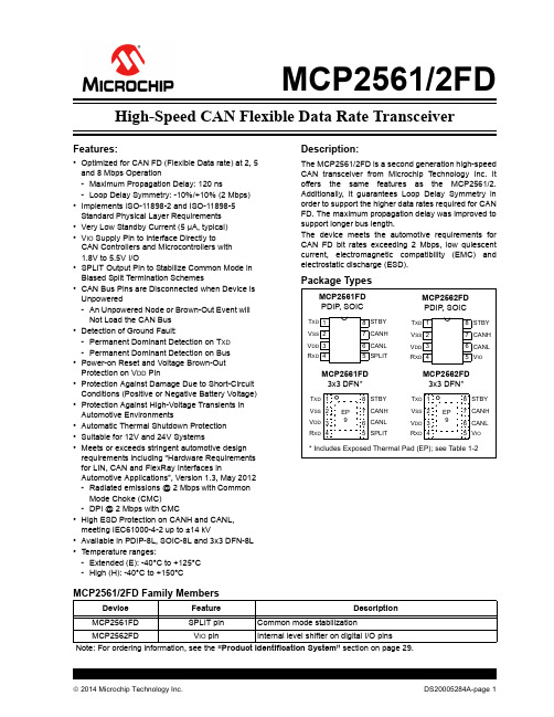
SPLIT(2) VIO(3) VDD
VDD/2
Digital I/O Supply
Thermal Protection
POR UVLO
VIO Permanent Dominant Detect VIO Mode Control Driver and Slope Control CANH
TXD
CANL
STBY
Wake-Up Filter Receiver RXD
CANH
LP_RX(1)
CANL
CANH
HS_RX
CANL
VSS
Note 1: There is only one receiver implemented. The receiver can operate in Low-Power or High-Speed mode. 2: Only MCP2561FD has the SPLIT pin. 3: Only MCP2562FD has the VIO pin. In MCP2561FD, the supply for the digital I/O is internally connected to VDD.
MCP2561/2FD Family Members
Device MCP2561FD MCP2562FD Feature SPLIT pin VIO pin Description Common mode stabilization Internal level shifter on digital I/O pins
Package Types
MCP2561FD PDIP, SOIC
TXD 1 VSS 2 VDD 3 RXD 4 8 STBY 7 CANH 6 CANL 5 SPLIT
MCP601RT中文资料
MCP601/2/3/4
Description
The Microchip Technology Inc. MCP601/2/3/4 family of low-power operational amplifiers (op amps) are offered in single (MCP601), single with Chip Select (CS) (MCP603), dual (MCP602) and quad (MCP604) configurations. These op amps utilize an advanced CMOS technology that provides low bias current, highspeed operation, high open-loop gain and rail-to-rail output swing. This product offering operates with a single supply voltage that can be as low as 2.7V, while drawing 230 µA (typ.) of quiescent current per amplifier. In addition, the common mode input voltage range goes 0.3V below ground, making these amplifiers ideal for single-supply operation. These devices are appropriate for low-power, batteryoperated circuits due to the low quiescent current, for A/D convert driver amplifiers because of their wide bandwidth or for anti-aliasing filters by virtue of their low input bias current. The MCP601, MCP602 and MCP603 are available in standard 8-lead PDIP, SOIC and TSSOP packages. The MCP601 and MCP601R are also available in a standard 5-lead SOT-23 package, while the MCP603 is available in a standard 6-lead SOT-23 package. The MCP604 is offered in standard 14-lead PDIP, SOIC and TSSOP packages. The MCP601/2/3/4 family is available in the Industrial and Extended temperature ranges and has a power supply range of 2.7V to 5.5V.
LTC1605IG资料
1kHz Input Signal, First 5 Harmonics 10kHz Input Signal, First 5 Harmonics
Peak Harmonic or Spurious Noise
1kHz Input Signal 10kHz Input Signal
Full-Power Bandwidth
MIN
TYP
MAX
q 16
q 15
1.0
q
±3
q
±10
±2
±7
q
±0.50
±2
±8
LTC1605A MIN TYP MAX
UNITS
16
Bits
16
Bits
1.0
LSB
±2
LSB
±10
mV
±2
ppm/°C
±5
ppm/°C
±0.25
%
±2
ppm/°C
±8
LSB
2
元器件交易网
VANA = VDIG = VDD
CONDITIONS
(Note 7) Ext. Reference = 2.5V (Note 8)
Ext. Reference = 2.5V (Notes 12, 13) Ext. Reference = 2.5V VDD = 5V ±5% tary Short to VANA Digital Input Voltage (Note 4) ............ VSS – 0.3V to 10V Digital Output Voltage ........ VDGND – 0.3V to VDIG + 0.3V Power Dissipation.............................................. 500mW
MAX16021中文资料
*EP = EXPOSED PAD.
TQFN
Pin Configurations continued at end of data sheet.
________________________________________________________________ Maxim Integrated Products 1
Applications
Main/Backup Power for RTCs, CMOS Memories
Industrial Control
GPS Systems
Set-Top Boxes
Point-of-Sale Equipment
Portable/Battery Equipment
Features
The MAX16016/MAX16020/MAX16021 operate from a 1.53V to 5.5V supply voltage and offer fixed reset thresholds for monitoring 5V, 3.3V, 3V, 2.5V, and 1.8V systems. Each device is available with either a pushpull or open-drain reset output.
RESET, RESET, BATTON ....................................................20mA Continuous Power Dissipation (TA = +70°C)
10-Pin TDFN (derate 24.4mW/°C above +70°C) .......1951mW 16-Pin TQFN (derate 25mW/°C above +70°C) ..........2000mW Thermal Resistance (Note 1) For 10-Pin TDFN θJA ................................................................................41°C/W For 16-Pin TQFN θJA ................................................................................40°C/W Operating Temperature Range ...........................-40°C to +85°C Junction Temperature ......................................................+150°C Storage Temperature Range .............................-65°C to +150°C Lead Temperature (soldering, 10s) .................................+300°C
MEMORY存储芯片TMS320C6416TBGLZ1中文规格书
TMS320C6414, TMS320C6415, TMS320C6416FIXED-POINT DIGITAL SIGNAL PROCESSORSSPRS146N − FEBRUARY 2001 − REVISED MAY 2005 peripheral register descriptions (continued)Table 12. McBSP 1 RegistersHEX ADDRESS RANGE ACRONYM REGISTER NAME COMMENTS0190 0000DRR1McBSP1 data receive register via Configuration Bus The CPU and EDMA controller can only read this register; they cannot write to it.0x3400 0000 − 0x37FF FFFF DRR1McBSP1 data receive register via Peripheral Bus0190 0004DXR1McBSP1 data transmit register via Configuration Bus0x3400 0000 − 0x37FF FFFF DXR1McBSP1 data transmit register via Peripheral Bus0190 0008SPCR1McBSP1 serial port control register0190 000C RCR1McBSP1 receive control register0190 0010XCR1McBSP1 transmit control register0190 0014SRGR1McBSP1 sample rate generator register0190 0018MCR1McBSP1 multichannel control register0190 001C RCERE01McBSP1 enhanced receive channel enable register 00190 0020XCERE01McBSP1 enhanced transmit channel enable register 00190 0024PCR1McBSP1 pin control register0190 0028RCERE11McBSP1 enhanced receive channel enable register 10190 002C XCERE11McBSP1 enhanced transmit channel enable register 10190 0030RCERE21McBSP1 enhanced receive channel enable register 20190 0034XCERE21McBSP1 enhanced transmit channel enable register 20190 0038RCERE31McBSP1 enhanced receive channel enable register 30190 003C XCERE31McBSP1 enhanced transmit channel enable register 30190 0040 − 0193 FFFF–ReservedTable 13. McBSP 2 RegistersHEX ADDRESS RANGE ACRONYM REGISTER NAME COMMENTS01A4 0000DRR2McBSP2 data receive register via Configuration Bus The CPU and EDMA controller can only read this register; they cannot write to it.0x3800 0000 − 0x3BFF FFFF DRR2McBSP2 data receive register via Peripheral Bus 01A4 0004DXR2McBSP2 data transmit register via Configuration Bus 0x3800 0000 − 0x3BFF FFFF DXR2McBSP2 data transmit register via Peripheral Bus 01A4 0008SPCR2McBSP2 serial port control register01A4 000C RCR2McBSP2 receive control register01A4 0010XCR2McBSP2 transmit control register01A4 0014SRGR2McBSP2 sample rate generator register01A4 0018MCR2McBSP2 multichannel control register01A4 001C RCERE02McBSP2 enhanced receive channel enable register 0 01A4 0020XCERE02McBSP2 enhanced transmit channel enable register 0 01A4 0024PCR2McBSP2 pin control register01A4 0028RCERE12McBSP2 enhanced receive channel enable register 1 01A4 002C XCERE12McBSP2 enhanced transmit channel enable register 1 01A4 0030RCERE22McBSP2 enhanced receive channel enable register 2 01A4 0034XCERE22McBSP2 enhanced transmit channel enable register 2 01A4 0038RCERE32McBSP2 enhanced receive channel enable register 3 01A4 003C XCERE32McBSP2 enhanced transmit channel enable register 3 01A4 0040 − 01A7 FFFF–ReservedTMS320C6414, TMS320C6415, TMS320C6416FIXED-POINT DIGITAL SIGNAL PROCESSORSSPRS146N − FEBRUARY 2001 − REVISED MAY 2005peripheral register descriptions (continued)Table 14. Timer 0 RegistersHEX ADDRESS RANGE ACRONYM REGISTER NAME COMMENTS0194 0000CTL0Timer 0 control register Determines the operating mode of the timer, monitors the timer status, and controls the function of the TOUT pin.0194 0004PRD0Timer 0 period register Contains the number of timer input clock cycles to count. This number controls the TSTAT signal frequency.0194 0008CNT0Timer 0 counter register Contains the current value ofthe incrementing counter. 0194 000C − 0197 FFFF−ReservedTable 15. Timer 1 RegistersHEX ADDRESS RANGE ACRONYM REGISTER NAME COMMENTS0198 0000CTL1Timer 1 control register Determines the operating mode of the timer, monitors the timer status, and controls the function of the TOUT pin.0198 0004PRD1Timer 1 period register Contains the number of timer input clock cycles to count. This number controls the TSTAT signal frequency.0198 0008CNT1Timer 1 counter register Contains the current value ofthe incrementing counter. 0198 000C − 019B FFFF−ReservedTable 16. Timer 2 RegistersHEX ADDRESS RANGE ACRONYM REGISTER NAME COMMENTS01AC 0000CTL2Timer 2 control register Determines the operating mode of the timer, monitors the timer status, and controls the function of the TOUT pin.01AC 0004PRD2Timer 2 period register Contains the number of timer input clock cycles to count. This number controls the TSTAT signal frequency.01AC 0008CNT2Timer 2 counter register Contains the current value ofthe incrementing counter. 01AC 000C − 01AF FFFF−Reserved。