RC寄生参数提取在数模混合IC设计中的应用
版图设计中的寄生参数分析
版图设计中的寄生参数分析1.引言正如我们了解的,工艺层是芯片设计的重要组成部分。
一层金属搭在另一层金属上面,一个晶体管靠近另一个晶体管放置,而且这些晶体管全部都是在衬底上制作的。
只要在工艺制造中引入了两种不同的工艺层,就会产生相应的寄生器件,这些寄生器件广泛地分布在芯片各处,更糟糕的是我们无法摆脱它们。
寄生器件是我们非常不希望出现的,它会降低电路的速度,改变频率响应或者一些意想不到的事情发生。
既然寄生是无法避免的,那么电路设计者就要充分将这些因素考虑进去,尽量留一些余量以便把寄生参数带来的影响降至最低。
2.寄生参数的种类寄生参数主要包括了电容寄生、电阻寄生,和电感寄生。
2.1 寄生电容图1所呈现的是在不同金属层之间以及它们与衬底之间产生的电容情况:图(1) 无处不在的寄生电容由上图我们可以看到寄生电容无处不在。
不过需要了解的是即使寄生电容很多,但是如果你的电路设计对电容不十分敏感的时候,我们完全可以忽略它们。
但当电路的设计要求芯片速度很快的时候,或者频率很高时,这些寄生的电容就显得格外重要了。
一般来说,在一个模拟电路中,只要频率超过20MHz 以上,就必须对它们给予注意,否则,它有可能会毁掉你的整个芯片。
减少寄生电容可以从以下几个方面入手:(1)导线长度如果你被告知某个区域的寄生参数要小,最直接有效的方法就是尽量减小导线长度,因为导线长度小的话,与它相互作用而产生的电容例如金属或者衬底层的电容就会相应地减小,这个道理显而易见。
(2)金属层的选择另一种解决的办法则是你的金属层选择。
起主要作用的电容通常是导线与衬底之间的电容,图2则说明了衬底电容对芯片的影响。
Noisy Quiet图(2) 衬底电容产生的噪声影响如上所示,电路1和电路2都对地产生了一个衬底电容,衬底本身又有一个寄生电阻,这样一来电路1的噪声就通过衬底耦合到电路2上面,这是我们不希望看到的。
(设法使所有的噪声都远离衬底)因此我们改变一下金属层,通常情况下,最高金属层所形成的电容总是最小的。
Parasiticextraction:寄生参数提取
OverviewSynopsys’ Star-RCXT™ is the electronic design automation (EDA) industry’s gold standard for parasitic extraction. It provides a single solution for ASIC, system-on-chip (SoC), digital custom,memory and analog designs. Trusted by over 250 semiconductor companies and proven in thousands of production designs, Star-RCXT delivers fast and sub-femtofarad accurate technology. The Star-RCXT solution offers advanced capabilities needed for sub-65-nanometer (nm) designs, including variation-aware parasitic extraction, chemical-mechanical polishing (CMP) based and litho-aware extraction, inductance extraction and analog mixed signal design flow. Its seamless integration with industry leading physical verification, circuit simulation, timing, signal integrity, power, reliability and RTL2GDSII flows enables unmatched ease-of-use, increased productivity and reduced time-to-market. Star-RCXT is used by leading foundries to solve process modeling challenges at 65-nm and 45-nm.Star-RCXT™Parasitic extractionStar-RCXT Parasitic Extraction SolutionSemiconductor process technology has been continually scaling down for the past four decades and the trend continues. In the early days of integrated circuits (ICs), the speed bottleneck was at the circuit level, whereas interconnects were treated as ideal connections with the parasitic effects ignored. With shrinking process technologies, increasing die size and clock frequency, interconnect parasitic effects have begun to manifest themselves in signal delay and noise. Consequently, interconnects now play an important role in the design flow. Today, IC design is interconnect-limited and the design flow is interconnect-driven. A trusted parasitic extraction tool that models advanced process effects and has the capacity to handle large designs with tens of millions of transistors and cells is required to enable designers to quickly achieve their sign-off goals.Star-RCXT has the capacity and accuracy for sign-off extraction on the world’s largest SoC designs. Star-RCXT’s proprietary, advanced technology extracts full-chip designs extremely fast and provides accurate results within 5 percent or 0.2 femto-farad of industry-standard field solvers. Star-RCXT achieves its high accuracy by performing detailed modeling of every capacitive interaction. While, other extraction tools attempt to increase speed by modeling only a subset of the capacitive interactions, Star-RCXT extracts billions of capacitors for a typical design and by using a proprietary parasitic reduction capability, generates the smallest possible netlist, to achieve accurate results. Figure 2 shows excellent correlation between Star-RCXT and Raphael-NXT and demonstrates the accuracy of Star-RCXT.Star-RCXT provides parasitic extraction solution for full-chip gate-level implementation and sign-off as well as for transistor-level custom, memory, analog-mixed-signal (AMS) and radio-frequency (RF) designers, as shown in Figure 1.Gate-level ExtractionStar-RCXT is easily integrated into all industry standard design flows – Synopsys’ Galaxy™ Design Platform, and other third party implementation platforms – using Synopsys’ Milkyway™, LEF/DEF or GDSII interfaces. Galaxy users benefit from the increased productivity of Milkyway as well as the integration and faster convergence and flexibility of full-chip extraction at any time during the design cycle. In addition, Star-RCXT’s tight binary interface with PrimeTime®, PrimeTime SI, PrimeTime PX and integration with PrimeRail enables accurate post-layout optimization and timing, noise and power network sign-off.Transistor-level ExtractionStar-RCXT is integrated with the EDA industry’s leading layout-versus-schematic verification tools and simulation tools – Hercules™, Calibre, HSIM plus, NanoSim™ , HSPICE® and NanoTime for high-seed productive design. Star-RCXT also reads connectivity, cross-reference, and device information from a generated data-base and integrates with third-party analysis tools through industry standard SPICE, DSPF and SPEF netlist formats. For the highest throughput, Star-RCXT offers hierarchical and in-context modes of extraction.Virtuoso Custom Design Platform IntegrationStar-RCXT is integrated with Virtuoso® Analog Design Environment (ADE) for AMS and RF design. Star-RCXT generates Design Framework II (DFII) database parasitic views for netlisting and simulation, compatible with common netlisting interfaces used within ADE. A probing utility is also providedto probe parasitics either within the parasitic view or within the matching schematic view. The parasitic prober also provides the ability to output probed parasitics to an ASCII report file, and to annotate parasitic view total capacitance values to an associated schematic view.Reluctance (Inductance) ExtractionInductance effect becomes more and more prominent as the resistance (both device and interconnect) decreases andthe operating frequency increases. At low frequencies, RC modeling is sufficient and inductance can safely be ignored.As clock frequencies increase, however, modeling global interconnects such as RC circuits are no longer adequate and inductance must be included in the modeling. Ignoring the inductance effect can underestimate signal integrity problems as well.Star-RCXT provides a novel approach to modeling on-chip inductance effects, called partial reluctance extraction. Reluc-tance is defined as the inverse of inductance. Reluctance effects are localized just like capacitance and unlike inductance, resulting in a much sparser matrix compared to inductance. This enables Star-RCXT to produce the smallest netlist without losing any accuracy – overall achieving orders of magnitude faster extraction and simulation.Variation-aware extractionWith shrinking technology, parametric yield due to variationsin critical device and interconnect process parameters has become the dominant factor in yield loss. In order to improve silicon predictability it is mandatory that extraction tools model the process variation accurately. Also, as the uncertainty grows,Figure 1: Star-RCXT provides comprehensive solution for gate-level and transistor-level extractionthe traditional corner-based methodologies requiring multiple process technology files and time-consuming multiple extraction and simulation runs are becoming impractical. Statistical techniques are needed to model these process variation effects. Star-RCXT offers advanced statistical solution that enables sensitivity based parasitic extraction for interconnect process and temperature variation-aware designs at 65-nm and beyond. The variation of each process parameter, such as conductor or dielectric thickness, is available through the variation-aware process technology file and is used to compute sensitivities of parasitic values based on each of the process variations. Star-RCXT’s sensitivity-based extraction solution offers unique benefits to traditional STA flow users as well as to the variation-aware STA flow users, as shown in figure . It enhances the productivity of the traditional flow designers by eliminating the need to do multiple corner extractions, instead providing a single run sensitivity based extraction and multiple netlisting to feed into the traditional analysis – overall, providing 2X faster solution than traditional 5-corner extraction. On the other hand, for variation-aware STA, it generates a single sensitivity-based netlist for fast and robust sign-off. Star-RCXT Key FeaturesComprehensive Process Modeling Conformal dielectric process support Support of Air Gap Via cap extraction Layer ETCHNonlinear RPSQ variation in function of Silicon width Temperature dependent resistance modeling for conducting layers and vias••••••Support of background dielectric Nonlinear via resistance modeling 45-degree routing supportSupport of multiple inter-layer dielectric Support of multiple intra-layer dielectric Support for co-vertical conductors Support for non-planarized metalMultiple cap accuracy mode for different technology (MODE100/MODE200/MODE400) Advanced Process Modeling Sensitivity Extraction CMP simulator interface Litho-aware extractionSingle run multi-corner extraction Reluctance extraction Substrate extractionAccurate D interconnect modelingWidth and Spacing dependent Thickness variation Bottom Thickness variation Density-based thickness variation Multiple density-based variationWidth and Spacing dependent RPSQ variation RPSQ variation in function of Silicon width Nonlinear RPSQ variation Trapezoidal polygon support Dielectric damage modeling Automatic Field Solver FlowCopper interconnect, local interconnect modeling Low-K dielectric, silicon on insulator (SOI) modeling•••••••••••••••••••••••••••Over 99% of nets within 5% or 200aF-10%-5%0%5%10%N u m b e r o f N e t s50100150200250Percentage ErrorFigure 2: Star-RCXT is strongly correlated with Raphael-NXT (field solver)Figure 3: Star-RCXT’s sensitivity based extraction solution supports traditional corner-based and variation-aware STA and simulation flowsGate-level Flow Gray-Box ExtractionDirect interface with Milkyway Database Direct interface with LEF/DEF 5.6Flexibility of Instance port handling Reading of gzip compressed LEF/DEF files Reduction of netlist sizeSupport metal fill polygons from GDSII file.Support GDS inputs for LEF macros.Support hierarchical LEF/DEF inputs.Power net extraction Transistor-level FlowFlexibility of cap threshold handling Resistance threshold handlingAbility to add probe texts to the final netlist Support coupling capacitance to bulk layersSupport all device types including user-defined devices and generic devicesInterface to Hercules physical verificationInterface to Calibre physical verification through CCI Flexibility to control netlist type Support multiple cross-reference flowFlexibility of ignoring the parameter parasitic presented in spice modelSupport parasitic with model namesAbility to extract device of shrunk design parasitic for actual drawn design••••••••••••••••••••••Productivity and Ease of Use Incremental Extraction Distributed Processing License Queuing ADE integration Hierarchical Extraction Selective net extractionSupport of multiple netlist formats (SBPF/SPF/SPEF) Ability to control a number of characters in a line of netlist Ability to write device parameter in parasitic netlist Ability to split power net parasitic into a separate netlist Ability to extract device parameters such as width/length and report in parasitic netlistAbility to output original design coordinates of instance.Ability to extract a design in a given temperature Ability to read time capacitance or designed cap during extractionAbility to extract multiple corners simultaneously Ability to merge multiple extraction result to one file Flexibility to control of ground capacitanceAbility to write parasitic diode to parasitic capacitance User-control reduction of parasitic netlists Multiple reduction mode for different application Validated silicon models available from leading foundries including TSMC, UMC, Chartered•••••••••••••••••••••Synopsys, Inc.700 East Middlefield Road Mountain View, CA 9404 Specifications File Format SupportStar-RCXT supports the following industry-standard formats and interfaces:Layout data in: GDSII, LEF/DEF, Milkyway, Hercules,CalibreOutput formats: DSPF, SPICE, SPEF, SSPEF Binary interface: Direct binary interface to PrimeTime SI System RequirementsDRAM: 512MB, recommend 1GB Swap Space: 512MB, recommend 2GBInstallation disk space: 250MB baseline plus 250MB per platformDesign disk space depends on the circuit size, recommended minimum 500MB•••••••For more information about this product, sales, support services or training, please contact your local Synopsys representative or call 1-800-388-9125.。
CalibrexRC的使用

CalibrexRC的使⽤Calibre xRC 的使⽤1.版图中的寄⽣参数在使⽤Calibre xRC提取寄⽣参数之前,先介绍⼀下电路中的寄⽣参数。
⼀般来讲,寄⽣参数有寄⽣电阻、寄⽣电容、寄⽣电感等,其中寄⽣电阻和寄⽣电容对电路的影响最为明显。
在版图中,各导电层如铝线、多晶等及导电层之间的接触孔只要有电流通过就会有寄⽣电阻。
两层导电层之间会存在寄⽣电容,寄⽣电容⼀般可分为本征(intrinsic)和耦合(coupled)两种,本征电容是指导电层到衬底(substrate)的电容,它有两种类型,如图1中所⽰:#1为intrinsic plate电容,#4和#5为intrinsic fringe电容;耦合电容是指导电层在不同⽹线之间的电容,图1中#2、#3和#6就属于这种,其中#2为nearbody 电容,#3为crossover fringe电容,#6为crossover plate电容。
图1 寄⽣电容模型电路中寄⽣参数的存在给电路的⼯作造成了⼀定的影响,寄⽣电阻的存在会影响到电路的功耗,寄⽣RC会影响电路中的信号完整性,等等。
所以在版图完成后,必须提取出版图中的寄⽣参数,将它们反标⼊逻辑电路中⼀起进⾏仿真,以此来检查版图设计的准确性。
2.Calibre xRC功能简介Calibre xRC提供了多种寄⽣参数提取解决⽅案。
它可以根据电路设计的不同要求来提取不同的寄⽣参数⽹表,针对全定制电路和模拟电路可以提取晶体管级(transistor level)的⽹表,针对⾃动布局布线产⽣的电路可以提取门级(gate level)⽹表,针对数模混合电路可以提取混合级(ADMS)的电路⽹表。
它还可以根据不同的电路分析要求进⾏提取,针对电路的功耗(Power)分析,只进⾏寄⽣电阻的提取,针对电路的噪声(Noise)分析⽽仅对寄⽣电容的提取,针对电路的时序(Timing)分析⽽提取相应的RC或RCC⽹表,针对电路的信号完整性(Signal Integrity)分析提取寄⽣RC或RCC⽹表。
RC寄生参数提取在数模混合IC设计中的应用
1概述基于全定制设计方法设计的模拟模块以及标准单元库在完成版图工作后,为确保版图符合设计要求且连线正确需要进行DRC和LVS检查。
集成电路通过版图设计最终转化到硅片后,由于同层以及不同层材料之间寄生参数的影响会使电路性能与最初仿真结果产生偏差甚至使电路无法正常工作。
因此,电路完成DRC和LVS后还需进行版图寄生参数提取(LPE:layout parasitic extraction)和寄生电阻提取(PRE,parasitic resistance extraction)[1]。
大规模数字集成电路芯片的物理实施中,完成布线后的一项重要工作是进行静态时序分析(STA:static timing analysis)。
在时序分析前,则首先需要对芯片的物理版图设计进行包括电阻、电容以及电感的参数提取,再进行延时计算。
版图设计的完整寄生参数应当包括R、C、L、K,其中L(电感)和K(互感)在单元库版图和低频数字IC中常常忽略[2]。
LPE/PRE完成后我们将会得到一个含有大量寄生元件信息的电路SPICE或CDL 格式网表文件。
该网表文件反映了电路版图的精确特性。
用它进行SPICE后仿真(post-simulation)。
如RC寄生参数提取在数模混合IC设计中的应用王巍(国家集成电路设计深圳产业化基地)摘要:目前的数模混合集成电路设计中,需要对模拟部分进行后版图仿真并对整体电路进行时序分析。
版图后仿真需要进行晶体管级的寄生参数提取,芯片时序分析则需要对互连线进行寄生参数提取。
RC 寄生参数提取的精确度和效率在很大程度上影响着整体芯片设计的质量和效率。
Abstract:In the current mixed analog-digital circuit design,the analog module need to do post-layout simulation and the full-chip need to do STA.While the post-layout simulation need the RC extraction in transistor-level and the interconnect delay also need to be extracted in order to do STA.The definition and efficiency of the RC extraction are very important to the quality of the full-chip design.果后仿真结果同样满足设计要求,那么这时就能够确定版图设计有问题。
使用Calibre实现RFCMOS电路寄生参量的提取及后仿真

使⽤Calibre实现RFCMOS电路寄⽣参量的提取及后仿真使⽤Calibre xRC实现RFCMOS电路的寄⽣参量提取及后仿真郭慧民[摘要]Calibre xRC是Mentor Graphics公司⽤于寄⽣参量提取的⼯具,其强⼤的功能和良好的易⽤性使其得到业界的⼴泛认可。
本⽂以采⽤RFCMOS⼯艺实现的LNA为例,介绍使⽤Calibre xRC对RFCMOS电路寄⽣参量提取,以Calibreview 形式输出以及在Virtuoso的ADE中直接后仿真的流程。
本⽂还将讨论Calibre xRC特有的XCELL⽅式对包含RF器件的电路仿真结果的影响。
采⽤Calibre xRC提取寄⽣参量采⽤RFCMOS⼯艺设计低噪声放⼤器(LNA),其电路图如图1所⽰,版图如图2所⽰。
图1 LNA的电路图图2 LNA的版图Calibre⽀持将其快捷⽅式嵌⼊在Virtuoso平台中。
⽤户只需在⾃⼰.cdsinit⽂件中加⼊以下⼀⾏语句:load( strcat( getShellEnvVar("MGC_HOME") "/lib/calibre.skl" ))就可以在virtuoso的菜单中出现“calibre”⼀项,包含如下菜单:点击Run PEX,启动Calibre xRC的GUI,如图3所⽰。
Outputs菜单中的Extraction Type⾥,第⼀项通常选择Transistor Level 或Gate Level,分别代表晶体管级提取和门级提取。
第⼆项可以选择R+C+CC,R+C,R,C+CC,其中R 代表寄⽣电阻,C 代表本征寄⽣电容,CC代表耦合电容。
第三项可以选择No Inductance,L或L+M,分别代表不提取电感,只提取⾃感和提取⾃感与互感。
这些设置由电路图的规模和提取的精度⽽定。
在Format⼀栏中,可以选择SPECTRE,ELDO,HSPICE等⽹表形式,也可以选择Calibre xRC提供的CALIBREVIEW形式。
【经验】以一个例子分析有源滤波器中元件的寄生参数的影响

【经验】以一个例子分析有源滤波器中元件的寄生参数的影响下图是一个有源带通滤波器。
理论分析的结果是:当图中所有相同标号的元件取相同数值的话,其中心频率为1/(2*pi*RC),Q值为R1/R,中心频率的电压增益为2倍。
由于这个电路的中心频率与Q值相互独立,且Q值仅与两个电阻之比值有关,所以可以用在需要高Q 值的电路中。
然而在实际应用中,很多时候这个电路的表现却是差强人意,主要的问题是Q值不容易做高。
原因何在?这个电路可以等效成下图所示的 LC谐振回路。
两个运放以及排成一列的RC等效为一个电感,其阻抗表达式是Z=jw(R^2)C,由于在中心频率上w0=1/(RC),所以Z0=jR。
下面讨论这个电路的Q值。
为了说明方便,将前面的图改画成如下形式:在前面的计算中,并没有考虑上图中的RL,所以就得到Q=R1/XL=R1/R(XL是那个等效电感在中心频率上的电抗)。
但是在实际电路中由于寄生参数的影响,在这个LC并联回路两端存在一个损耗电阻RL,由于这个电阻的存在,整个电路的Q值将下降到Q=(R1||RL)/R。
现在的问题就是:如何估计这个RL?一个似乎很显见的影响是运放的输入电阻。
但是在有源滤波器中,电阻值通常在千欧姆数量级,而运放的输入电阻常常高于百兆欧姆,所以实际上运放的输入电阻对于Q值的影响可以忽略。
事实上,对这个电路影响最大的是电容C的Q值。
较少有人关注电容的Q值,一种错误的看法是电容的漏电极小所以一定有很高的Q值。
但实际上电容的Q值并没有想象的那么高。
在低频范围内工作的有源滤波器,其中的电容常常采用薄膜电容。
薄膜电容器是用金属箔电极与塑料薄膜卷绕而成,为了减小体积,现在大部分薄膜电容中的电极都是在塑料薄膜上蒸镀的一层金属层。
由于蒸镀的金属层很薄所以有较大的寄生电阻(ESR),又由于卷绕形成了寄生电感,所以这些电容往往在低频的时候有很好的性能,但是频率稍高就表现出损耗加大、容量下降等现象。
笔者曾经用电桥测量过多个薄膜电容,在几百赫兹频率下都表现良好,但是当频率加大到几十千赫兹后大部分电容都出现了容量下降,Q值下降的现象。
IC设计流程之实现篇——全定制设计

IC设计流程之实现篇——全定制设计要谈IC设计的流程,⾸先得搞清楚IC和IC设计的分类。
集成电路芯⽚从⽤途上可以分为两⼤类:通⽤IC(如CPU、DRAM/SRAM、接⼝芯⽚等)和专⽤IC(ASIC)(Application Specific Integrated Circuit),ASIC是特定⽤途的IC。
从结构上可以分为数字IC、模拟IC和数模混合IC三种,⽽SOC(System On Chip,从属于数模混合IC)则会成为IC设计的主流。
从实现⽅法上IC设计⼜可以分为三种,全定制(full custom)、半定制(Semi-custom)和基于可编程器件的IC设计。
全定制设计⽅法是指基于晶体管级,所有器件和互连版图都⽤⼿⼯⽣成的设计⽅法,这种⽅法⽐较适合⼤批量⽣产、要求集成度⾼、速度快、⾯积⼩、功耗低的通⽤IC或ASIC。
基于门阵列(gate-array)和标准单元(standard-cell)的半定制设计由于其成本低、周期短、芯⽚利⽤率低⽽适合于⼩批量、速度快的芯⽚。
最后⼀种IC 设计⽅向,则是基于PLD或FPGA器件的IC设计模式,是⼀种“快速原型设计”,因其易⽤性和可编程性受到对IC制造⼯艺不甚熟悉的系统集成⽤户的欢迎,最⼤的特点就是只需懂得硬件描述语⾔就可以使⽤EDA⼯具写⼊芯⽚功能。
从采⽤的⼯艺可以分成双极型(bipolar),MOS和其他的特殊⼯艺。
硅(Si)基半导体⼯艺中的双极型器件由于功耗⼤、集成度相对低,在近年随亚微⽶深亚微⽶⼯艺的的迅速发展,在速度上对MOS管已不具优势,因⽽很快被集成度⾼,功耗低、抗⼲扰能⼒强的MOS管所替代。
MOSFET⼯艺⼜可分为NMOS、PMOS和CMOS三种;其中CMOS⼯艺发展已经⼗分成熟,占据IC市场的绝⼤部分份额。
GaAs器件因为其在⾼频领域(可以在0.35um下很轻松作到10GHz)如微波IC中的⼴泛应⽤,其特殊的⼯艺也得到了深⼊研究。
⽽应⽤于视频采集领域的CCD传感器虽然也使⽤IC⼀样的平⾯⼯艺,但其实现和标准半导体⼯艺有很⼤不同。
数模混合IC设计流程
数模混合IC设计流程1.数模混合IC设计近十年来,随着深亚微米及纳米技术的发展,促使芯片设计与制造由分离IC、ASIC 向SoC转变,现在SoC芯片也由数字SoC全面转向混合SoC,成为真正意义上的系统级芯片。
如今人们可以在一块芯片上集成数亿只晶体管和多种类型的电路结构。
此时芯片的制造工艺已经超越了传统制造理论的界限,对电路的物理实现具有不可忽略的影响。
因此,片上系统所依赖的半导体物理实现方式,面临着多样化和复杂化的趋势,设计周期也越来越长。
目前越来越多的设计正向混合信号发展。
最近,IBS Corp做过的一个研究预测,到2006年,所有的集成电路设计中,有73%将为混合信号设计。
目前混合信号技术正是EDA业内最为热门的话题。
设计师在最近才开始注意到混合信号设计并严肃对待,在他们意识到这一领域成为热点之前,EDA公司已经先行多年。
EDA业内领头的三大供应商Mentor Graphics、Synopsys和Cadence在几年前即开始合并或研发模拟和混合信号工具和技术。
其中Mentor Graphics是第一个意识到这一点,并投入力量发展混合信号技术的EDA供应商。
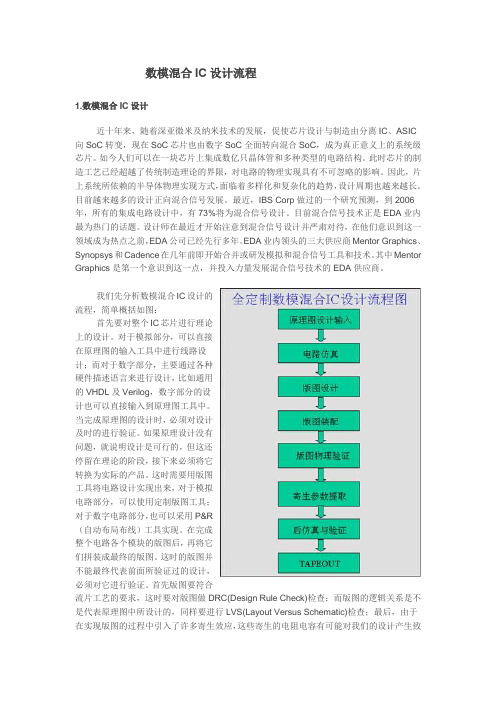
我们先分析数模混合IC设计的流程,简单概括如图:首先要对整个IC芯片进行理论上的设计。
对于模拟部分,可以直接在原理图的输入工具中进行线路设计;而对于数字部分,主要通过各种硬件描述语言来进行设计,比如通用的VHDL及Verilog,数字部分的设计也可以直接输入到原理图工具中。
当完成原理图的设计时,必须对设计及时的进行验证。
如果原理设计没有问题,就说明设计是可行的,但这还停留在理论的阶段,接下来必须将它转换为实际的产品。
这时需要用版图工具将电路设计实现出来,对于模拟电路部分,可以使用定制版图工具;对于数字电路部分,也可以采用P&R(自动布局布线)工具实现。
在完成整个电路各个模块的版图后,再将它们拼装成最终的版图。
这时的版图并不能最终代表前面所验证过的设计,必须对它进行验证。
- 1、下载文档前请自行甄别文档内容的完整性,平台不提供额外的编辑、内容补充、找答案等附加服务。
- 2、"仅部分预览"的文档,不可在线预览部分如存在完整性等问题,可反馈申请退款(可完整预览的文档不适用该条件!)。
- 3、如文档侵犯您的权益,请联系客服反馈,我们会尽快为您处理(人工客服工作时间:9:00-18:30)。
RC寄生参数提取在数模混合IC设计中的应用数模混合IC设计是一个广泛应用于现代集成电路设计中的技术。
它将数字电路和模拟电路集成在一起,可以实现更高的功耗效率和更好的性能。
在数模混合IC设计中,RC寄生参数提取扮演了重要的角色。
RC寄生参数是指电路布线过程中由于电阻和电容元件之间的信号传输造成的非理想情况。
这些寄生参数可以导致信号的失真、串扰和延迟等问题。
因此,精确提取和建模这些寄生参数对于确保电路性能的准确性和稳定性是至关重要的。
在数模混合IC设计中,RC寄生参数提取有以下几个主要的应用:
1.电路仿真:在电路设计的早期阶段,设计师需要通过仿真来评估电路的性能。
然而,由于RC寄生参数的存在,仿真结果可能与实际情况有所偏差。
因此,在仿真之前,需要进行RC寄生参数的提取和建模,以保证仿真结果的准确性。
2.时序分析:在数模混合IC设计中,时序分析是一个非常重要的步骤。
它用于评估电路的时钟频率、传输延迟和电路的可靠性等。
然而,由于RC寄生参数的存在,时序分析可能会遇到一些挑战。
因此,需要准确提取和建模RC寄生参数,以便进行准确的时序分析。
3.信号完整性分析:在高速电路设计中,信号完整性是一个重要的问题。
由于RC寄生参数的存在,电路中的信号传输可能遇到失真、串扰和延迟等问题,从而导致信号完整性下降。
因此,在进行信号完整性分析之前,需要准确提取和建模RC寄生参数,以评估信号的完整性。
4.线长匹配:在数模混合IC设计中,线长匹配对于电路的稳定性和性能至关重要。
由于RC寄生参数的影响,不同信号线的传输延迟可能存
在差异。
因此,在布线过程中,需要准确提取和建模RC寄生参数,以确保不同信号线的传输延迟保持匹配,从而提高电路的性能。
综上所述,RC寄生参数提取在数模混合IC设计中具有重要的应用价值。
它能够准确提取和建模电路中的寄生参数,从而保证电路性能的准确性和稳定性。
通过RC寄生参数提取,可以实现更精确的电路仿真、时序分析、信号完整性分析和线长匹配,从而提高整个数模混合IC设计的效率和可靠性。