CH11-电路宏模型06071
TCL王牌LE32D8810液晶彩电图纸

N/A N/A N/A 有 N/A N/A 1 1 1 1 2 1 1 0 0 0 0 1 0 0 1 否 一体 750*200*515 750.3x73*466.5 886*132*580 5.3 KG
6.5KG 8.7KG
200*100 M4 宽电压
100-240V 50Hz 70W
小于 0.5W 1级 1.7 N/A N/A 100 N/A
响应时间
灰度级
色温
色域
声音
2D 可视角(CR>10:1) 3D 可视角(Crosstalk<3%) 声音制式
声音模式
内置扬声器个数
喇叭规格
伴音输出功率
重低音
32" LE32C12 LE32D8810
MTC AU/SHARP/BOE
A 1366*768 MSTAR 6M182 左右上 24.91,下 39.65
4、使用者的警告 4.1 警告:
为了防止电击或火灾,请不要将电视放到有雨雾的场所。不要使用任何可能对显示屏造成刮 伤、毁坏的硬物体磨擦或敲击显示屏。 4.2 注意: 禁止在未经授权的情况下以任何方式私自更改本产品。 4.3 供电电源 产品直接用交流电供电,供电电压值见电视后盖标牌上的说明。将交流电源线一端按照电视 后端子标牌标注位置插入电源端口,另一端接在电源插座即可完成电源连接。 在有雷电或交 流供电断电的时候,请拔掉电源插头和天线插头。电源线不允许有任何其它东西帖靠或缠绕 在上面,也不要将电源线置于可能受到毁坏的地方。 4.4 使用场所 避免电视的屏幕直接对着外界的强光或阳光。避免电视受到不必要的任何振动,不要将电视 置于过湿、过热或多灰尘的地方。保证电视有良好的空气对流,不要将任何物体覆盖在后盖 的通风口上。 4.5 清洁 在清洁电视屏之前将电源插头拔下。使用干净的软布擦拭显示屏和电源线。如果显示屏需要 特别的清洗,请使用干净、潮湿的抹布进行擦拭。请不要使用任何汽油、酒精、苯类有机液 体或气雾状清洁剂。请不要用力过大以致损坏屏幕。 4.6 注意事项 显示屏属于精密显示器件,屏幕上有个别的亮点、暗点,或红、绿、蓝色之类的少许死像素 这是正常现象,不属于不良品。 A、显示屏长时间显示同一个静止画面时,会在电视上留下一 个残影,这种损坏属于使用不当造成的。 B、电视在连接各种系统时,可能会出现系统不匹 配的现象,特别是连接电脑时,有些显卡可能不匹配,而且本机只识别刷新率为 60HZ。 C、 由于本机使用嵌入式的操作系统,软件比较复杂,可能在工作中或待机中出现软件问题,如 果重新启动能恢复正常,就不属于故障。
DSC-CN5711

最大结温…………………...150℃ 存储温度…………………....-65℃ to 150℃ 焊接温度…………………...260℃
超出以上所列的极限参数可能造成器件的永久损坏。以上给出的仅仅是极限范围,在这样的极限条件下 工作,器件的技术指标将得不到保证,长期在这种条件下还会影响器件的可靠性。
输入电源
3
4
8
VCC VCC
CE
5 LED LED 6
CN5711
可调 电阻
RISET2
RISET1
1 ISET
GND 2
图5 用可变电阻调整发光二极管的亮度
6
REV 1.1
如韵电子 CONSONANCE
稳定性
通常情况下,在ISET管脚没有外加电容时,在此管脚可以接一个阻值最大为30K的电阻。如果在ISET管 脚有外接的电容,则在此管脚允许外接的电阻值会减小。为了保证电流回路的稳定性,ISET管脚外接电 阻,电容所形成的极点应高于300KHz。假设ISET管脚外接电容C,用下面的公式可以计算ISET管脚允许 外接的最大电阻值:
REV 1.1
如韵电子 CONSONANCE
典型应用电路:
图 1 典型应用电路
订购信息:
器件型号 CN5711
封装形式 SOP8
包装 盘装,每盘 2500 只
工作环境温度 -40℃ 到 85℃
功能框图:
CE ISET
Sc hmitt
VCC
+
电压基准源
电流镜
GND
图 2 功能框图
2
LED
REV 1.1
如韵电子 CONSONANCE
管脚描述:
序号.
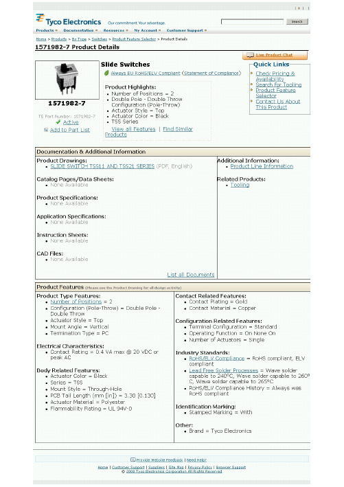
1571982-7资料
矿产资源开发利用方案编写内容要求及审查大纲
矿产资源开发利用方案编写内容要求及《矿产资源开发利用方案》审查大纲一、概述
㈠矿区位置、隶属关系和企业性质。
如为改扩建矿山, 应说明矿山现状、
特点及存在的主要问题。
㈡编制依据
(1简述项目前期工作进展情况及与有关方面对项目的意向性协议情况。
(2 列出开发利用方案编制所依据的主要基础性资料的名称。
如经储量管理部门认定的矿区地质勘探报告、选矿试验报告、加工利用试验报告、工程地质初评资料、矿区水文资料和供水资料等。
对改、扩建矿山应有生产实际资料, 如矿山总平面现状图、矿床开拓系统图、采场现状图和主要采选设备清单等。
二、矿产品需求现状和预测
㈠该矿产在国内需求情况和市场供应情况
1、矿产品现状及加工利用趋向。
2、国内近、远期的需求量及主要销向预测。
㈡产品价格分析
1、国内矿产品价格现状。
2、矿产品价格稳定性及变化趋势。
三、矿产资源概况
㈠矿区总体概况
1、矿区总体规划情况。
2、矿区矿产资源概况。
3、该设计与矿区总体开发的关系。
㈡该设计项目的资源概况
1、矿床地质及构造特征。
2、矿床开采技术条件及水文地质条件。
SDS9-6CNCH1D数控系统规格说明书20111216
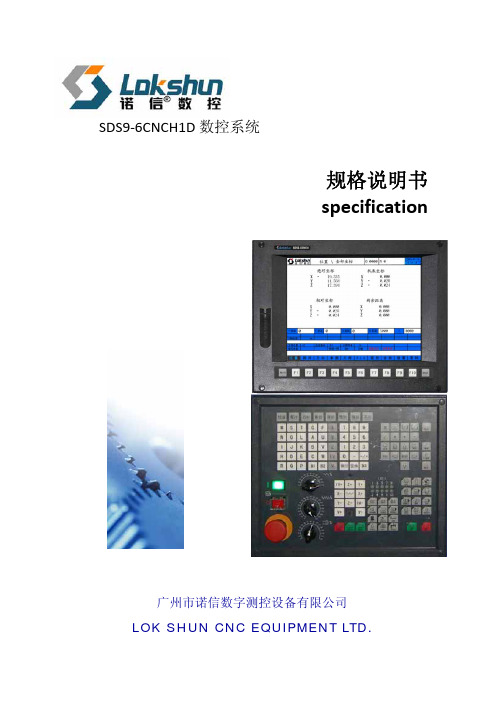
规格说明书 specification
广州市诺信数字测控设备有限公司 LOK SHUN CNC EQUIPMENT LTD.
广州市诺信数字测控设备有限公司
系统简介
SDS9‐6CNCH1D 数控系统以 32 位微处理嵌入式 芯片作为系统主控模块的核心,其功能强大、内置 资源丰富,配以 1024x768 分辨率的液晶彩屏用于 用户加工交互操作显示;以高精度浮点 DSP 和 CPLD 作为加工插补模块的核心;综合运用了实时嵌入式 系统技术、DSP 技术、CPLD 技术、高速高精度光栅 尺测量技术、以太网传输技术等。本产品可配套雕 刻机、雕铣机,主要应用于中端数控机床市场。
第 1 位:(信号类型)
符号
规格
A
脉冲型
第 2 位:(液晶屏)
符号
规格
C
12.1 寸彩色液晶屏
第 3 位:(按键键盘类型)
符号
规格
B
通用编辑功能一体化键盘
第 4 位:(I/O 控制盒类型)
符号
规格
B
支持 36 路输入,36 路输出接口
第 5 位:(系统箱类型)
符号
规格
0
不带控制器箱体
A
LokShun(9-6CNCH)控制器箱体
自动对刀仪
自动对刀长度补偿
△
自动对刀半径补偿
△
语言
中文
○
英文
○
插补周期(ms)
0.5ms(最小)
轨迹前瞻(条)
100
高速断点
条号断点和刀号断点
○(5000 条/s)
2
广州市诺信数字测控设备有限公司
目录文件管理系统 子程序调用 宏程序调用 单节功能 程序预演功能 程序 MDI 功能 程序手工编辑功能 暂停功能 孔加工循环 主轴任意点定位 刀具补偿
HA16107FP资料

Vref UVL2
UVL1 ST
+ + − PWM Comparator
Triangle waveform
UVL1 and UVL2 Pulse-by-pulse latch
Triangle waveform OSC
QCLM
QR QS
OUT
VC
VE
Vref
Current limiter
6
HA16107P/FP, HA16108P/FP
1. Timing in Normal Operation
Timing in these ICs is based on a triangular voltage waveform. The rising edge (leading edge) defines the deadband time tDB. The falling edge (trailing edge) defines the ON-duty control band tON. PWM output is on in the area within tON that is bounded above by the triangle wave VCT and error output VE/O. The following pin outputs are related to PWM control:
Ordering Information
Product HA16107P HA16107FP HA16108P HA16108FP
Typical Threshold Voltage
UVL1
OVP
Hi: 16.2 V
7.0 V
Lo: 9.5 V
SIM6800M系列应用手册

1 4"/,&/&-&$53*$$0 -5%
7FS
)JHI7PMUBHFQIBTF.PUPS%SJWFS*$ 4*..4FSJFT
"QQMJDBUJPO /PUF
1.产品概要 SIM6800M 系列是将输出功率器件具有各种保护功能的预驱 IC、带有限流电阻的自举二极管封装在一起的逆 变ɾ功率ɾ模块。 适用于风扇、泵、压缩机等高压 相电机逆变应用。 图 1 所示为内部方块图。
7FS
)JHI7PMUBHFQIBTF.PUPS%SJWFS*$ 4*..4FSJFT
"QQMJDBUJPO/PUF
SIM6800M 系列 应用手册
目录 1 . 产 品 概 要 . . . . . . . . . . . . . . . . . . . . . . . . . . . . . . . . . . . . . . . 2 2 . 特 征 . . . . . . . . . . . . . . . . . . . . . . . . . . . . . . . . . . . . . . . . . . 3 3 . 产 品 一 览 . . . . . . . . . . . . . . . . . . . . . . . . . . . . . . . . . . . . . . . 5 4 . 端 子 功 能 . . . . . . . . . . . . . . . . . . . . . . . . . . . . . . . . . . . . . . . 6 5 . 保 护 功 能 . . . . . . . . . . . . . . . . . . . . . . . . . . . . . . . . . . . . . . . 1 1 6 . 应 用 电 路 例 . . . . . . . . . . . . . . . . . . . . . . . . . . . . . . . . . . . . . 1 6 7 . 使 用 上 的 注 意 点 . . . . . . . . . . . . . . . . . . . . . . . . . . . . . . . . . 1 9 8. 特性数据
SGM3001中文资料
Operating Temperature Range...........................- 40°C to +125°C Junction Temperature...........................................................+150°C Storage Temperature.............................................- 65°C to +150°C Lead Temperature (soldering, 10s).......................................260°C ESD Susceptibility HBM..........................................................................................2000V MM..............................................................................................400V
3001 SGM3002XMS
PACKAGE OPTION
Tape and Reel, 3000 Tape and Reel, 3000
ABSOLUTE MAXIMUM RATINGS
V+ to GND....................................................................- 0.3V to +6V
Channel ON Leakage current DIGITAL INPUTS Input High Voltage Input Low Voltage
Concept常见问题
1.关于编程软件ConceptXS , ConceptS , ConceptM , ConceptXL主要区别。
ConceptXS和ConceptS 只能对Momentum PLC 进行编程, 无Concept Security。
ConceptM可对Compact 和Momentum PLC进行编程,无Concept Security。
ConceptXL可对Quantum、Compact、Momentum、Atrium进行编程,有Concept Security。
2.Concept S 和Concept M有多用户版吗?对于Concept软件而言, 只有XL版才有单用户和多用户版, 而Concept S 和Concept M 只有单用户版, 没有多用户版, 所以如果用户需要3个Concept M的拷贝的话, 那么用户必须定3套Concept M的单用户版.3. Quantum以太网模板140NOE771X0上Appl灯亮,是什么原因?怎样使之熄灭?NOE模板如果发生过系统崩溃,就会在模板内部创建一个记录文件,并且NOE模板上的Appl灯亮。
要想使之熄灭,用IE浏览器进入NOE模板,进入NOE Diagnostics,再进入Crash Log File Diagnostics,崩溃信息会显示出来,点击“Clear Crash Log File”,就可以清除这些崩溃信息,Appl灯也会熄灭。
4.在Concept2.2 SR2做I/O map时,找不到Quantum As-i模板140EIA92100,此模板有可能应用于Concept2.2 SR2下吗?Quantum As-i模板能配置在本地机架,RIO分站,DIO分站上吗?Concept2.2 SR2不支持As-i模板140EIA92100,必须是Concept v2.5,Modsoft v2.61,Proworx Nxt v2.1支持此模板。
此模板可配置在本地机架,RIO分站,DIO分站上。
OB2211, OB2212 Datasheet
GENERAL DESCRIPTIONOB2211/OB2212 series is an offline PWM Power switch for low power AC/DC charger and adaptor applications. It operates in primary-side sensing and regulation, thus, opto-coupler and TL431 is eliminated. It achieves excellent Constant Voltage (CV) and Constant Current (CC) performance by built-in constant current and constant voltage control, as shown in the figure below. OB2211/OB2212 operates with flyback converter in DCM mode. The pulse frequency modulation (PFM) is used in CC control. In CV control, multi-mode operations are utilized to achieve high performance and efficiency: fixed frequency mode at large load conditions; frequency reduction mode atlight/medium load; ‘Extended burst mode’ atNo/light load. OB2211/OB2212 offers complete protection coverage with auto-recovery features including Cycle-by-Cycle current limiting, VDD over-voltage clamp and UVLO, and Power on soft start. Excellent EMI performance is achieved with On-Bright proprietary frequency shuffling technique together with soft switching control at the totem pole gate FEATURESPrimary-side Sensing and Regulation WithoutTL431 and Opto-couplerMulti-mode Operation for High Efficiency Programmable CV and CC RegulationFrequency Shuffling and Adjustable Gate Drive Greatly Improving EMIPower on Soft-start Time (4ms)“Extended Burst Mode Control” for Improved Efficiency and Minimum Standby Design Built-in Leading Edge Blanking Cycle-by-Cycle Current LimitingVDD Under Voltage Lockout with Hysteresis (UVLO)Gate Output Maximum Voltage Clamp (16V) Auto-restart in Short Circuit APPLICATIONSLow Power AC/DC offline SMPS for Cell Phone ChargerDigital Cameras Charger Small Power AdaptorAuxiliary Power for PC, TV etc. Linear Regulator/RCC Replacement OB2211 is offered in SOP8 package.OB2212 is offered in DIP8 packageTYPICAL APPLICATIONGENERAL INFORMATION Pin ConfigurationOB2211 is offered in SOP8OB2212 is offered in DIP8The pin map is shown as below.Ordering InformationPart Number DescriptionOB2211CP SOP8,Pb-freeOB2211CPA SOP8, Pb-free, T&ROB2212AP DIP8,Pb-freeNote: All Devices are offered in Pb-free Package if not otherwisenoted.Package Dissipation RatingPackage RθJA (°C/W)SOP8 150DIP8 90Absolute Maximum RatingsParameter ValueDrain Voltage (off state)-0.3V to 650VVDD Voltage -0.3 to 38 VVDDG Voltage -0.3 to 38 VVDD Zener Clamp ContinuousCurrent10 mACS Input Voltage-0.3 to 7VINV Input Voltage-0.3 to 7VMin/Max Operating JunctionTemperature T J-20 to 150 o CMin/Max Storage TemperatureT stg-55 to 150 oCLead Temperature (Soldering,10secs)260 oCNote: Stresses beyond those listed under “absolute maximumratings” may cause permanent damage to the device. These arestress ratings only, functional operation of the device at these orany other conditions beyond those indicated under “recommendedoperating conditions” is not implied. Exposure to absolutemaximum-rated conditions for extended periods may affect devicereliability.Marking InformationTERMINAL ASSIGNMENTSPin Num Pin Name I/O Description1 VDDG P Internal Gate Driver Power Supply2 VDD P IC DC power supply Input3 INV I Inverting input of error amplifier (EA). Connected to resistor divider fromprimary sensing winding reflecting output voltage. PWM duty cycle isdetermined by EA output and current sense signal at pin 4.4 CS I Current sense input5/6 Drain O HV MOSFET Drain Pin. The Drain pin is connected to the primary lead ofthe transformerGround8 GND POutput Power Table230VAC±15% 90-264VAC ProductOpen Frame1 Open Frame1OB2211 10W 8WOB2212 20W 12W Notes:1. Maximum practical continuous power in an open frame design with sufficient drain pattern as a heat sink, at 50℃ ambient.BLOCK DIAGRAMRECOMMENDED OPERATING CONDITIONSymbol Parameter Min Max UnitVoltage 12 23 V VDD VDDSupplyT A Operating Ambient Temperature -20 85 o CELECTRICAL CHARACTERISTICS(T A = 25O C , VDD=VDDG=16V, if not otherwise noted)Symbol Parameter Test Conditions Min Typ Max Unit Supply Voltage (VDD) Section I DD ST Standby current Start up current, VDD=13V 5 10 uAI DD op Operation Current Operation supply current INV=1.25V, CS=0V, VDD=VDDG=20V- 1.02.0 mA UVLO(ON) VDD Under Voltage Lockout Enter7.5 8.5 10.0 VUVLO(OFF) VDD Under Voltage Lockout Out13.5 14.7 16.0 VV DD _clamp I DD =10mA 38 V Current Sense Input SectionT LEB LEB time 540 ns Vth_oc V TH _OC_test800 830 860 mV Td_oc Propagation delay 150 ns Z SENSE _IN Input Impedance 50 Kohm T_ss Soft start time 4 ms Oscillator Section (CV) Fosc normal mode frequency48 50 52 KHz Fosc_Burst Green-Mode min.Frequency22 KHz△f/FoscFrequency shuffling range+/-4 % CC Section VDD=16V VDDG=16V INV=0V (minimum frequen 12.2 KHz VDD=16V VDDG=16V INV=0.35V 14.7 KHz VDD=16V VDDG=16V INV=0.53V 22.1 KHz VDD=16V VDDG=16V INV=0.71V 29.3 KHzVDD=16V VDDG=16V INV=0.89V36.4 KHz VDDH=16V VDDG=16V INV=1.07V43.2 KHz FccOscillation Frequency VDDH=16V VDDG=16V INV=1.25V50.1 KHz Error Amplifier section Vref_EA Reference voltage for EA1.23 1.25 1.27 VGdc DC gain of the EA 50 dB GBW Unity gain bandwidth 10 kHz Power MOSFET SectionOB2211 650BVdss MOSFET Drain-Source Breakdown VoltageOB2212 600V OB2211 12 15RDS(on) Static Drain to Source On Resistance OB2212 9.9 12 ΏCHARACTERIZATION PLOTSOPERATION DESCRIPTIONOB2211 and OB2212 are cost effective PWM Switch optimized for off-line low power switching mode power supply applications including battery chargers and AC adaptors in sub 20W range. It operates in primary side sensing and regulation, thus opto-coupler and TL431 are not required. Proprietary CC control and built-in error amplifier can achieve a good CC/CV performance.z Startup Current and Start up ControlStartup current of OB2211/2 is designed to be very low so that VDD could be charged up above UVLO threshold level and device starts up quickly. A large value startup resistor can therefore be used to minimize the power loss yet reliable startup in application. For AC/DC adaptor with universal input range design, a 1.2 M Ω, 1/8 W startup resistor could be used together with a VDD capacitor to provide a fast startup and yet low power dissipation design solution.z Operating CurrentThe Operating current of OB2211/2 is as low as 1mA. Good efficiency is achieved with the low operating current together with ‘Extended burst mode’ control features.z Soft StartOB2211/2 features an internal 4ms soft start to soften the electrical stress occurring in the power supply during startup. It is activated during the power on sequence. As soon as VDD reaches UVLO(OFF), the peak current is gradually increased from nearly zero to the maximum clamping level 0.77V. Every restart is followed by a soft start.z CC/CV OperationOB2211/2 is designed to produce an approximate CV/CC output characteristic as shown in the figure 1. In charger applications, a discharged batteryoperates on the CC portion of the curve until almost fully charged and then smoothly switches to the CVportion of the curve. In an AC adapter, the normal operation occurs only on the CV portion of the curve, the CC portion provides over current protection and auto-restart short circuit protection. In CV operation, the output voltage is sensed on the primary side and the sensed signal controls the duty cycle through a built-in error amplifier (EA).Figure 1z Error Amplifier (EA)Connected to a resistor divider from the primary side sensing winding, the inverting input of the Error Amplifier (EA) is compared to an internal reference voltage of 1.25V to regulate the output voltage. The EA output is internally connected to the PWM generator and controls the duty cycle.z Primary Side Sensing and RegulationFigure 2 shows the simplified schematic of Flyback converter using primary side sensing and regulation. The voltage signal reflecting the output voltage from a feedback winding in the primary side is used to monitor and regulate the output voltage. The relationship of the DC voltage of the feedback winding and the output voltage is expressed as:()21F F o FB V V V N V −+⋅= (1)Where N is the turn ratio between the feedback winding and the output winding, V F1 is the forward drop voltage of the rectified diode, D1, and V F2is the forward drop voltage of the rectified diode, D2.FB INV V R R R V ⋅+=212(2)()()21212F F o V V V N R R R Vo −+⋅⋅+=(3)Figure 2In the regulation, V INV is regulated to 1.25V. V F1 of Diode D1 changes with the output current thus the load conditions, and V F2 is always constant regardless of output current, therefore, the regulation of output voltage, Vo, is affected by V F1 as shown in equation 3. To reduce the nonlinear effect of V F1, the N ratio needs is chosen to be small.z Loop CompensationTo provide good line and load regulation and dynamic response, a capacitor used for loop compensation is connected to pin INV as shown in Figure 3,where Req, Ceq and Roeq is respectively reflected effective ESR resistance, output capacitance and load resistance from the output winding to the primary side winding. The resistance Req and capacitance Ceq form a zero. The resistance Roeq and capacitance Ceq form a pole. The small signal transfer function of EA compensation circuit is obtained by:()1211221211C R R s C R s R R R A v v FBC +++⋅+⋅=ΛΛ(4)z Constant Current (CC) ModeTo achieve constant current (CC) at different output voltage, the Flyback converter is designed to operate in DCM mode and the switching frequency changes with output voltage as INV s V k f ⋅= and it is low clamped to12KHz, therefore the switching frequency is proportional to the output voltage as V INV is approximately the replica of output voltage, Vo .Figure 4 illustrates the key waveforms of the Flyback converter operating in discontinuous current mode (DCM). During Q1 on-time, theenergy can be stored in the primary inductor of the transformer; the load current is supplied from the output capacitor. The peak current of the primary side ramps up to I PK at the end of the on-time:on minpk T L V I ⋅=(5) In OB2211/2, the peak current at CC mode is always constant regardless of voltage level of V INV . The energy stored in the primary inductance Lm at the end of Ton is expressed by the current Ipk:()22pk m I L E ⋅=(6)where RsV I oc th pk _=, Rs is the current sensingresistor connecting to pin CS.During Q1 turns off, the energy stored in the primary winding is transferred to the secondary and output. The power drawn from the input AC supply is expressed by:()22pk s m I f L P ⋅⋅=(7)Assuming 100% efficiency, we can get the following equation at different output voltage,()o o pk s m I V I f L ×=⋅⋅⋅22(8)The output current is further expressed as()022V I f L I pk s m o ×⋅⋅⋅=(9)Since fs is linear proportional to Vo as described, therefore output current Io is kept constant and it depends only on L m and I pk .Fig. 4 The waveforms of Flyback converter in DCMz Extended Burst Mode OperationAt light load or zero load condition, most of the power dissipation in a switching mode power supply is from switching loss, the core loss of the transformer and the loss on the snubber circuit. The magnitude of power loss is in proportion to the switching frequency. Lower switching frequency leads to the reduction on the power loss and thus conserves the energy.OB2211/2 self adjusts the switching frequency according to the loading condition. The switch frequency is reduced at light/no load condition to improve the conversion efficiency. At light load/no load condition, the output of the Error amplifier (EA) drops below the burst mode threshold level and device enters Burst Mode control. The frequency control also eliminates the audio noise at any loading conditions.z Oscillator OperationThe switching frequency of OB2211/2 is internally fixed at 50KHZ. No external frequency setting components are required for PCB design simplification.z Frequency shuffling for EMI improvement The frequency Shuffling/jittering (switching frequency modulation) is implemented in OB2211/2. The oscillation frequency is modulated with a pseudo random source so that the tone energy is spread out. The spread spectrum minimizes the conduction band EMI and therefore eases the system design.z Current Sensing and Leading Edge BlankingCycle-by-Cycle current limiting is offered in OB2211/2 current mode PWM control. The switch current is detected by a sense resistor into the CS pin. An internal leading edge blanking circuit chops off the sensed voltage spike at initial internal power MOSFET on state due to snubber diode reverse recovery and surge gate current of internal power MOSFET so that the external RC filtering on sense input is no longer needed. The current limiting comparator is disabled and cannot turn off the internal power MOSFET during the blanking period. The PWM duty cycle is determined by the current sense input voltage and the EA output voltage.z DriveThe internal power MOSFET in OB2211/2 is driven by a dedicated gate driver for power switch control. Too weak the gate drive strength results in higher conduction and switch loss of MOSFET while too strong gate drive results the compromise of EMIA good tradeoff is achieved through the built-in totem pole gate design with right output strength and dead time control. The low idle loss and good EMI system design is easier to achieve with this dedicated control scheme.In addition to the gate drive control scheme mentioned, the gate drive strength can also be adjusted externally by a resistor connected between VDD and VDDG, the falling edge of the Drain output can be well controlled. It provides great flexibility for system EMI design.z Protection ControlGood power supply system reliability is achieved with its rich protection features including Cycle-by-Cycle current limiting (OCP), and VDD over voltage clamp, Power on Soft Start, Under Voltage Lockout on VDD (UVLO).With On-Bright Proprietary technology, the OCP is line voltage compensated to achieve constant output power limit over the universal input voltage range.VDD is supplied by transformer auxiliary winding output. It is clamped when VDD is higher than 30V. The output of OB2211 is shut down when VDD drops below UVLO(ON) limit and Switcher enters power on start-up sequence thereafter.PACKAGE MECHANICAL DATADimensions In Millimeters Dimensions In Inches SymbolMin Max Min MaxA 1.350 1.750 0.053 0.069A1 0.100 0.250 0.004 0.010 A2 1.300 1.550 0.051 0.061b 0.330 0.510 0.013 0.020c 0.170 0.250 0.006 0.010D 4.700 5.150 0.185 0.203E 3.800 4.000 0.150 0.157E1 5.800 6.200 0.228 0.244e 1.270 (BSC) 0.050 (BSC)L 0.400 1.270 0.016 0.050 θ 0º 8º 0º 8ºDimensions In Millimeters Dimensions In InchesSymbolMin Max Min MaxA 3.710 4.310 0.146 0.1700.500 0.020 A1A2 3.200 3.600 0.126 0.142B 0.350 0.650 0.014 0.026 B1 1.524 (BSC) 0.060 (BSC)C 0.200 0.360 0.008 0.014D 9.000 9.500 0.354 0.374E 6.200 6.600 0.244 0.260 E1 7.320 7.920 0.288 0.312e 2.540 (BSC) 0.100 (BSC)L 3.000 3.600 0.118 0.142 E2 8.200 9.000 0.323 0.354IMPORTANT NOTICERIGHT TO MAKE CHANGESOn-Bright Electronics Corp. reserves the right to make corrections, modifications, enhancements, improvements and other changes to its products and services at any time and to discontinue any product or service without notice. Customers should obtain the latest relevant information before placing orders and should verify that such information is current and complete.WARRANTY INFORMATIONOn-Bright Electronics Corp. warrants performance of its hardware products to the specifications applicable at the time of sale in accordance with its standard warranty. Testing and other quality control techniques are used to the extent it deems necessary to support this warranty. Except where mandated by government requirements, testing of all parameters of each product is not necessarily performed.On-Bright Electronics Corp. assumes no liability for application assistance or customer product design. Customers are responsible for their products and applications using On-Bright’s components, data sheet and application notes. To minimize the risks associated with customer products and applications, customers should provide adequate design and operating safeguards.LIFE SUPPORTOn-Bright Electronics Corp.’s products are not designed to be used as components in devices intended to support or sustain human life. On-bright Electronics Corp. will not be held liable for any damages or claims resulting from the use of its products in medical applications.MILITARYOn-Bright Electronics Corp.’s products are not designed for use in military applications. On-Bright Electronics Corp. will not be held liable for any damages or claims resulting from the use of its products in military applications.。
BTS711L1中文资料
Maximum Ratings at Tj = 25°C unless otherwise specified Parameter Supply voltage (overvoltage protection see page 4) Supply voltage for full short circuit protection Tj,start = -40 ...+150°C Symbol Values 43 34 Unit V V
OUT1
18
3 5 4
IN1 IN2
Temperature sensor 1
ESD
ST1/2
Logic
Channel 2
2
GND1/2
Level shifter Rectifier 2
Limit for unclamped ind. loads 2 Open load Short to Vbb detection 2
Vbb(AZ) 43 V Vbb(on) 5.0 ... 34 V two parallel four parallel one 200 100 50 mΩ 1.9 2.8 4.4 A 4 4 4 A
Application
• µC compatible power switch with diagnostic feedback for 12 V and 24 V DC grounded loads • All types of resistive, inductive and capacitive loads • Replaces electromechanical relays and discrete circuits
16 44 35
K/W