HSD101PWW2-A++650 Standard Product Information
三社整流器

通过多年对金属表面处理现场的了解,针对现场环境进行设计,以保证整流器长期稳定地运行。 Design based on in depth knowledge of the locus of metal surface processing ensures stable performance over the long term.
Power Supply for Met
表面处理技术的多样化
现代的表面处理技术在装饰性电镀,功能性电镀,防锈处理及 电子元件电镀领域的应用越来越广泛。 在这一领域中要求表面处理技术必须具有更高的精度,品质及 经济性。 尤其是电镀以先进的加工技术在表面处理技术中占有着非常重 要的角色。
Diversified surface treatment technology
0QFO/FUXPSL*OUFSGBDF
适用于开放式网络
我们的电源装配了符合国际标准通讯界面的接口 ,缩短了垂直启动等时间。 因此可以在短时间内实现高信赖度的系统构筑。 We mounted the interface in accordance with an international standard. Therefore the system construction of high reliability will be achieved in a short time.
tal Surface Treatment
'PSDFPG1VMTF5FDIOPMPHZ
脉冲效果的追求ʜʜʜʜ
适用于新处理工艺的波形控制的具体化。 挑战未来各个领域的无限需求。 Reliability improvement & speed up and formation film of productivity. A wavy control that suits a new process is materialized. The challenge of the road to the process with an infinite possibility is supported.
STATEC 2011设备说明

0~999.9mV(Step 0.1 mV, Accuracy :ADC 16Bits) 2 Station Multiplexing AC Power:210~250VAC,50/60HZ,1Phase DC Power Supply:,+5V/+12V, ±15V,±24V DM2000A:±24V 2000B:±36V, Voltage control(40V~220V) 440mm(W) * 620 mm(D) * 600mm(H) 50Kg
Wide range VDS/VCB (1 to 200V) High Accuracy Sample & Holed (ADC 16Bits) Easy Operation & Maintenance Quick Set-up Installation Windows XP based Operation IE/ID – DM2000A:20A
Copyright © 2010 STATEC Co.,Ltd.
www.statec.co.kr
Ⅱ. Hardware
1. Discrete test system- DM2000A/B
The DM2000 test system series is used to measure the thermal resistance characteristics of Diodes, transistors, MOSFETs ,IGBTs The thermal resistance characteristics of the MOSFETs, Transistors, etc are measured as the temperature change (㎷) of the PN junction. Consideration of a contact check function and an oscillation detection function to prevent the wrong measurement. DM2000 is designed to have 2-channel multiplexing capability.
华为 FusionServer Pro 2288H V5 服务器 用户指南说明书

FusionServer Pro 2288H V5 服务器V100R005用户指南文档版本08发布日期2019-10-30版权所有 © 华为技术有限公司 2019。
保留一切权利。
非经本公司书面许可,任何单位和个人不得擅自摘抄、复制本文档内容的部分或全部,并不得以任何形式传播。
商标声明和其他华为商标均为华为技术有限公司的商标。
本文档提及的其他所有商标或注册商标,由各自的所有人拥有。
注意您购买的产品、服务或特性等应受华为公司商业合同和条款的约束,本文档中描述的全部或部分产品、服务或特性可能不在您的购买或使用范围之内。
除非合同另有约定,华为公司对本文档内容不做任何明示或默示的声明或保证。
由于产品版本升级或其他原因,本文档内容会不定期进行更新。
除非另有约定,本文档仅作为使用指导,本文档中的所有陈述、信息和建议不构成任何明示或暗示的担保。
华为技术有限公司地址:深圳市龙岗区坂田华为总部办公楼邮编:518129网址:https://前言概述本文档介绍2288H V5的产品外观、功能、结构、安装和拆卸、基本配置、操作系统的安装方法、部件更换及故障处理。
读者对象本文档主要适用于以下工程师:l企业管理员l企业终端用户符号约定在本文中可能出现下列标志,它们所代表的含义如下。
修改记录目录前言 (ii)1 简介 (1)1.1 产品概述 (1)1.2 物理结构 (2)1.3 逻辑结构 (3)2 硬件描述 (5)2.1 前面板 (5)2.1.1 外观 (5)2.1.2 指示灯和按钮 (7)2.1.3 接口 (11)2.2 后面板 (13)2.2.1 外观 (13)2.2.2 指示灯 (14)2.2.3 接口 (16)2.3 处理器 (18)2.4 内存 (19)2.4.1 内存标识 (19)2.4.2 内存子系统体系结构 (20)2.4.3 内存兼容性信息 (21)2.4.4 内存安装准则 (23)2.4.5 内存插槽位置 (23)2.4.6 内存保护技术 (25)2.5 存储 (25)2.5.1 硬盘配置 (26)2.5.2 硬盘编号 (29)2.5.3 硬盘指示灯 (33)2.5.4 RAID控制卡 (35)2.6 网络 (35)2.6.1 灵活IO卡 (35)2.7 IO扩展 (38)2.7.1 PCIe卡 (38)2.7.2 PCIe插槽 (38)2.7.3 PCIe插槽说明 (42)2.8 电源 (47)2.9 风扇 (48)2.10 单板 (49)2.10.1 主板 (50)2.10.2 硬盘背板 (52)3 产品规格 (57)3.1 技术规格 (57)3.2 环境规格 (62)3.3 物理规格 (63)4 软硬件兼容性 (65)5 管制信息 (66)5.1 安全 (66)5.2 维保与保修 (69)6 静电释放 (70)6.1 防止静电释放 (70)6.2 防止静电释放的接地方法 (70)7 安装与配置 (72)7.1 安装环境要求 (72)7.1.1 空间与通风要求 (72)7.1.2 温度与湿度要求 (73)7.1.3 机柜要求 (73)7.2 安装硬件 (73)7.2.1 安装简介 (74)7.2.2 拆卸服务器外包装 (74)7.2.3 安装硬件选件 (75)7.2.4 安装服务器导轨 (75)7.2.4.1 安装L型滑道 (75)7.2.4.2 安装可伸缩滑道 (77)7.2.4.3 安装抱轨 (78)7.2.5 安装服务器 (79)7.2.5.1 L型滑道/可伸缩滑道上安装服务器 (79)7.2.5.2 抱轨上安装服务器 (80)7.2.6 安装外部线缆 (83)7.2.6.1 布线指导 (84)7.2.6.2 安装鼠标、键盘和VGA接口线缆 (84)7.2.6.3 安装网线 (85)7.2.6.4 安装光口线缆 (87)7.2.6.5 安装IB线缆 (89)7.2.6.6 安装外置USB设备 (91)7.2.6.7 安装串口线缆 (92)7.2.6.8 安装电源模块线缆 (93)7.2.6.8.1 安装交流电源模块线缆 (93)7.2.6.8.2 安装直流电源模块线缆 (94)7.2.6.9 检查线缆连接 (95)7.3 上电与下电 (96)7.3.1 上电 (96)7.3.2 下电 (97)7.4 初始配置 (98)7.4.1 默认数据 (98)7.4.2 配置简介 (99)7.4.3 修改初始密码 (100)7.4.3.1 修改iBMC默认用户的初始密码 (100)7.4.3.2 修改iBMC U-Boot的初始密码 (102)7.4.4 检查服务器 (103)7.4.5 配置iBMC IP地址 (105)7.4.6 配置RAID (106)7.4.7 配置BIOS (106)7.4.7.1 进入BIOS系统 (107)7.4.7.2 设置系统启动顺序 (107)7.4.7.3 设置网卡PXE (108)7.4.7.4 设置BIOS密码 (109)7.4.7.5 切换界面语言 (109)7.4.7.6 重启服务器 (110)7.4.8 安装操作系统 (110)7.4.9 使系统保持最新状态 (111)8 故障处理指导 (112)9 常用操作 (113)9.1 查询iBMC管理网口的IP地址 (113)9.2 登录iBMC WebUI (114)9.3 登录服务器实时桌面 (117)9.3.1 通过远程虚拟控制台登录 (117)9.3.1.1 iBMC (117)9.3.2 通过独立远程控制台登录 (120)9.3.2.1 Windows (120)9.3.2.2 Ubuntu (122)9.3.2.3 MAC (124)9.4 登录服务器命令行 (126)9.4.1 通过PuTTY登录(网口方式) (127)9.4.2 通过PuTTY登录(串口方式) (128)9.5 管理VMD功能 (130)9.5.1 开启VMD功能 (131)9.5.2 关闭VMD功能 (131)9.6 进入BIOS系统 (132)9.6.1 进入BIOS系统(Skylake) (132)9.6.2 进入BIOS系统(Cascade Lake) (133)9.7 清除存储介质数据 (135)10 更多资源 (138)10.1 获取技术支持 (138)10.2 产品信息资源 (139)10.3 产品配置资源 (139)10.4 维护工具 (140)11 软件和配置实用程序 (141)11.1 iBMC (141)11.2 BIOS (142)11.3 FusionServer Tools SmartKit (142)A 附录 (145)A.1 术语 (145)A.1.1 A-E (145)A.1.2 F-J (145)A.1.3 K-O (146)A.1.4 P-T (146)A.1.5 U-Z (147)A.2 缩略语 (147)A.2.1 A-E (147)A.2.2 F-J (148)A.2.3 K-O (150)A.2.4 P-T (151)A.2.5 U-Z (153)A.3 产品序列号 (153)A.4 工作温度规格限制 (155)A.5 铭牌型号 (157)A.6 RAS特性 (157)A.7 传感器列表 (159)1简介1.1 产品概述1.2 物理结构1.3 逻辑结构1.1 产品概述华为FusionServer Pro 2288H V5(以下简称2288H V5)是华为公司针对互联网、IDC(Internet Data Center)、云计算、企业市场以及电信业务应用等需求,推出的具有广泛用途的新一代2U2路机架服务器。
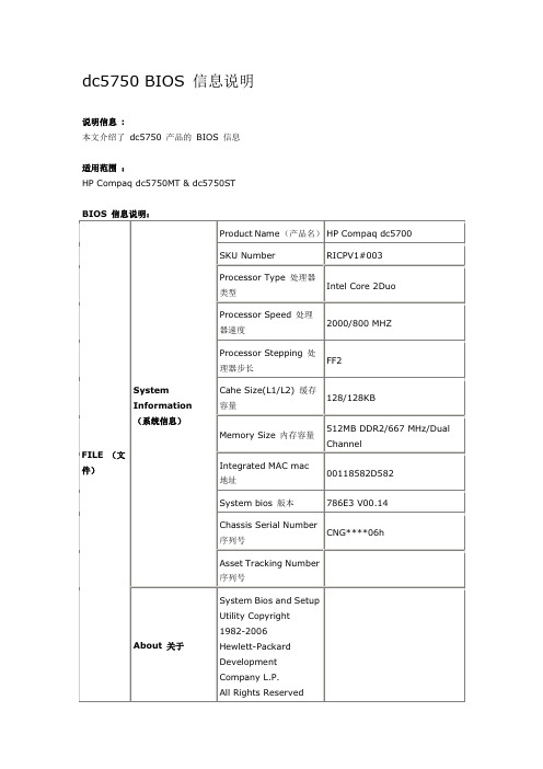
HP Compaq DC5750 BIOS 信息说明
ADVANCED
高级
Power-On Options
启动选项
Post Mode
Quick Boot/Full Boot/Full Boot Every(01~30) Days
Post Messages
Disable/Enable
F9 Prompt
Disable/Enable
F10 Prompt
提示忽略修改并退出
F10=Yes, ESC=No
Save Changes and Exit
保存修改并退出
Are you sure you want to save changes and Exit?
提示保存修改并退出
F10=Yes, ESC=No
STORAGE
存储
Device Configuration
设置安全级别
Setup Password/ None
POWER
电源
OS Power Management
操作系统电源管理
ACPI S3 Hard Disk Reset
Disable/Enable
ACPI S3 PS2 Mouse Wake Up
Disable/Enable
USB Wake on Device Insertion
Disable/Enable
UniqueSleepStateBlink Rates
Disable/Enable
Hardware Power Management
硬件电源管理
SATA Power Management
SATA电源管理
Disable/Enable
Thermal热量
Fan Idle Mode
【霍尼韦尔】Honeywell产品资料

1.1中心管理服务器HUS-VMSHUS-VMS是系统核心服务器,主要包含数据中心管理、报警事件管理、视频流管理、预案编程管理等。
数据中心管理实现站点架构、用户管理、设备配置、权限分配、信息查询等功能;报警事件管理接收报警信息、事件内容、状态变化等信息,对不同类型的前端设备发出操作指令和控制信息,兼容不同类型的通信方式和多种通信格式,对信息内容具备本地缓存功能;视频流管理实现在不同网络带宽条件下大规模视频流媒体传输的控制和优化;预案编程管理提供预案解析、状态监控、规则管理等功能,实现应急情况下的自动执行预案规则,直接交互式的用户界面,及时干预和阻止异常事件。
产品特点•系统集成平台核心单元,无缝集成安防系统•高稳定性、高保障性、高性价比的运行保障•数字化、网络化、集成化、智能化融入一体•基于用户的预案编程、应急指挥、远程管理•虚拟矩阵切换系统提供数字化系统便捷操作•分布式体系架构适合行业用户多级联网管理•矢量电子地图提供GIS、CAD等图精确定位•软件硬件相互融合提供一站式系统运行保障规格参数系统参数⏹操作系统:Windows Server 2008 标准版 64位⏹数据库:SQL Server 2008 标准版64位⏹处理器(CPU):Intel 四核 Xeon 处理器⏹内存:4 GB DDR3 1333 MHz⏹硬盘:250GB, 3.5", 7200rpm, SATA II⏹网络:1 Gbps×2 (双千兆网口)用户界面⏹按钮:电源开关,配置/复位按钮⏹指示灯:电源指示:蓝色(正常工作时)HDD工作:黄色(正常工作时)网络激活:绿色(正常激活时)网络状态:绿色、琥珀色、红色(正常、拥堵、故障)尺寸重量⏹尺寸:42.90(H)×434(W)×612.6mm(D),机架安装(1U)⏹重量: 15 kg环境参数⏹电源:100~240VAC, 50~60Hz⏹工作温度:10°C ~ 35°C⏹储存温度:-40°C ~ 65°C⏹相对湿度:10% ~ 85% 非凝结⏹认证证书:CCC, CE, FCC, UL1.2网络存储系统HUS-NVRHUS-NVR是网络视频监控的存储系统,接收前端视频编码设备(如IP摄像机、编码器、DVR等)的数字化视频流,根据管理需求来实现不同类型的录像规则(计划录像、警情录像、手动录像等)。
HSMH-A100-L00J1中文资料
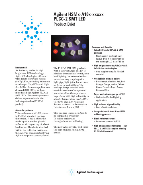
Agilent HSMx-A10x-xxxxx PLCC-2 SMT LEDProduct BriefBackgroundAn industry leader in high brightness LED technology, Agilent Technologies offers a wide range of surface-mount (SMT) LEDs, including Subminia-ture lamps, ChipLEDs and High flux LEDs. As more applications demand SMT LEDs, we have introduced the Agilent PLCC-2 SMT LEDs. These new products deliver top emission in the industry-standard PLCC-2 package.About the productsThis surface-mount LED comes in PLCC-2 standard package dimension. It has a substrate made up of a molded plastic reflector sitting on top of a bent lead frame. The die is attached within the reflector cavity and the cavity is encapsulated by an Agilent proprietary epoxy blend.The PLCC-2 SMT LED productswith a viewing angle of 120° isideal for instruments/switch/iconbacklighting. Its external reflec-tor makes easy coupling withlight pipe/light guide for an even-larger area backlighting. Thepackage design coupled withcareful selection of componentmaterials allow these productsto perform with high reliability ina larger temperature range -40°Cto 100°C. The high reliabilityfeature is crucial to AutomotiveInterior and Indoor ESS.This package is also designed tobe compatible with bothIR-solder reflow andthrough-the-wave soldering.The new Agilent TLED will carrythe part number HSMx-A10x-xxxxx.Features and Benefits•Industry Standard PLCC-2 SMTpackage–No change in existing boardlayout, drop-in replacement forthe existing PLCC-2 SMT LEDs•High brightness using AlInGaP andInGaN dice technologies–Only supplier using TS AlInGaPmaterial•Available in multiple colors–Broad range of colors: Red, Red-Orange, Orange, Amber, Yellow-Green, Emerald Green, Green,Cyan and Blue•Super wide viewing angle at 120°–Well-suited for backlightingapplications•High volume, high reliability–Cost effective solution•Compatible with both IR and TTWsoldering process•Black reflector surface–for reduce contrast in ESS•High brightness performance – onlyPLCC-2 SMT LED supplier offeringTS AlInGaP materialPart Numbers and Typical Product PerformancePart NumberColorDominantViewing Intensity, Iv @ 20mA Vf @ 20mAWavelength λD Angle Min Typ Typical (nm)2θ1/2 (°)(mcd)(mcd)(V)HSMS-A100-J00J1GaP Red 626120415 2.2HSMH-A100-L00J1AS AlGaAs Red 6371201050 1.9HSMC-A100-Q00J1AS AlInGaP Red 62612063100 1.9HSMZ-A100-R00J1TS AlInGaP Red 630120100400 2.2HSMJ-A100-Q00J1AS AlInGaP Red Orange 61512063200 1.9HSMV-A100-R00J1TS AlInGaP Red Orange 617120100350 2.2HSMD-A100-J00J1GaP Orange 602120415 2.2HSML-A100-Q00J1AS AlInGaP Orange 60512063160 1.9HSMY-A100-J00J1GaP Amber 585120415 2.2HSMA-A100-Q00J1AS AlInGaP Amber 59012063100 1.9HSMU-A100-R00J1TS AlInGaP Amber 592120100270 2.2HSMG-A100-J02J1GaP Yellow 569120418 2.2HSMG-A100-H01J1GaP Emerald Green 560120 2.58 2.2HSMM-A100-S00J1InGaN Green 525120160280 3.7HSMK-A100-S00J1InGaN Cyan 505120160280 3.5HSMB-A100-J00J1GaN Blue 462120415 4.0HSMN-A100-P00J1InGaN Blue47012040703.5Notes:1.The luminous intensity l V , is measured at the mechanical axis of the lamp package. The actual peak of the spatial radiation pattern may not be aligned with this axis.2.The dominant wavelength, λD , is derived from the CIE Chromaticity Diagram and represents the color of the device.3.θ1/2 is the off-axis angle where the luminous intensity is 1/2 the peak intensity.Special Product Features and Benefits •Mold Clamp–provides highest reliability performance by eliminating leadframe-epoxy delamination after solder reflow •Reflector Step Down–perfect SMT pick-up due to epoxy overfill being eliminated•Package Bottom Chamfer–perfect lead forming giving high reliability performance (no lead over-formed), and no “tomb-stoning ” defect after solder reflow Target Markets and Applications •Interior automotive–Instrument panel backlighting –Central console backlighting –Cabin backlightingFor product information and a complete list of Agilent contacts and distributors, please go to our web site./semiconductorsE-mail: SemiconductorSupport@ Data subject to change.Copyright © 2002 Agilent Technologies, Inc.February 13, 20025988-5616EN•Electronic Signs and Signals –Interior full color sign –Variable message sign •Office Automation, Electrical Appliances, Industrial Equipment –Front panel backlighting –Push button backlighting –Display backlighting。
SDS9-6CNCH1D数控系统规格说明书20111216
规格说明书 specification
广州市诺信数字测控设备有限公司 LOK SHUN CNC EQUIPMENT LTD.
广州市诺信数字测控设备有限公司
系统简介
SDS9‐6CNCH1D 数控系统以 32 位微处理嵌入式 芯片作为系统主控模块的核心,其功能强大、内置 资源丰富,配以 1024x768 分辨率的液晶彩屏用于 用户加工交互操作显示;以高精度浮点 DSP 和 CPLD 作为加工插补模块的核心;综合运用了实时嵌入式 系统技术、DSP 技术、CPLD 技术、高速高精度光栅 尺测量技术、以太网传输技术等。本产品可配套雕 刻机、雕铣机,主要应用于中端数控机床市场。
第 1 位:(信号类型)
符号
规格
A
脉冲型
第 2 位:(液晶屏)
符号
规格
C
12.1 寸彩色液晶屏
第 3 位:(按键键盘类型)
符号
规格
B
通用编辑功能一体化键盘
第 4 位:(I/O 控制盒类型)
符号
规格
B
支持 36 路输入,36 路输出接口
第 5 位:(系统箱类型)
符号
规格
0
不带控制器箱体
A
LokShun(9-6CNCH)控制器箱体
自动对刀仪
自动对刀长度补偿
△
自动对刀半径补偿
△
语言
中文
○
英文
○
插补周期(ms)
0.5ms(最小)
轨迹前瞻(条)
100
高速断点
条号断点和刀号断点
○(5000 条/s)
2
广州市诺信数字测控设备有限公司
目录文件管理系统 子程序调用 宏程序调用 单节功能 程序预演功能 程序 MDI 功能 程序手工编辑功能 暂停功能 孔加工循环 主轴任意点定位 刀具补偿
Innolux-群创 CONNECTOR
连接器P/N
107C51-0000RA-G4 107C51-0000RA-G4 093G30-B0001A 093G30-B2001A 093G30-B0001A FI-R51S-HF MSAKT2407P30HA 093G30-B0001A
FH23-39S-0.3SHW (05)
液晶屏P/N
M260J1-L01 M240J1-L03 M240J1-L02 M240J1-L01 M236H5-L0A M236H5-L02 M236H5-L01 M236H3-LA2 M236H3-L02 M236H3-L01 M236H1-L08 M236H1-L07 M236H1-L01 M220Z3-LA1 M220Z3-L07 M220Z3-L03 M220Z1-L09 M220Z1-L08 M220Z1-L07 M220Z1-L06 M220Z1-L05 M220Z1-L03 M220Z1-L02 M220Z1-L01 M220J1-L01 M216H5-L01 M216H1-L07 M216H1-L05 M216H1-L03 M216H1-L02 M216H1-L01 M215H3-LA1 M215H3-L01 M215H1-L03 M215H1-L02 M215H1-L01 M201U1-L01 M201P1-L03 M201P1-L01 M200O3-LA1 M200O3-L01 M200O1-L05 M200O1-L03 M200O1-L02 M200O1-L01 M190Z1-P01 M190Z1-L03 M190Z1-L01 M190E6-L01 M190E5-L0G M190E5-L0E M190E5-L0B M190E5-L0A M190E3-L02 M190E3-L01 M190E2-L01 M190A1-L10 M190A1-L0G M190A1-L0F M190A1-L0C M190A1-L0B M190A1-L0A M190A1-L09 M190A1-L08 M190A1-L07 M190A1-L06 M190A1-L05 M190A1-L03 M190A1-L02 M190A1-L01
HFBR1412C资料
46Transmitters and receivers are directly compatible with popular “industry-standard” connectors: ST, SMA, SC and FC. They are completely specified with multiple fiber sizes; including50/125 µm, 62.5/125 µm, 100/ 140 µm, and 200 µm.Complete evaluation kits are available for ST and SMA product offerings; including transmitter, receiver, connectored cable, and technical literature. In addition, ST and SMA connectored cables are available for evaluation.Low Cost, Miniature FiberOptic Components with ST®,SMA, SC and FC PortsTechnical DataHFBR-0400 SeriesFeatures• Meets IEEE 802.3 Ethernet and 802.5 Token Ring Standards• Low Cost Transmitters and Receivers• Choice of ST®, SMA, SC or FC Ports• 820 nm Wavelength Technology• Signal Rates up to 175 Megabaud• Link Distances up to 4 km • Specified with 50/125 µm, 62.5/125 µm, 100/140 µm, and 200 µm HCS® Fiber• Repeatable ST Connections within 0.2 dB Typical• Unique Optical Port Design for Efficient Coupling• Auto-Insertable and Wave Solderable• No Board Mounting Hard-ware Required• Wide Operating Temperature Range-40°C to 85°C• AlGaAs Emitters 100%Burn-In Ensures High Reliability• Conductive Port Option with the SMA and ST Threaded Port Styles Applications• Local Area Networks• Computer to Peripheral Links• Computer Monitor Links • Digital Cross Connect Links • Central Office Switch/PBX Links• Video Links• Modems and Multiplexers • Suitable for Tempest Systems• Industrial Control Links DescriptionThe HFBR-0400 Series of compo-nents is designed to provide cost effective, high performance fiber optic communication links for information systems and industrial applications with link distances of up to 4 kilometers. With the HFBR-24X6, the 125 MHz analog receiver, data rates of up to 175 megabaud are attainable.ST® is a registered trademark of AT&T. HCS®is a registered trademark of the SpecTran Corporation.5965-1655E (1/97)47HFBR-0400 Series Part Number GuideHFBR X4XXaa1 = Transmitter Option T (Threaded Port Option)2 = ReceiverOption C (Conductive Port Receiver Option)Option M (Metal Port Option)4 = 820 nm Transmitter andOption K (Kinked Lead Option)Receiver Products TA = Square pinout/straight lead TB = Square pinout/bent leads0 = SMA, Housed HA = Diamond pinout/straight leads 1 = ST, Housed HB = Diamond pinout/bent leads 2 = FC, Housed E = SC, Housed2 = Tx, Standard Power3 = SMA Port, 90 deg. Bent Leads4 = Tx, High Power4 = ST Port, 90 deg. Bent Leads 2 = Rx,5 MBd, TTL Output5 = SMA Port, Straight Leads6 = Rx, 125 MHz, Analog Output6 = ST Port, Straight LeadsLINK SELECTION GUIDEData Rate (MBd)Distance (m)Transmitter Receiver Fiber Size (µm)Evaluation Kit 51500HFBR-14X2HFBR-24X2200 HCS N/A52000HFBR-14X4HFBR-24X262.5/125HFBR-04X0202700HFBR-14X4HFBR-24X662.5/125HFBR-0414,HFBR-0463322200HFBR-14X4HFBR-24X662.5/125HFBR-0414551400HFBR-14X4HFBR-24X662.5/125HFBR-0414125700HFBR-14X4HFBR-24X662.5/125HFBR-0416155600HFBR-14X4HFBR-24X662.5/125HFBR-0416175500HFBR-14X4HFBR-24X662.5/125HFBR-0416For additional information on specific links see the following individual link descriptions. Distances measured over temperature range from 0 to 70°C.Applications Support GuideThis section gives the designer information necessary to use the HFBR-0400 series components tomake a functional fiber-optic transceiver. HP offers a wide selection of evaluation kits for hands-on experience with fiber-optic products as well as a wideApplication LiteratureTitleDescriptionHFBR-0400 Series Transmitter & Receiver Reliability DataReliability DataApplication Bulletin 73Low Cost Fiber Optic Transmitter & Receiver Interface Circuits Application Bulletin 78Low Cost Fiber Optic Links for Digital Applications up to 155 MBdApplication Note 1038Complete Fiber Solutions for IEEE 802.3 FOIRL, 10Base-FB and 10 Base-FL Application Note 1065Complete Solutions for IEEE 802.5J Fiber-Optic Token Ring Application Note 1073HFBR-0319 Test Fixture for 1X9 Fiber Optic TransceiversApplication Note 1086Optical Fiber Interconnections in Telecommunication Productsrange of application notes com-plete with circuit diagrams and board layouts. Furthermore, HP’s application support group is always ready to assist with any design consideration.HFBR-0400 Series Evaluation KitsHFBR-0410 ST Evaluation Kit Contains the following :• One HFBR-1412 transmitter • One HFBR-2412 five megabaud TTL receiver• Three meters of ST connec-tored 62.5/125 (µm fiber optic cable with low cost plastic ferrules.• Related literatureHFBR-0414 ST Evaluation Kit Includes additional components to interface to the transmitter and receiver as well as the PCB to reduce design time.Contains the following:• One HFBR-1414T transmitter • One HFBR-2416T receiver• Three meters of ST connec-tored 62.5/125 µm fiber optic cable• Printed circuit board• ML-4622 CP Data Quantizer • 74ACTllOOON LED Driver• LT1016CN8 Comparator• 4.7 µH Inductor• Related literatureHFBR-0400 SMA Evaluation KitContains the following :• One HFBR-1402 transmitter • One HFBR-2402 five megabaud TTL receiver• Two meters of SMA connectored 1000 µm plastic optical fiber• Related literature HFBR-0416 Evaluation KitContains the following:• One fully assembled 1x9transceiver board for 155 MBdevaluation including:-HFBR-1414 transmitter-HFBR-2416 receiver-circuitry• Related literatureHFBR-0463 Ethernet MAUEvaluation KitContains the following:• One fully assembled MediaAttachment Unit (MAU) boardwhich includes:-HFBR-1414 transmitter-HFBR-2416 receiver-HFBR-4663 IC• Related literatureNote: Cable not included. OrderHFBR-BXS010 seperately (2pieces)Package and HandlingInformationPackage InformationAll HFBR-0400 Seriestransmitters and receivers arehoused in a low-cost, dual-inlinepackage that is made of highstrength, heat resistant, chem-ically resistant, and UL 94V-Oflame retardant ULTEM® (plastic(UL File #E121562). Thetransmitters are easily identifiedby the light grey color connectorport. The receivers are easilyidentified by the dark grey colorconnector port. (Black color forconductive port.) The package isdesigned for auto-insertion andwave soldering so it is ideal forhigh volume productionapplications.Handling and DesignInformationEach part comes with a protectiveport cap or plug covering theoptics. These caps/plugs will varyby port style. When soldering, itis advisable to leave the protec-tive cap on the unit to keep theoptics clean. Good systemperformance requires clean portoptics and cable ferrules to avoidobstructing the optical path.Clean compressed air often issufficient to remove particles ofdirt; methanol on a cotton swabalso works well.Recommended Chemicals forCleaning/DegreasingHFBR-0400 ProductsAlcohols: methyl, isopropyl,isobutyl. Aliphatics: hexane,heptane, Other: soap solution,naphtha.Do not use partially halogenatedhydrocarbons such as 1,1.1trichloroethane, ketones such asMEK, acetone, chloroform, ethylacetate, methylene dichloride,phenol, methylene chloride, orN-methylpyrolldone. Also, HPdoes not recommend the use ofcleaners that use halogenatedhydrocarbons because of theirpotential environmental harm.Ultem® is a registered Trademark of the GE corporation.48Mechanical Dimensions HFBR-0400 SMA SeriesHFBR-X45XHFBR-X40XDIAPART MARKINGYYWW8.6(0.34)DIADIA PINCIRCLE3.81(0.15)DIAPINS 2,3,6,70.46(0.018)DIA.INDICATOR4950Mechanical Dimensions HFBR-0400 ST SeriesHFBR-X46XHFBR-X41X8.6(0.34)NOTE 2DIANOTE: ALL DIMENSIONS IN MILLIMETRES AND (INCHES).3.81(0.15)DIA0.46(0.018)INDICATOR51Mechanical Dimensions HFBR-0400T Threaded ST SeriesHFBR-X46XTHFBR-X41XT3.81(0.15)DIAINDICATOR0.46(0.018)NOTE 27.68.6(0.34)Mechanical Dimensions HFBR-0400 FC SeriesMechanical Dimensions HFBR-0400 SC Series3.81(0.15)INDICATORM8 x 0.75 6GTHREAD (METRIC)(0.14)HFBR-X4EX5253Figure 1. HFBR-0400 ST Series Cross-Sectional View.Panel Mount HardwarePort Cap HardwareHFBR-4402: 500 SMA Port CapsHFBR-4120: 500 ST Port Plugs (120 psi)HFBR-4412: 500 FC Port Caps HFBR-4417: 500 SC Port PlugsTYP DIA1.65(0.065)WASHERTYP DIA1.65(0.065)HFBR-4401: for SMA PortsHFBR-4411: for ST Ports(Each HFBR-4401 and HFBR-4411 kit consists of 100 nuts and 100 washers.)OptionsIn addition to the various portstyles available for the HFBR-0400 series products, there are also several extra options that can be ordered. To order an option, simply place the corre-sponding option number at the end of the part number. For instance, a metal-port option SMA receiver would be HFBR-2406M. You can add any number of options in series at the end of a part number. Please contact your local sales office for further information or browse HP’s fiber optics home page at http:// /go/fiberOption T (Threaded Port Option)• Allows ST style port com-ponents to be panel mounted.• Compatible with all current makes of ST multimode connectors• Mechanical dimensions are compliant with MIL-STD-83522/13• Maximum wall thickness when using nuts and washers from the HFBR-4411 hardware kit is 2.8 mm (0.11 inch)• Available on all ST ports Option C (Conductive PortReceiver Option)• Designed to withstand electro-static discharge (ESD) of 25kV to the port• Significantly reduces effect of electromagnetic interference (EMI) on receiver sensitivity • Allows designer to separate thesignal and conductive portgrounds• Recommended for use in noisyenvironments• Available on SMA and threadedST port style receivers onlyOption M (Metal Port Option)• Nickel plated aluminum con-nector receptacle• Designed to withstand electro-static discharge (ESD) of 15kVto the port• Significantly reduces effect ofelectromagnetic interference(EMI) on receiver sensitivity• Allows designer to separate thesignal and metal port grounds• Recommended for use in verynoisy environments• Available on SMA, FC, ST, andthreaded ST portsOption K (Kinked LeadOption)• Grounded outside 4 leads are“kinked”• Allows components to stayanchored in the PCB duringwave solder and aqueous washprocessesOptions TA, TB, HA, HB(Active Device MountOptions)(These options are unrelated tothe threaded port option T.)• All metal, panel mountablepackage with a 3 or 4 pinreceptacle end• Available for HFBR-14X4, 24X2and 24X6 components• Choose from diamond orsquare pinout, straight or bentleads ADM Picture• TA = Square pinout/straightleadsTB = Square pinout/bent leadsHA = Diamond pinout/straightleadsHB = Diamond pinout/bentleadsDuplex OptionIn addition to the standardoptions, some HFBR-0400 seriesproducts come in a duplex con-figuration with the transmitter onthe left and the receiver on theright. This option was designedfor ergonomic and efficientmanufacturing. The followingpart numbers are available in theduplex option:HFBR-5414 (Duplex ST)HFBR-5414T (Duplex ThreadedST)HFBR-54E4 (Duplex SC)54Typical Link Data HFBR-0400 SeriesDescriptionThe following technical data is taken from 4 popular links using the HFBR-0400 series: the 5 MBd link, Ethernet 20 MBd link, Token Ring 32 MBd link, and the 155 MBd link. The data given corresponds to transceiver solu-tions combining the HFBR-0400series components and variousrecommended transceiver designcircuits using off-the-shelfelectrical components. This datais meant to be regarded as anexample of typical link perform-ance for a given design and doesnot call out any link limitations.Please refer to the appropriateapplication note given for eachlink to obtain more information.5 MBd Link (HFBR-14XX/24X2)Link Performance -40°C to +85°C unless otherwise specifiedNotes:1. OPB at T A = -40 to 85°C, V CC = 5.0 V dc, I F ON = 60 mA. P R = -24 dBm peak.2. Synchronous data rate limit is based on these assumptions: a) 50% duty factor modulation, e.g., Manchester I or BiPhaseManchester II; b) continuous data; c) PLL Phase Lock Loop demodulation; d) TTL threshold.3. Asynchronous data rate limit is based on these assumptions: a) NRZ data; b) arbitrary timing-no duty factor restriction; c) TTLthreshold.55565 MBd Logic Link DesignIf resistor R 1 in Figure 2 is 70.4Ω, a forward current I F of 48 mA is applied to the HFBR-14X4 LED transmitter. With I F =48 mA the HFBR-14X4/24X2logic link is guaranteed to work with 62.5/125 µm fiber optic cable over the entire range of 0to 1750 meters at a data rate of dc to 5 MBd, with arbitrary data format and pulse width distortion typically less than 25%. Bysetting R 1 = 115 Ω, the transmit-ter can be driven with I F =30mA,if it is desired to economize on power or achieve lower pulse distortion.The following example will illus-trate the technique for selecting the appropriate value of I F and R 1.Maximum distance required=400 meters. From Figure 3 the drive current should be 15 mA.From the transmitter dataV F =1.5 V (max.) at I F = 15 mA as shown in Figure 9.V CC - V F 5 V - 1.5 V R 1 = ––––––– = –––––––––I F 15 mA R 1 = 233␣ΩThe curves in Figures 3, 4, and 5are constructed assuming no in-line splice or any additional system loss. Should the link consists of any in-line splices,these curves can still be used to calculate link limits provided they are shifted by the additionalsystem loss expressed in dB. For example, Figure 3 indicates that with 48 mA of transmitter drive current, a 1.75 km link distance is achievable with 62.5/125 µm fiber which has a maximum attenuation of 4 dB/km. With 2dB of additional system loss, a 1.25 km link distance is still achievable.Figure 2. Typical Circuit Configuration.57Figure 6. Propagation Delay through System with One Meter of Cable.Figure 8. System Propagation Delay Test Circuit and Waveform Timing Definitions.Figure 3. HFBR-1414/HFBR-2412Link Design Limits with 62.5/125 µm Cable.Figure 4. HFBR-14X2/HFBR-24X2Link Design Limits with 100/140 µm Cable.Figure 7. Typical Distortion of Pseudo Random Data at 5 Mb/s.Figure 5. HFBR-14X4/HFBR-24X2Link Design Limits with 50/125 µmCable.0-1-2-3-4-5-610 L O G (t /t o ) N O R M A L I Z E D T R A N S M I T T E R C U R R E N T (d B )LINK LENGTH (km)I F T R A N S M I T T E R F O R W A R D C U R R E N T (mA )605075-22-21-20-19-18-17-16-15-14-13-12P R – RECEIVER POWER – dBmt P H L O R t P H L P R O P O G A T I O N D E L A Y –n s706560555045403530252055-22-21-20-19-18-17-16-15-14-13-12P R – RECEIVER POWER – dBmt D – N R Z D I S T O R T I O N – n s50454035302520Ethernet 20 MBd Link (HFBR-14X4/24X6)(refer to Application Note 1038 for details)Typical Link PerformanceNotes:1. Typical data at T A = 25°C, V CC = 5.0 V dc.2. Typical performance of circuits shown in Figure 1 and Figure 3 of AN-1065 (see applications support section) 58155 MBd Link (HFBR-14X4/24X6)(refer to Application Bulletin 78 for details)Typical Link PerformanceNotes:1. Typical data at T A = 25°C, V CC = 5.0 V dc, PECL serial interface.2. Typical OPB was determined at a probability of error (BER) of 10-9. Lower probabilities of error can be achieved with short fibersthat have less optical loss.5960HFBR-14X2/14X4 Low-Cost High-Speed TransmittersDescriptionThe HFBR-14XX fiber optic transmitter contains an 820 nm AlGaAs emitter capable of efficiently launching optical power into four different optical fiber sizes: 50/125 µm, 62.5/125µm, 100/140 µm, and 200 µm HCS ®. This allows the designer flexibility in choosing the fiber size. The HFBR-14XX is designed to operate with the Hewlett-Packard HFBR-24XX fiber optic receivers.The HFBR-14XX transmitter’s high coupling efficiency allows the emitter to be driven at low current levels resulting in lowpower consumption and increased reliability of the transmitter. The HFBR-14X4 high power transmit-ter is optimized for small sizefiber and typically can launch -15.8 dBm optical power at60mA into 50/125 µm fiber and -12 dBm into 62.5/125µm fiber.The HFBR-14X2 standardtransmitter typically can launch -12 dBm of optical power at 60mA into 100/140 µm fiber cable. It is ideal for large size fiber such as 100/140 µm. The high launched optical power level is useful for systems where star couplers, taps, or inline connec-tors create large fixed losses.Consistent coupling efficiency is assured by the double-lens optical system (Figure 1). Power coupled into any of the three fiber types varies less than 5 dB from part to part at a given drive current and temperature. Consistent coupling efficiency reduces receiver dynamic range requirements which allows for longer link lengths.Absolute Maximum RatingsHoused ProductUnhoused Product61HFBR-14X2 Output Power Measured Out of 1 Meter of CableElectrical/Optical Specifications -40°C to +85°C unless otherwise specified.CAUTION: The small junction sizes inherent to the design of these components increase the components’susceptibility to damage from electrostatic discharge (ESD). It is advised that normal static precautions be taken in handling and assembly of these components to prevent damage and/or degradation which may be induced by ESD.HFBR-14X4 Output Power Measured out of 1 Meter of Cable14X2/14X4 Dynamic CharacteristicsParameter Symbol Min.Typ.[2]Max.Units Conditions Reference Rise Time, Fall Time t r, t f 4.0 6.5nsec I F = 60 mA Note 7, (10% to 90%)No Pre-bias Figure 12Rise Time, Fall Time t r, t f 3.0nsec I F = 10 to Note 7, (10% to 90%)100 mA Figure 11 Pulse Width Distortion PWD0.5nsec Figure 11 Notes:1. For I FPK > 100 mA, the time duration should not exceed 2 ns.2. Typical data at T A = 25°C.3. Thermal resistance is measured with the transmitter coupled to a connector assembly and mounted on a printed circuit board.4. D is measured at the plane of the fiber face and defines a diameter where the optical power density is within 10 dB of themaximum.5. P T is measured with a large area detector at the end of 1 meter of mode stripped cable, with an ST® precision ceramic ferrule (MIL-STD-83522/13) for HFBR-1412/1414, and with an SMA 905 precision ceramic ferrule for HFBR-1402/1404.6. When changing µW to dBm, the optical power is referenced to 1 mW (1000 µW). Optical Power P (dBm) = 10 log P (µW)/1000µW.7. Pre-bias is recommended if signal rate >10 MBd, see recommended drive circuit in Figure 11.8. Pins 2, 6 and 7 are welded to the anode header connection to minimize the thermal resistance from junction to ambient. To furtherreduce the thermal resistance, the anode trace should be made as large as is consistent with good RF circuit design.9. Fiber NA is measured at the end of 2 meters of mode stripped fiber, using the far-field pattern. NA is defined as the sine of the halfangle,determined at 5% of the peak intensity point. When using other manufacturer’s fiber cable, results will vary due to differing NA values and specification methods.All HFBR-14XX LED transmitters are classified as IEC 825-1 Accessible Emission Limit (AEL) Class 1 based upon the current proposed draft scheduled to go in to effect on January 1, 1997. AEL Class 1 LED devices are considered eye safe. Contact your Hewlett-Packard sales representative for more information.CAUTION: The small junction sizes inherent to the design of these components increase the components’susceptibility to damage from electrostatic discharge (ESD). It is advised that normal static precautions be taken in handling and assembly of these components to prevent damage and/or degradation which may be induced by ESD.6263Recommended Drive CircuitsThe circuit used to supply current to the LED transmitter cansignificantly influence the optical switching characteristics of the LED. The optical rise/fall times and propagation delays can be improved by using the appro-priate circuit techniques. The LED drive circuit shown inFigure 11 uses frequency com-pensation to reduce the typical rise/fall times of the LED and a small pre-bias voltage to minimize propagation delay differences that cause pulse-width distortion.The circuit will typically produce rise/fall times of 3 ns, and a total jitter including pulse-width dis-tortion of less than 1 ns. This circuit is recommended for appli-cations requiring low edge jitteror high-speed data transmission at signal rates of up to 155 ponent values for this circuit can be calculated for different LED drive currents using the equations shown below. For additional details about LED drive circuits, the reader is encouraged to read Hewlett-Packard Application Bulletin 78and Application Note 1038.()()(V CC - V F ) + 3.97 (V CC - V F - 1.6 V)(5 - 1.84) + 3.97 (5 - 1.84 - 1.6)R y = –––––––––––––––––––––––––––––––R y = –––––––––––––––––––––––––––––I F ON (A)0.100 1 R y 3.16 + 6.19R X1 = – ––––R y = ––––––––––– = 93.5 Ω2 3.970.1001 93.5R EQ2(Ω) = R X1 - 1R X1 = – ––––= 11.8 Ω2 3.97R X2 = R X3 = R X4 = 3(R EQ2)R EQ2 = 11.8 - 1 = 10.8 Ω2000(ps)C(pF) = ––––––––R X2 = R X3 = R X4 = 3(10.8) = 32.4 Ω R X1(Ω)2000 psExample for I F ON = 100 mA: V F can be C = ––––––– = 169 pF11.8 Ωobtained from Figure 9 (= 1.84 V ).64Figure 9. Forward Voltage and Current Characteristics.Figure 12. Test Circuit for Measuring t r , t f .Figure 11. Recommended Drive Circuit.Figure 10. Normalized TransmitterOutput vs. Forward Current.P (I F ) – P (60 m A ) – R E L A T I V E P O W E R R A T I O02.00.80I F – FORWARD CURRENT – mA2040801.60.41.2601001.81.41.00.60.230507090P (I F ) – P (60 m A ) – R E L A T I V E P O W E R R A T I O – d B-7.0-5.0-4.0-3.0-2.0-1.000.81.01.42.03.065HFBR-24X2 Low-Cost 5MBd Receiver DescriptionThe HFBR-24X2 fiber optic receiver is designed to operate with the Hewlett-Packard HFBR-14XX fiber optic transmitter and 50/125 µm, 62.5/125 µm, 100/140 µm, and 200 µm HCS ® fiber optic cable. Consistent coupling into the receiver is assured by the lensed optical system (Figure 1).Response does not vary with fiber size ≤0.100 µm.The HFBR-24X2 receiver incor-porates an integrated photo IC containing a photodetector and dc amplifier driving an open-collector Schottky output transistor. The HFBR-24X2 isHoused ProductUnhoused Productdesigned for direct interfacing to popular logic families. The absence of an internal pull-up resistor allows the open-collector output to be used with logicfamilies such as CMOS requiring voltage excursions much higher than V CC .Both the open-collector “Data”output Pin 6 and V CC Pin 2 are referenced to “Com” Pin 3, 7. The “Data” output allows busing,strobing and wired “OR” circuit configurations. The transmitter is designed to operate from a single +5 V supply . It is essential that a bypass capacitor (0.1 µF ceramic) be connected from Pin 2 (V CC ) to Pin 3 (circuit common) of the receiver.Absolute Maximum RatingsPIN FUNCTION 1234V CC (5 V)COMMON DATA COMMONElectrical/Optical Characteristics -40°C to + 85°C unless otherwise specifiedFiber sizes with core diameter ≤100 µm and NA ≤0.35, 4.75 V ≤V CC≤5.25 VParameter Symbol Min.Typ.[3]Max.Units Conditions Reference High Level Output Current I OH5250µA V O = 18P R < -40 dBmLow Level Output Voltage V OL0.40.5V I O = 8 mAP R > -24 dBmHigh Level Supply Current I CCH 3.5 6.3mA V CC = 5.25 VP R < -40 dBmLow Level Supply Current I CCL 6.210mA V CC = 5.25 VP R > -24 dBmEquivalent N.A.NA0.50Optical Port Diameter D400µm Note 4 Dynamic Characteristics-40°C to +85°C unless otherwise specified; 4.75 V ≤V CC≤5.25 V; BER ≤10-9Notes:1. 2.0 mm from where leads enter case.2. 8 mA load (5 x 1.6 mA), R L = 560 Ω.3. Typical data at T A = 25°C, V CC = 5.0 Vdc.4. D is the effective diameter of the detector image on the plane of the fiber face. The numerical value is the product of the actualdetector diameter and the lens magnification.5. Measured at the end of 100/140 µm fiber optic cable with large area detector.6. Propagation delay through the system is the result of several sequentially-occurring phenomena. Consequently it is a combinationof data-rate-limiting effects and of transmission-time effects. Because of this, the data-rate limit of the system must be described in terms of time differentials between delays imposed on falling and rising edges.7. As the cable length is increased, the propagation delays increase at 5 ns per meter of length. Data rate, as limited by pulse widthdistortion, is not affected by increasing cable length if the optical power level at the receiver is maintained.CAUTION: The small junction sizes inherent to the design of these components increase the components’HFBR-24X6 Low-Cost 125 MHz Receiver DescriptionThe HFBR-24X6 fiber optic receiver is designed to operate with the Hewlett-Packard HFBR-14XX fiber optic transmitters and 50/125 µm, 62.5/125 µm, 100/ 140 µm and 200 µm HCS® fiber optic cable. Consistent coupling into the receiver is assured by the lensed optical system (Figure 1). Response does not vary with fiber size for core diameters of 100 µm or less.The receiver output is an analog signal which allows follow-on circuitry to be optimized for a variety of distance/data rate requirements. Low-cost external components can be used to convert the analog output to logic compatible signal levels for various data formats and data rates up to 175 MBd. This distance/data rate tradeoff results in increased optical power budget at lower data rates which can be used for additional distance or splices.The HFBR-24X6 receiver contains a PIN photodiode and low noise transimpedance pre-amplifier integrated circuit. The HFBR-24X6 receives an optical signal and converts it to an analog voltage. The output is a buffered emitter-follower. Because the signal amplitude from the HFBR-24X6 receiver is much larger than from a simple PIN photodiode, it is less susceptible to EMI, especially at high signaling rates. For very noisy environments, the conductive or metal port option is recommended.A receiver dynamic range of 23 dB over temperature is achievable (assuming 10-9 BER).The frequency response is typically dc to 125 MHz. Although the HFBR-24X6 is an analog receiver, it is compatible with digital systems. Please refer to Application Bulletin 78 for simple and inexpensive circuits that operate at 155 MBd or higher. The recommended ac coupled receiver circuit is shown in Figure 12. It is essential that a 10 ohm resistor be connected between pin 6 and the power supply, and a 0.1µF ceramic bypass capacitor be connected between the power supply and ground. In addition, pin 6 should be filtered to protect theFigure 11. Simplified Schematic Diagram.Housed ProductUnhoused Productreceiver from noisy host systems. Refer to AN 1038, 1065, or AB 78 for details.PINFUNCTION12*34*SIGNALV EEV CCV EEINDICATORCCEE* PINS 3 AND 7 ARE ELECTRICALLYCONNECTED TO THE HEADER.† PINS 1, 4, 5, AND 8 ARE ISOLATED FROMTHE INTERNAL CIRCUITRY, BUT AREELECTRICALLY CONNECTED TO EACH OTHER.POSITIVE SUPPLY ANALOG SIGNALNEGATIVE SUPPLY。
SN65HVD233MDREP中文资料
This device has limited built-in ESD protection. The leads should be shorted together or the device placed in conductive foam duቤተ መጻሕፍቲ ባይዱing storage or handling to prevent electrostatic damage to the MOS gates.
3.3-V CAN TRANSCEIVER
1
FEATURES
Bus-Pin Fault Protection Exceeds ±36 V Bus-Pin ESD Protection Exceeds 16-kV HBM Compatible With ISO 11898 Signaling Rates(1) up to 1 Mbps Extended –7-V to 12-V Common-Mode Range High-Input Impedance Allows for 120 Nodes LVTTL I/Os Are 5-V Tolerant Adjustable Driver Transition Times for Improved Signal Quality Unpowered Node Does Not Disturb the Bus Low-Current Standby Mode . . . 200-µA Typical Thermal Shutdown Protection Power-Up/Down Glitch-Free Bus Inputs and Outputs – High Input Impedance With Low VCC – Monolithic Output During Power Cycling Loopback for Diagnostic Functions Available DeviceNet Vendor ID #806
- 1、下载文档前请自行甄别文档内容的完整性,平台不提供额外的编辑、内容补充、找答案等附加服务。
- 2、"仅部分预览"的文档,不可在线预览部分如存在完整性等问题,可反馈申请退款(可完整预览的文档不适用该条件!)。
- 3、如文档侵犯您的权益,请联系客服反馈,我们会尽快为您处理(人工客服工作时间:9:00-18:30)。
Document Title Document No. HSD101PWW2 Standard Product Specification Page No. Revision 1/28 1.0
TO
: Feb, 22, 2012
Date :
H a n n Sta r Di s p l a y C o rp .
Document Title Document No. HSD101PWW2 Standard Product Specification Page No. Revision 2/28 1.0
Record of Revisions
1.1 Introduction HannStar Display model HSD101PWW2-A** is a color active matrix thin film transistor (TFT) liquid crystal display (LCD) that uses amorphous silicon TFT as a switching device. This model is composed of a TFT LCD panel, a driving circuit and a back light system. This TFT LCD has a 10.1(16:10) inch diagonally measured active display area with WXGA (1280 horizontal by 800 vertical pixel) resolution. 1.2 Features ■ 10.1 (16:10 diagonal) inch configuration ■ One channel LVDS interface ■ 16.7M (6 bit + Hi FRC) ■ RoHS Compliance ■ Halogen Free 1.3 Applications Handbook Notebook
Package specification ……………………………… General precaution ……………………………………
The information contained in this document is the exclusive property of HannStar Display Corporation. It shall not be disclosed, distributed or reproduced in whole or in part without written permission of HannStar Display Corporation.
Specification 229(Typ) x151 (Typ) 216.96 (H) x 135.6(V) 1280 RGB (H) x 800(V) 0.1695(H) x 0.1695(V) RGB Vertical stripe Normally Black 45 Glare, Anti-Reflection≦1.5%, Hard-Coating (3H) 155g(Max.) White LED 4.56(max) @White pattern PWM duty ratio=100%Vin=3.3V, VLED=12V
H a n n Sta r Di s p l a y C o rp .
Document Title Document No. HSD101PWW2 Standard Product Specification Page No. Revision 5/28 1.0
1.5 Mechanical Information Item Horizontal (H) Module Size Vertical (V) Depth (D) w/o PCB Depth (D) w/ PCB
3.1 Optical specification Item Contrast Response time Rising White luminance (Center Point) Red Green Blue White Symbol Condition CR Tr+Tf YL Rx RY Gx GY Bx BY Wx Wy Hor. Viewing angle Ver. Brightness uniformity ΘL ΘR ΘU ΘD BUNI Θ=0 (9point) CR>10 Θ=0 Normal viewing angle Min. 600 - 550 0.545 0.321 0.299 0.542 0.134 0.083 0.290 0.310 80 80 80 80 - Typ. 800 25 650 0.575 0.351 0.329 0.572 0.164 0.113 0.320 0.340 89 89 89 89 - Max. - 40 - 0.605 0.381 0.359 0.602 0.194 0.143 0.350 0.370 - - - - 1.25 (6) (1)(4) msec cd/m2 Unit Note (1)(2)(4) (1)(3) (1)(4)(5) (IL=22mA)
Min. 228.7 150.7 - -
Typ. 229 151 2.5 4.53
Max. 229.3 151.3 2.7 4.83 155
Unit mm mm mm mm g
Weight 145 - Note : I/F conn Position Depth is 4.88mm (Max)
2.0 ABSOLUTE MAXIMUM RATINGS
Unit mm mm pixels mm
%
g
W
The information contained in this document is the exclusive property of HannStar Display Corporation. It shall not be disclosed, distributed or reproduced in whole or in part without written permission of HannStar Display Corporation.
Interface pin connection Electrical characteristics
Reliability test items ………………………………… Outline dimension …………………………………… Lot mark ……………………………………………...
H a n n Sta r Di s p l a y C o rp .
Document Title Document No. HSD101PWW2 Standard Product Specification Page No. Revision 6/28 1.0
3.0 OPTICAL CHARACTERISTICS
H a n n Sta r Di s p l a y C o rp .
Document Title Document No. HSD101PWW2 Standard Product Specification Page No. Revision 3/28 1.0
Contents
1.0 2.0 3.0 4.0 5.0 6.0 7.0 8.0 9.0 10.0 11.0 General description ………………………………… Absolute maximum ratings……………………………. Optical characteristics.………………………………. Block diagram ……………………………………… …………………………… …………………………… p.4 p.5 p.6 p.10 p.12 p.14 p.21 p.22 p.24 p.25 p.26
Rev.
1.0
Date
Feb, 22, 2012
Sub-Model
A**
Description of change
Formal product specification was first released.
The information contained in this document is the exclusive property of HannStar Display Corporation. It shall not be disclosed, distributed or reproduced in whole or in part without written permission of HannStar Display Corporation.
1.4 General information Item Outline Dimension Display area Number of Pixel Pixel pitch Pixel arrangement Display mode NTSC Surface treatment Weight Back-light Power Consumption Logic and BLU
2.1 Electrical Absolute Rating 2.1.1 TFT LCD Module Item Symbol Logic Supply voltage VDD
Min. -0.3
Max. 4.0
Unit V
Note
2.1.2
Environment Absolute Rating Item Symbol Operating Temperature Topa Storage Temperature Tstg