tm0868非隔离恒压12v200ma电源芯片规格书v10
最新EG8010芯片手册
7. 电气特性 ........................................................................................................................................................... 11
1. 更新典型应用电路图(短路保护 LM393 部分),及应用图中 IR2103 驱动器到 IR2106 驱动器。
2. 添加工频变压器正弦波逆变器应用电路图。 1. 添加 EG8010+IR2110+闭锁功能典型应用图及更新典型应用
电路图参数。
2. 修改图 8.9a RS232 光耦隔离通讯电路中 MAX232 芯片的 9 脚和 10 脚连接。
7.2
典型参数 ........................................................................................................................................................................................................................................................................................ 7
4.1. 引脚定义 ............................................................................................................................................. 5
MAX1771ESA+中文资料
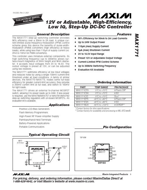
MAX1771
Ordering Information
PART MAX1771CPA MAX1771CSA MAX1771C/D MAX1771EPA MAX1771ESA MAX1771MJA TEMP RANGE 0°C to +70°C 0°C to +70°C 0°C to +70°C -40°C to +85°C -40°C to +85°C -55°C to +125°C PIN-PACKAGE 8 Plastic DIP 8 SO Dice* 8 Plastic DIP 8 SO 8 CERDIP**
ELECTRICAL CHARACTERISTICS
(V+ = 5V, ILOAD = 0mA, TA = TMIN to TMAX, unless otherwise noted. Typical values are at TA = +25°C.) PARAMETER Input Voltage Range Minimum Start-Up Voltage Supply Current Standby Current Output Voltage (Note 1) Output Voltage Line Regulation (Note 2) Output Voltage Load Regulation (Note 2) Maximum Switch On-Time Minimum Switch Off-Time Efficiency tON(max) tOFF(min) V+ = 5V, VOUT = 12V, ILOAD = 500mA, Circuit of Figure 2a MAX1771C Reference Voltage VREF IREF = 0µA MAX1771E MAX1771M REF Load Regulation REF Line Regulation FB Trip Point Voltage VFB 0µA ≤ IREF ≤ 100µA 3V ≤ V+ ≤ 16.5V MAX1771C MAX1771E MAX1771M 1.4700 1.4625 1.4550 MAX1771C/E MAX1771M 1.4700 1.4625 1.4550 V+ = 16.5V, SHDN = 0V (normal operation) V+ = 10V, SHDN ≥ 1.6V (shutdown) V+ = 16.5V, SHDN ≥ 1.6V (shutdown) V+ = 2V to 12V, over full load range, Circuit of Figure 2a V+ = 5V to 7V, VOUT = 12V ILOAD = 700mA, Circuit of Figure 2a V+ = 6V, VOUT = 12V, ILOAD = 0mA to 500mA, Circuit of Figure 2a 12 1.8 11.52 SYMBOL CONDITIONS MAX1771 (internal feedback resistors) MAX1771C/E (external resistors) MAX1771MJA (external resistors) MIN 2.0 3.0 3.1 1.8 85 2 4 12.0 5 12.48 TYP MAX 12.5 16.5 16.5 2.0 110 5 V µA µA V mV/V V UNITS
8M20 系列机芯 维修手册

/bbs.php 2
器 电 成 添
简要说明: 1、5VST 为待机 5V 正常工作为 520MA 左右; 2、12V 除以上供电以外还提供给预中放、TCON、通过 7805 转化为 5V 提供给高频头、 转化成 33V 给高频头供电; 3、待机后 12V 大约 4V 左右;
/bbs.php
器 电 成 添
典型应用电路:
图二
输出电压计算公式 Vo=0.92v*(1+R1/R2),可根据此获得向要输出的电压值
控制信号的输入和输出
温馨提示 :由于某些控制信 号后级加有反相 电路等,以下说明 的高低电平均是 指
主芯片的引脚端电压值。
AMS1117-3.3
4
U6 MST6M16JS L48=NC,U6=1117
IN OUT AD J
3
2
1
+3.3AVDD L48
+3.3Vstb
+5V
C33
C385 C34 C386 C388
NC
0.1uF
10uF 0.1uF 2.2uF
NC/10UF
12V 通过 MPS1482 转化为 5V,通过 AMS1117 转化为 3.3V/2.6 提供给 6M16 及 DDR 供电。
☆ HDMI_HOUPLUG(PIN10 PIN214),当插入 HDMI 信号线且主芯片检测到 HDMI 的
信号时,此引脚输出一个高电平;
/bbs.php
ADM2682E_2687E_cn

应用
隔离式RS-485/RS-422接口 工业现场网络 多点数据传输系统
功能框图
VCC
isoPower DC-TO-DC CONVERTER
VISOOUT
OSCILLATOR
RECTIFIER
REGULATOR
修订历史
2011年7月—修订版0:初始版
开关特性 .......................................................................................... 15 电路描述 .......................................................................................... 16
信号隔离..................................................................................... 16 电源隔离..................................................................................... 16 真值表 ......................................................................................... 16 热关断 ......................................................................................... 16 开路和短路故障保护接收器输入......................................... 16 直流正确性和磁场抗扰度 ...................................................... 16 应用信息 .......................................................................................... 18 PCB布局...................................................................................... 18 EMI考虑因素............................................................................. 18 隔离寿命..................................................................................... 19 隔离电源考虑因素 ................................................................... 19 典型应用..................................................................................... 20 外形尺寸 .......................................................................................... 22 订购指南..................................................................................... 22
mb202i,max202芯片资料datasheet
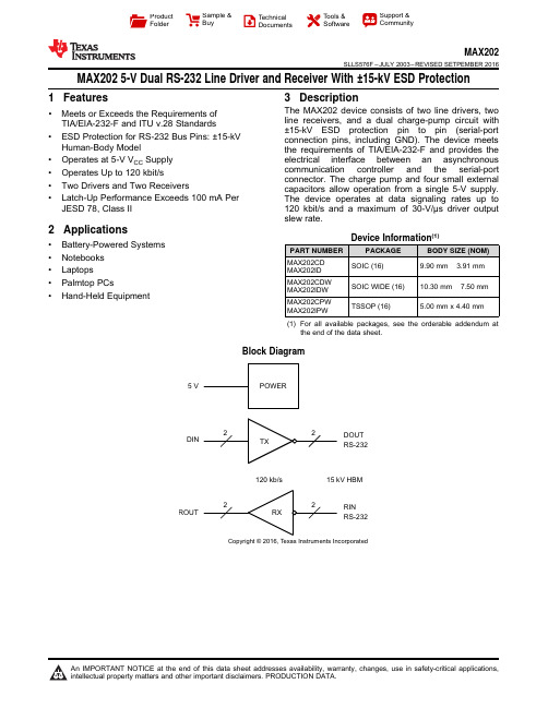
5 V DINROUTDOUT RS-232RIN RS-232120 kb/s15 kV HBMCopyright © 2016,Texas Instruments IncorporatedProduct FolderSample &BuyTechnical Documents Tools &SoftwareSupport &CommunityAn IMPORTANT NOTICE at the end of this data sheet addresses availability,warranty,changes,use in safety-critical applications,intellectual property matters and other important disclaimers.PRODUCTION DATA.MAX202SLLS576F –JULY 2003–REVISED SETPEMBER 2016MAX2025-V Dual RS-232Line Driver and Receiver With ±15-kV ESD Protection1Features•Meets or Exceeds the Requirements of TIA/EIA-232-F and ITU v.28Standards•ESD Protection for RS-232Bus Pins:±15-kV Human-Body Model•Operates at 5-V V CC Supply •Operates Up to 120kbit/s•Two Drivers and Two Receivers•Latch-Up Performance Exceeds 100mA Per JESD 78,Class II2Applications•Battery-Powered Systems •Notebooks •Laptops•Palmtop PCs•Hand-Held Equipment3DescriptionThe MAX202device consists of two line drivers,two line receivers,and a dual charge-pump circuit with ±15-kV ESD protection pin to pin (serial-port connection pins,including GND).The device meets the requirements of TIA/EIA-232-F and provides the electrical interface between an asynchronous communication controller and the serial-port connector.The charge pump and four small external capacitors allow operation from a single 5-V supply.The device operates at data signaling rates up to 120kbit/s and a maximum of 30-V/µs driver output slew rate.Device Information (1)PART NUMBER PACKAGE BODY SIZE (NOM)MAX202CD MAX202ID SOIC (16)9.90mm ×3.91mm MAX202CDW MAX202IDW SOIC WIDE (16)10.30mm ×7.50mm MAX202CPW MAX202IPWTSSOP (16)5.00mm x 4.40mm(1)For all available packages,see the orderable addendum atthe end of the data sheet.Block Diagram2MAX202SLLS576F –JULY 2003–REVISED SETPEMBER 2016Product Folder Links:MAX202Submit Documentation FeedbackCopyright ©2003–2016,Texas Instruments IncorporatedTable of Contents1Features ..................................................................12Applications ...........................................................13Description .............................................................14Revision History .....................................................25Pin Configuration and Functions . (36)Specifications .........................................................46.1Absolute Maximum Ratings......................................46.2ESD Ratings..............................................................46.3Recommended Operating Conditions.......................46.4Thermal Information..................................................46.5Electrical Characteristics...........................................56.6Switching Characteristics..........................................56.7Typical Characteristics .............................................67Parameter Measurement Information ..................78Detailed Description . (8)8.1Overview...................................................................88.2Functional Block Diagram.. (8)8.3Feature Description...................................................88.4Device Functional Modes (8)9Application and Implementation (10)9.1Application Information............................................109.2Typical Application.. (10)10Power Supply Recommendations .....................1311Layout . (13)11.1Layout Guidelines ................................................1311.2Layout Example. (13)12Device and Documentation Support (14)12.1Receiving Notification of Documentation Updates 1412.2Community Resources..........................................1412.3Trademarks...........................................................1412.4Electrostatic Discharge Caution............................1412.5Glossary................................................................1413Mechanical,Packaging,and OrderableInformation (14)4Revision HistoryNOTE:Page numbers for previous revisions may differ from page numbers in the current version.Changes from Revision E (April 2007)to Revision F Page•Added ESD Ratings table,Feature Description section,Device Functional Modes ,Application and Implementation section,Power Supply Recommendations section,Layout section,Device and Documentation Support section,andMechanical,Packaging,and Orderable Information section..................................................................................................1•Removed the Ordering Information table;see POA at the end of the data sheet .................................................................1•Changed values in the Thermal Information table to align with JEDEC standards (4)C1+ V CC V+ GND C1± DOUT1C2+ RIN1C2± ROUT1V ± DIN1DOUT2 DIN2RIN2ROUT23MAX202SLLS576F –JULY 2003–REVISED SETPEMBER 2016Product Folder Links:MAX202Submit Documentation FeedbackCopyright ©2003–2016,Texas Instruments Incorporated 5Pin Configuration and FunctionsD,DW,or PW Package 16-Pin SOIC or TSSOPTop ViewPin FunctionsPINI/O DESCRIPTION 1C1+—Positive lead of C1capacitor2V+O Positive charge pump output for storage capacitor only 3C1–—Negative lead of C1capacitor 4C2+—Positive lead of C2capacitor 5C2–—Negative lead of C2capacitor6V–O Negative charge pump output for storage capacitor only 7DOUT2O RS-232line data output (to remote RS-232system)8RIN2I RS-232line data input (from remote RS-232system)9ROUT2O Logic data output (to UART)10DIN2I Logic data input (from UART)11DIN1I Logic data input (from UART)12ROUT1O Logic data output (to UART)13RIN1I RS-232line data input (from remote RS-232system)14DOUT1O RS-232line data output (to remote RS-232system)15GND —Ground16V CC—Supply voltage,connect to external 5-V power supply4MAX202SLLS576F –JULY 2003–REVISED SETPEMBER 2016Product Folder Links:MAX202Submit Documentation FeedbackCopyright ©2003–2016,Texas Instruments Incorporated(1)Stresses beyond those listed under Absolute Maximum Ratings may cause permanent damage to the device.These are stress ratings only,which do not imply functional operation of the device at these or any other conditions beyond those indicated under Recommended Operating Conditions .Exposure to absolute-maximum-rated conditions for extended periods may affect device reliability.(2)All voltages are with respect to network GND.6Specifications6.1Absolute Maximum Ratingsover operating free-air temperature range (unless otherwise noted)(1)MINMAX UNIT Supply voltage,V CC (2)–0.36V Positive charge pump voltage,V+(2)V CC –0.314V Negative charge pump voltage,V–(2)–140.3V Input voltage,V I Drivers –0.3V++0.3V Receivers ±30Output voltage,V ODrivers V––0.3V++0.3VReceivers–0.3V CC +0.3Short-circuit duration,D OUTContinuousOperating junction temperature,T J 150°C Storage temperature,T stg –65150°C (1)JEDEC document JEP155states that 500-V HBM allows safe manufacturing with a standard ESD control process.(2)JEDEC document JEP157states that 250-V CDM allows safe manufacturing with a standard ESD control process.6.2ESD RatingsVALUEUNITV (ESD)Electrostatic dischargeHuman-body model (HBM),per ANSI/ESDA/JEDEC JS-001(1)Pins 7,8,13,and 14±15000V All other pins±2000Charged-device model (CDM),per JEDEC specification JESD22-C101(2)±1500(1)Test conditions are C1–C4=0.1µF at V CC =5V ±0.5V.6.3Recommended Operating Conditionsover operating free-air temperature range (unless otherwise noted (1);see Figure 10)MINNOMMAX UNIT Supply voltage4.555.5V V IH Driver high-level input voltage (D IN )2V V IL Driver low-level input voltage (D IN )0.8V V I Driver input voltage (D IN )0 5.5V Receiver input voltage –3030T A Operating free-air temperatureMAX202C 070°CMAX202I–4085(1)For more information about traditional and new thermal metrics,see the Semiconductor and IC Package Thermal Metrics application report.6.4Thermal InformationTHERMAL METRIC (1)MAX202UNITD (SOIC)DW (SOIC)PW (TSSOP)16PINS 16PINS 16PINS R θJA Junction-to-ambient thermal resistance 76.276.8101°C/W R θJC(top)Junction-to-case (top)thermal resistance 36.839.636.4°C/W R θJB Junction-to-board thermal resistance 33.941.545.9°C/W ψJT Junction-to-top characterization parameter 6.712.6 2.7°C/W ψJB Junction-to-board characterization parameter33.640.945.3°C/W5MAX202SLLS576F –JULY 2003–REVISED SETPEMBER 2016Product Folder Links:MAX202Submit Documentation FeedbackCopyright ©2003–2016,Texas Instruments Incorporated (1)Test conditions are C1–C4=0.1µF at V CC =5V ±0.5V.(2)All typical values are at V CC =5V,and T A =25°C.(3)Short-circuit durations should be controlled to prevent exceeding the device absolute power-dissipation ratings,and not more than one output should be shorted at a time.6.5Electrical Characteristicsover recommended ranges of supply voltage and operating free-air temperature (unless otherwise noted;see Figure 10)(1)PARAMETERTEST CONDITIONSMINTYP (2)MAX UNIT I CC Supply currentNo load,V CC =5V815mADRIVER SECTIONV OH High-level output voltage D OUT at R L =3k Ωto GND,D IN =GND 59V V OL Low-level output voltage D OUT at R L =3k Ωto GND,D IN =V CC –5–9V I IH High-level input current V I =V CC 0200µA I IL Low-level input current V I at 0V0–200µA I OS (3)Short-circuit output current V CC =5.5V,V O =0V±10±60mA r O Output resistance V CC ,V+,and V–=0V,V O =±2V 300ΩRECEIVER SECTIONV OH High-level output voltage I OH =–1mA 3.5V CC –0.4V V OL Low-level output voltageI OL =1.6mA 0.4V V IT+Positive-going input threshold voltage V CC =5V,T A =25°C 1.7 2.4V V IT–Negative-going input threshold voltage V CC =5V,T A =25°C0.8 1.2V V hys Input hysteresis (V IT+–V IT–)0.20.51V r i Input resistanceV I =±3V to ±25V357k Ω(1)Test conditions are C1–C4=0.1µF at V CC =5V ±0.5V.(2)All typical values are at V CC =5V,and T A =25°C.(3)Pulse skew is defined as |t PLH –t PHL |of each channel of the same device.6.6Switching Characteristicsover recommended ranges of suply voltage and operating free-air temperature (unless otherwise noted;see Figure 10)(1)PARAMETERTEST CONDITIONSMINTYP (2)MAXUNITDRIVER SECTIONMaximum data rateC L =50pF to 1000pF,R L =3k Ωto 7k ΩoneD OUT switching,see Figure 6120kbit/s t PLH(D)Propagation delay time,low-to high-level output C L =2500pF,R L =3k Ω,all drivers loaded,see Figure 62µs t PHL(D)Propagation delay time,high-to low-level output C L =2500pF,R L =3k Ω,all drivers loaded,see Figure 62µs t sk(p)Pulse skew (3)C L =150to 2500pF,R L =3k Ωto 7k Ω,see Figure 7300ns SR(tr)Slew rate,transition regionC L =50to 1000pF,R L =3k Ωto 7k Ω,V CC =5V,see Figure 63630V/µsRECEIVER SECTION (SEE Figure 8)t PLH(R)Propagation delay time,low-to high-level output C L =150pF 0.510µs t PHL(R)Propagation delay time,high-to low-level output C L =150pF 0.510µs t sk(p)Pulse skew (3)C L =150pF300ns6MAX202SLLS576F –JULY 2003–REVISED SETPEMBER 2016Product Folder Links:MAX202Submit Documentation FeedbackCopyright ©2003–2016,Texas Instruments Incorporated6.7Typical Characteristicsat T A =25°C (unless otherwise noted)TEST CIRCUITVOLTAGE WAVEFORMS50%50%–3 V3 V1.5 V1.5 VOutputInputV OL V OHt PHL (R)t PLH (R)OutputA)TEST CIRCUITVOLTAGE WAVEFORMS0 V 3 VOutputInputV OLV OHt PLH (D)t PHL (D)50%50%1.5 V1.5 VRS-232OutputA)TEST CIRCUITVOLTAGE WAVEFORMS0 V3 VOutputInputV OLV OH t PLH (D)RS-232Outputt PHL (D)A)1.5 V1.5 V3 V –3 V3 V –3 VSR(tf) =6 Vt or t PHL(D PLH(D))7MAX202SLLS576F –JULY 2003–REVISED SETPEMBER 2016Product Folder Links:MAX202Submit Documentation FeedbackCopyright ©2003–2016,Texas Instruments Incorporated 7Parameter Measurement InformationA.C L includes probe and jig capacitance.B.The pulse generator has the following characteristics:PRR =120kbit/s,Z O =50Ω,50%duty cycle,t r ≤10ns,t f ≤10ns.Figure 6.Driver Slew RateA.C L includes probe and jig capacitance.B.The pulse generator has the following characteristics:PRR =120kbit/s,Z O =50Ω,50%duty cycle,t r ≤10ns,t f ≤10ns.Figure 7.Driver Pulse SkewA.C L includes probe and jig capacitance.B.The pulse generator has the following characteristics:Z O =50Ω,50%duty cycle,t r ≤10ns,t f ≤10ns.Figure 8.Receiver Propagation Delay Times5 V DINROUTDOUT RS-232RIN RS-232120 kb/s15 kV HBMCopyright © 2016,Texas Instruments Incorporated8MAX202SLLS576F –JULY 2003–REVISED SETPEMBER 2016Product Folder Links:MAX202Submit Documentation FeedbackCopyright ©2003–2016,Texas Instruments Incorporated8Detailed Description8.1OverviewThe MAX202device is a dual driver and receiver that includes a capacitive voltage generator using four capacitors to supply TIA/EIA-232-F voltage levels from a single 5-V supply.Each receiver converts TIA/EIA-232-F inputs to 5-V TTL/CMOS levels.These receivers have shorted and open fail safe.The receiver can accept up to ±30-V inputs and decode inputs as low as ±3V.Each driver converts TTL/CMOS input levels into TIA/EIA-232-F levels.Outputs are protected against shorts to ground.8.2Functional Block Diagram8.3Feature Description8.3.1PowerThe power block increases and inverts the 5-V supply for the RS-232driver using a charge pump that requires four 0.1-µF external capacitors.8.3.2RS-232DriverTwo drivers interface standard logic levels to RS-232levels.The driver inputs do not have internal pullup resistors.Do not float the driver inputs.8.3.3RS-232ReceiverTwo Schmitt trigger receivers interface RS-232levels to standard logic levels.Each receiver has an internal 5-k Ωload to ground.An open input results in a high output on ROUT.8.4Device Functional Modes8.4.1V CC Powered by 5-VThe device is in normal operation when powered by 5V.8.4.2V CC UnpoweredWhen MAX202is unpowered,it can be safely connected to an active remote RS-232device.DIN1DOUT1RIN1ROUT1DIN2DOUT2RIN2ROUT29MAX202SLLS576F –JULY 2003–REVISED SETPEMBER 2016Product Folder Links:MAX202Submit Documentation FeedbackCopyright ©2003–2016,Texas Instruments Incorporated Device Functional Modes (continued)8.4.3Truth TablesTable 1and Table 2list the function for each driver and receiver (respectively).(1)H =high level,L =low levelTable 1.Function Table forEach Driver (1)INPUT DIN OUTPUT DOUTL H HL(1)H =high level,L =low level,Open =input disconnected or connected driver offTable 2.Function Table forEach Receiver (1)INPUT RIN OUTPUT ROUTL H H L OpenHFigure 9.Logic Diagram (Positive Logic)CBYPASS = 0.1F,m C10.1F,m 6.3 VCopyright © 2016,Texas Instruments Incorporated10MAX202SLLS576F –JULY 2003–REVISED SETPEMBER 2016Product Folder Links:MAX202Submit Documentation FeedbackCopyright ©2003–2016,Texas Instruments Incorporated9Application and ImplementationNOTEInformation in the following applications sections is not part of the TI component specification,and TI does not warrant its accuracy or completeness.TI’s customers are responsible for determining suitability of components for their purposes.Customers should validate and test their design implementation to confirm system functionality.9.1Application InformationFor proper operation,add capacitors as shown in Figure 10.Pins 9through 12connect to UART or general purpose logic lines.RS-232lines on pins 7,8,13,and 14connect to a connector or cable.9.2Typical ApplicationA.C3can be connected to V CC or GND.B.Resistor values shown are nominal.C.Nonpolarized ceramic capacitors are acceptable.If polarized tantalum or electrolytic capacitors are used,they must be connected as shown.Figure 10.Typical Operating Circuit and Capacitor Values9.2.1Design Requirements •V CC minimum is 4.5V and maximum is 5.5V.•Maximum recommended bit rate is 120kbps.RVHBM MAX202 SLLS576F–JULY2003–REVISED SETPEMBER2016 Typical Application(continued)9.2.2Detailed Design Procedure9.2.2.1Capacitor SelectionThe capacitor type used for C1through C4is not critical for proper operation.The MAX202requires0.1-µF capacitors.Capacitors up to10µF can be used without harm.Ceramic dielectrics are suggested for the0.1-µF capacitors.When using the minimum recommended capacitor values,make sure the capacitance value does not degrade excessively as the operating temperature varies.If in doubt,use capacitors with a larger(for example, 2×)nominal value.The capacitors'effective series resistance(ESR),which usually rises at low temperatures, influences the amount of ripple on V+and V–.Use larger capacitors(up to10µF)to reduce the output impedance at V+and V–.Bypass V CC to ground with at least0.1µF.In applications sensitive to power-supply noise generated by the charge pumps,decouple V CC to ground with a capacitor the same size as(or larger than)the charge-pump capacitors(C1to C4).9.2.2.2ESD ProtectionMAX202devices have standard ESD protection structures incorporated on all pins to protect against electrostatic discharges encountered during assembly and handling.In addition,the RS-232bus pins(driver outputs and receiver inputs)of these devices have an extra level of ESD protection.Advanced ESD structures were designed to successfully protect these bus pins against ESD discharge of±15-kV when powered down.9.2.2.3ESD Test ConditionsStringent ESD testing is performed by TI based on various conditions and procedures.Please contact TI for a reliability report that documents test setup,methodology,and results.9.2.2.4Human-Body Model(HBM)The HBM of ESD testing is shown in Figure11.Figure12shows the current waveform that is generated during a discharge into a low impedance.The model consists of a100-pF capacitor,charged to the ESD voltage of concern,and subsequently discharged into the device under test(DUT)through a1.5-kΩresistor.Figure11.HBM ESD Test Circuit1001502005001.51.00.50.0I -AD U T MAX202SLLS576F –JULY 2003–REVISED SETPEMBER Typical Application (continued)Figure 12.Typical HBM Current Waveform9.2.3Application Curve120kbit/s,1-nF loadFigure 13.Driver and Receiver Loopback SignalMAX202 SLLS576F–JULY2003–REVISED SETPEMBER201610Power Supply RecommendationsThe V CC voltage must be connected to the same power source used for logic device connected to DIN and ROUT pins.V CC must be between4.5V and5.5V.11Layout11.1Layout GuidelinesKeep the external capacitor traces short.This is more important on C1and C2nodes that have the fastest rise and fall times.For best ESD performance,make the impedance from MAX202ground pin to the ground plane of the circuit board as low as e wide metal and multiple vias on both sides of ground pin.11.2Layout ExampleFigure14.MAX202Circuit Board LayoutMAX202SLLS576F–JULY2003–REVISED 12Device and Documentation Support12.1Receiving Notification of Documentation UpdatesTo receive notification of documentation updates,navigate to the device product folder on .In the upper right corner,click on Alert me to register and receive a weekly digest of any product information that has changed.For change details,review the revision history included in any revised document.12.2Community ResourcesThe following links connect to TI community resources.Linked contents are provided"AS IS"by the respective contributors.They do not constitute TI specifications and do not necessarily reflect TI's views;see TI's Terms of Use.TI E2E™Online Community TI's Engineer-to-Engineer(E2E)Community.Created to foster collaboration among engineers.At ,you can ask questions,share knowledge,explore ideas and helpsolve problems with fellow engineers.Design Support TI's Design Support Quickly find helpful E2E forums along with design support tools and contact information for technical support.12.3TrademarksE2E is a trademark of Texas Instruments.All other trademarks are the property of their respective owners.12.4Electrostatic Discharge CautionThese devices have limited built-in ESD protection.The leads should be shorted together or the device placed in conductive foam during storage or handling to prevent electrostatic damage to the MOS gates.12.5GlossarySLYZ022—TI Glossary.This glossary lists and explains terms,acronyms,and definitions.13Mechanical,Packaging,and Orderable InformationThe following pages include mechanical,packaging,and orderable information.This information is the most current data available for the designated devices.This data is subject to change without notice and revision of this document.For browser-based versions of this data sheet,refer to the left-hand navigation.PACKAGING INFORMATIONAddendum-Page 1(1) The marketing status values are defined as follows:ACTIVE: Product device recommended for new designs.LIFEBUY: TI has announced that the device will be discontinued, and a lifetime-buy period is in effect.NRND: Not recommended for new designs. Device is in production to support existing customers, but TI does not recommend using this part in a new design.PREVIEW: Device has been announced but is not in production. Samples may or may not be available.OBSOLETE: TI has discontinued the production of the device.(2) Eco Plan - The planned eco-friendly classification: Pb-Free (RoHS), Pb-Free (RoHS Exempt), or Green (RoHS & no Sb/Br) - please check /productcontent for the latest availability information and additional product content details.TBD: The Pb-Free/Green conversion plan has not been defined.Pb-Free (RoHS): TI's terms "Lead-Free" or "Pb-Free" mean semiconductor products that are compatible with the current RoHS requirements for all 6 substances, including the requirement that lead not exceed 0.1% by weight in homogeneous materials. Where designed to be soldered at high temperatures, TI Pb-Free products are suitable for use in specified lead-free processes.Pb-Free (RoHS Exempt): This component has a RoHS exemption for either 1) lead-based flip-chip solder bumps used between the die and package, or 2) lead-based die adhesive used between the die and leadframe. The component is otherwise considered Pb-Free (RoHS compatible) as defined above.Green (RoHS & no Sb/Br): TI defines "Green" to mean Pb-Free (RoHS compatible), and free of Bromine (Br) and Antimony (Sb) based flame retardants (Br or Sb do not exceed 0.1% by weight in homogeneous material)(3) MSL, Peak Temp. - The Moisture Sensitivity Level rating according to the JEDEC industry standard classifications, and peak solder temperature.(4) There may be additional marking, which relates to the logo, the lot trace code information, or the environmental category on the device.Addendum-Page 2(5) Multiple Device Markings will be inside parentheses. Only one Device Marking contained in parentheses and separated by a "~" will appear on a device. If a line is indented then it is a continuation of the previous line and the two combined represent the entire Device Marking for that device.(6) Lead/Ball Finish - Orderable Devices may have multiple material finish options. Finish options are separated by a vertical ruled line. Lead/Ball Finish values may wrap to two lines if the finish value exceeds the maximum column width.Important Information and Disclaimer:The information provided on this page represents TI's knowledge and belief as of the date that it is provided. TI bases its knowledge and belief on information provided by third parties, and makes no representation or warranty as to the accuracy of such information. Efforts are underway to better integrate information from third parties. TI has taken and continues to take reasonable steps to provide representative and accurate information but may not have conducted destructive testing or chemical analysis on incoming materials and chemicals. TI and TI suppliers consider certain information to be proprietary, and thus CAS numbers and other limited information may not be available for release.In no event shall TI's liability arising out of such information exceed the total purchase price of the TI part(s) at issue in this document sold by TI to Customer on an annual basis.Addendum-Page 3TAPE AND REEL INFORMATION*All dimensions are nominal Device Package Type Package DrawingPinsSPQ Reel Diameter (mm)Reel Width W1(mm)A0(mm)B0(mm)K0(mm)P1(mm)W (mm)Pin1Quadrant MAX202CDR SOICD 162500330.016.4 6.510.3 2.18.016.0Q1MAX202CDWR SOICDW 162000330.016.410.7510.7 2.712.016.0Q1MAX202CPWR TSSOPPW 162000330.012.4 6.9 5.6 1.68.012.0Q1MAX202IDR SOICD 162500330.016.4 6.510.3 2.18.016.0Q1MAX202IDWR SOICDW 162000330.016.410.7510.7 2.712.016.0Q1MAX202IPWR TSSOP PW 162000330.012.4 6.9 5.6 1.68.012.0Q1*All dimensions are nominalDevice Package Type Package Drawing Pins SPQ Length(mm)Width(mm)Height(mm) MAX202CDR SOIC D162500333.2345.928.6 MAX202CDWR SOIC DW162000367.0367.038.0 MAX202CPWR TSSOP PW162000367.0367.035.0 MAX202IDR SOIC D162500333.2345.928.6 MAX202IDWR SOIC DW162000367.0367.038.0MAX202IPWR TSSOP PW162000367.0367.035.0IMPORTANT NOTICETexas Instruments Incorporated and its subsidiaries(TI)reserve the right to make corrections,enhancements,improvements and other changes to its semiconductor products and services per JESD46,latest issue,and to discontinue any product or service per JESD48,latest issue.Buyers should obtain the latest relevant information before placing orders and should verify that such information is current and complete.All semiconductor products(also referred to herein as“components”)are sold subject to TI’s terms and conditions of sale supplied at the time of order acknowledgment.TI warrants performance of its components to the specifications applicable at the time of sale,in accordance with the warranty in TI’s terms and conditions of sale of semiconductor products.Testing and other quality control techniques are used to the extent TI deems necessary to support this warranty.Except where mandated by applicable law,testing of all parameters of each component is not necessarily performed.TI assumes no liability for applications assistance or the design of Buyers’products.Buyers are responsible for their products and applications using TI components.To minimize the risks associated with Buyers’products and applications,Buyers should provide adequate design and operating safeguards.TI does not warrant or represent that any license,either express or implied,is granted under any patent right,copyright,mask work right,or other intellectual property right relating to any combination,machine,or process in which TI components or services are rmation published by TI regarding third-party products or services does not constitute a license to use such products or services or a warranty or endorsement e of such information may require a license from a third party under the patents or other intellectual property of the third party,or a license from TI under the patents or other intellectual property of TI.Reproduction of significant portions of TI information in TI data books or data sheets is permissible only if reproduction is without alteration and is accompanied by all associated warranties,conditions,limitations,and notices.TI is not responsible or liable for such altered rmation of third parties may be subject to additional restrictions.Resale of TI components or services with statements different from or beyond the parameters stated by TI for that component or service voids all express and any implied warranties for the associated TI component or service and is an unfair and deceptive business practice. TI is not responsible or liable for any such statements.Buyer acknowledges and agrees that it is solely responsible for compliance with all legal,regulatory and safety-related requirements concerning its products,and any use of TI components in its applications,notwithstanding any applications-related information or support that may be provided by TI.Buyer represents and agrees that it has all the necessary expertise to create and implement safeguards which anticipate dangerous consequences of failures,monitor failures and their consequences,lessen the likelihood of failures that might cause harm and take appropriate remedial actions.Buyer will fully indemnify TI and its representatives against any damages arising out of the use of any TI components in safety-critical applications.In some cases,TI components may be promoted specifically to facilitate safety-related applications.With such components,TI’s goal is to help enable customers to design and create their own end-product solutions that meet applicable functional safety standards and requirements.Nonetheless,such components are subject to these terms.No TI components are authorized for use in FDA Class III(or similar life-critical medical equipment)unless authorized officers of the parties have executed a special agreement specifically governing such use.Only those TI components which TI has specifically designated as military grade or“enhanced plastic”are designed and intended for use in military/aerospace applications or environments.Buyer acknowledges and agrees that any military or aerospace use of TI components which have not been so designated is solely at the Buyer's risk,and that Buyer is solely responsible for compliance with all legal and regulatory requirements in connection with such use.TI has specifically designated certain components as meeting ISO/TS16949requirements,mainly for automotive use.In any case of use of non-designated products,TI will not be responsible for any failure to meet ISO/TS16949.Products ApplicationsAudio /audio Automotive and Transportation /automotiveAmplifiers Communications and Telecom /communicationsData Converters Computers and Peripherals /computersDLP®Products Consumer Electronics /consumer-appsDSP Energy and Lighting /energyClocks and Timers /clocks Industrial /industrialInterface Medical /medicalLogic Security /securityPower Mgmt Space,Avionics and Defense /space-avionics-defense Microcontrollers Video and Imaging /videoRFID OMAP Applications Processors /omap TI E2E Community Wireless Connectivity /wirelessconnectivityMailing Address:Texas Instruments,Post Office Box655303,Dallas,Texas75265Copyright©2016,Texas Instruments Incorporated。
MAX31865中文资料_数据手册_参数

VIL
CS, SDI, SCLK
Input Logic 1
Analog Voltages (FORCE+,FORCE2, FORCE-, RTDIN+, RTDIN-) Reference Resistor Cable Resistance
VIH
CS, SDI, SCLK
Normal conversion results
MAX31865 RTD-to-Digital Converter
ABSOLUTE MAXIMUM RATINGS
Voltage Range on VDD Relative to GND1.............-0.3V to +4.0V Voltage Range on BIAS, REFIN+,
Applications
Industrial Equipment Medical Equipment Instrumentation
Ordering Information appears at end of data sheet.
For related parts and recommended products to use with this part, refer to /MAX31865.related.
PACKAGE THERMAL CHARACTERISTICS (Note 1)
TQFN Junction-to-Ambient Thermal Resistance (qJA)...........29°C/W Junction-to-Case Thermal Resistance (qJC)..................2°C/W
EVALUATION KIT AVAILABLE
稳压模块
EZELAND 输入特性输入电压范围(lnput voltage range) 4.75VDC-5.25VDC 11.40VDC-12.60VDC 14.25VDC-15.75VDC 22.80VDC-25.20VDC 45.60VDC-50.40VDC输出特性输出电压精度(voltage accuracy) 标称输出电压±3%负载效应(Load regulation) 0%至100%负载变化时±1.0%(最大值)源效应(Line regulation) 输入电压从低端至高端变化时±1.0%(最大值) 纹波及噪声(Ripple and noise) 50mVpk-pk(最大值)温度系数(Temperature coefficient) ±0.10%/℃(最大值)一般特性效率(Efficiency)见产品选型表隔离电压(lsolation voltage) 输入至输出(1分钟漏电流<0. 5mA)500VDC开关频率(Switching frequency)150KHz最小无故障间隔时间(MTBF) 200000小时环境特性工作温度(Operatlng ambient)-25℃至+85℃最大壳温(Max Case temperature)+90℃存储温度(Storage temperature)-40℃至+120℃相对湿度(Relative density)10%至90%SR01系列产品型号输入电压范围(V)标称输出电压(V)标称输出电流(mA )纹波及噪声(mVp-p) 典型效应(%) V out1 V out2 lout1 lout2 out1 out2SR5S5/100A 4.75-5.25 5 100 50 40 SR5S12/100A 4.75-5.25 12 100 50 52 SR5S15/100A 4.75-5.25 15 100 50 52 SR5S24/50A 4.75-5.25 24 50 50 52 SR12S5/100A 11.40-12.60 5 100 50 40 SR12S12/100A 11.40-12.60 12 100 50 52 SR12S15/100A 11.40-12.60 15 100 50 52SR12S24/50A 11.40-12.60 24 50 50 52 SR15S5/100A 14.25-15.75 5 100 50 40 SR15S12/100A 14.25-15.75 12 100 50 52 SR15S15/100A 14.25-15.75 15 100 50 52 SR15S24/50A 14.25-15.75 24 50 50 52 SR24S5/100A 22.80-25.20 5 100 50 40 SR24S12/100A 22.80-25.20 12 100 50 52 SR24S15/100A 22.80-25.20 15 100 50 52 SR24S24/50A 22.80-25.20 24 50 50 52 SR5D5/100A 4.75-5.25 +5 -5 100 100 50 50 45 SR5D12/50A 4.75-5.25 +12 -12 50 50 50 50 52 SR5D15/50A 4.75-5.25 +15 -15 50 50 50 50 52 SR5D24/20A 4.75-5.25 +24 -24 20 20 50 50 52 SR12D5/100A 11.40-12.60 +5 -5 100 100 50 50 45 SR12D12/50A 11.40-12.60 +12 -12 50 50 50 50 52 SR12D15/50A 11.40-12.60 +15 -15 50 50 50 50 52 SR12D24/20A 11.40-12.60 +24 -24 20 20 50 50 52 SR15D5/100A 14.25-15.75 +5 -5 100 100 50 50 45 SR15D12/50A 14.25-15.75 +12 -12 50 50 50 50 52 SR15D15/50A 14.25-15.75 +15 -15 50 50 50 50 52 SR15D24/20A 14.25-15.75 +24 -24 20 20 50 50 52 SR24D5/100A 22.80-25.20 +5 -5 100 100 50 50 45 SR24D12/50A 22.80-25.20 +12 -12 50 50 50 50 52 SR24D15/50A 22.80-25.20 +15 -15 50 50 50 50 52 SR24D24/20A 22.80-25.20 +24 -24 20 20 50 50 52SR03系列产品型号输入电压范围(V)标称输出电压(V)标称输出电流(mA)纹波及噪声(mVp-p)典型效应(%) V out1 V out2 V out3 lout1 lout2 lout3 out1 out2 out3SR5S5/200A 4-75-5.25 5 200 50 40 SR5S5/200B 4.75-5.25 5 200 50 50 SR5S5/500B 4.75-5.25 5 500 50 55SR5S12/250B 4.75-5.25 12 250 50 60 SR5S15/200B 4.75-5.25 15 200 50 60 SR5S24/125B 4.75-5.25 24 125 50 60 SR12S5/200A 11.40-12.60 5 200 50 40 SR12S5/500B 11.40-12.60 5 500 50 55 SR12S12/250B 11.40-12.60 12 250 50 60 SR12S15/200B 11.40-12.60 15 200 50 60 SR12S24/125B 11.40-12.60 24 125 50 60 SR24S5/200A 22.80-25.20 5 200 50 40 SR24S5/500B 22.80-25.20 5 500 50 55 SR24S12/250B 22.80-25.20 12 250 50 60 SR24S15/200B 22.80-25.20 15 200 50 60 SR24S24/125B 22.80-25.20 24 125 50 60 SR48S5/500B 45.60-50.40 5 500 50 55 SR48S12/250B 45.60-50.40 12 250 50 60 SR48S15/200B 45.60-50.40 15 200 50 60 SR48S24/125B 45.60-50.40 24 125 50 60 SR5D12/100A 4.75-5.25 +12 -12 100 100 50 50 52 SR5D12/100B 4.75-5.25 +12 -12 100 100 50 50 60 SR5D15/100A 4.75-5.25 +15 -15 100 100 50 50 52 SR5D15/100B 4.75-5.25 +15 -15 100 100 50 50 60 SR5D24/60B 4.75-5.25 +24 -24 60 60 50 50 60 SR12D12/100A 11.40-12.60 +12 -12 100 100 50 50 52 SR12D12/100B 11.40-12.60 +12 -12 100 100 50 50 60 SR12D15/100A 11.40-12.60 +15 -15 100 100 50 50 52 SR12D15/100B 11.40-12.60 +15 -15 100 100 50 50 60 SR12D24/60B 11.40-12.60 +24 -24 60 60 50 50 60 SR15D12/100A 14.25-15.75 +12 -12 100 100 50 50 52 SR15D15/100A 14.25-15.75 +15 -15 100 100 50 50 52 SR24D12/100A 22.80-25.20 +12 -12 100 100 50 50 52 SR24D12/100B 22.80-25.20 +12 -12 100 100 50 50 60 SR24D15/100A 22.80-25.20 +15 -15 100 100 50 50 52 SR24D15/100B 22.80-25.20 +15 -15 100 100 50 50 60SR24D24/60B 22.80-25.20 +24 -24 60 60 50 50 60 SR48D12/100B 45.60-50.40 +12 -12 100 100 50 50 60 SR48D15/100B 45.60-50.40 +15 -15 100 100 50 50 60 SR48D24/60B 45.60-50.40 +24 -24 60 60 50 50 60 SR5D12S5B 4.75-5.25 +12 -12 +5 100 100 100 50 50 50 64 SR5D15S5B 4.75-5.25 +15 -15 +5 100 100 100 50 50 50 64 SR12D12S5B 11.40-12.60 +12 -12 +5 100 100 100 50 50 50 64 SR12D15S5B 11.40-12.60 +15 -15 +5 100 100 100 50 50 50 64 SR24D12S5B 22.80-25.20 +12 -12 +5 100 100 100 50 50 50 64 SR24D15S5B 22.80-25.20 +15 -15 +5 100 100 100 50 50 50 64SR05系列产品型号输入电压范围(V)标称输出电压(mA)标称输出电流(mA)纹波及噪声(mVp-p)典型效应(%) V out1 V out2 lout1 lout2 out1 out2SR5S5/1000B 4.75-5.25 5 1000 50 65 SR5S5/1000C 4.75-5.25 5 1000 50 60 SR5S12/400C 4.75-5.25 12 400 50 64 SR5S15/300C 4.75-5.25 15 300 50 64 SR5S24/200C 4.75-5.25 24 200 50 64 SR12S5/1000B 11.40-12.60 5 1000 50 65 SR12S5/1000C 11.40-12.60 5 1000 50 60 SR12S12/400C 11.40-12.60 12 400 50 64 SR12S15/300C 11.40-12.60 15 300 50 64 SR12S24/200C 11.40-12.60 24 200 50 64 SR24S5/1000B 22.80-25.20 5 1000 50 65 SR24S5/1000C 22.80-25.20 5 1000 50 60 SR24S12/400C 22.80-25.20 12 400 50 64 SR24S15/300C 22.80-25.20 15 300 50 64 SR24S24/200C 22.80-25.20 24 200 50 64 SR48S5/1000C 45.60-50.40 5 1000 50 60 SR48S12/400C 45.60-50.40 12 400 50 64 SR48S15/300C 45.60-50.40 15 300 50 64 SR48S24/200C 45.60-50.40 24 200 50 64 SR5D5/500C 4.75-5.25 +5 -5 500 500 50 50 60SR5D12/150C 4.75-5.25 +12 -12 150 150 50 50 64 SR5D15/150C 4.75-5.25 +15 -15 150 150 50 50 64 SR5D24/100C 4.75-5.25 +24 -24 100 100 50 50 64 SR12D5/500C 11.40-12.60 +5 -5 500 500 50 50 60 SR12D12/150C 11.40-12.60 +12 -12 150 150 50 50 64 SR12D15/150C 11.40-12.60 +15 -15 150 150 50 50 64 SR12D24/100C 11.40-12.60 +24 -24 100 100 50 50 64 SR24D5/500C 22.80-25.20 +5 -5 500 500 50 50 60 SR24D12/150C 22.80-25.20 +12 -12 150 150 50 50 64 SR24D15/150C 22.80-25.20 +15 -15 150 150 50 50 64 SR24D24/100C 22.80-25.20 +24 -24 100 100 50 50 64 SR48D5/500C 45.60-50.40 +5 -5 500 500 50 50 60 SR48D12/150C 45.60-50.40 +12 -12 150 150 50 50 64 SR48D15/150C 45.60-50.40 +15 -15 150 150 50 50 64 SR48D24/100C 45.60-50.40 +24 -24 100 100 50 50 64模块电源用途:电力、医疗、通讯、电子仪器仪表、电力、自动化、智能楼宇、安防、电力机车、继电保护等天津泽沥电子。
电磁兼容(EMC)设计参考电路
1000pF/2KV FBMA-11-160808-601A10T
1 2 3.3V-Earth
L5
1000pF
C5
C6
1000pF
C1 1000pF
L3
C4 100nF
C3
100nF
C13 1000pF/2KV C14 1000pF/2KV
A
备注: 1、C2、C9、C10、C11 为预设计,根据实际的情况增加,一般不需要增加; 2、C13、C14为预设计,根据实际的情况增加或调整; 3.如防雷等级需要打空接(4、5、7、8)pin,可接上D5做防护。 4.此方案相比中心抽头的方案有了明显的差摸保护。如果要测试绝缘阻抗,请与工程师确认具体的方案。 5.如果4、5、7、8 PIN 不需要测试的话,这部分的器件可以不加
5
3
2
1
千兆网口EMC设计标准电路
D
C1 100nF
1 TCT1 TD1+ TD1-
U1
MCT1 MX1+ MX124 23 22 MX1+ MX1MX1+ MX1MX2+ MX3+ MX3MX2MX4+ MX41 2 3 4 5 6 7 8 MX1+ MX1MX2+ MX3+ MX3MX2MX4+ MX49
MCT3 MX3+ MX3-
18 17 16 MX3+ MX3-
TVS3
BV03C
330R R5 link_o
C4 100nF
10 11 12
TCT4 TD4+ TD4-
MCT4 MX4+ MX4-
15 14 13 MX4+ MX4-
MAX232数据手册
PACKAGING INFORMATIONOrderable Device Status(1)PackageType PackageDrawingPins PackageQtyEco Plan(2)Lead/Ball Finish MSL Peak Temp(3)MAX232D ACTIVE SOIC D1640Green(RoHS&no Sb/Br)CU NIPDAU Level-1-260C-UNLIMMAX232DE4ACTIVE SOIC D1640Green(RoHS&no Sb/Br)CU NIPDAU Level-1-260C-UNLIMMAX232DG4ACTIVE SOIC D1640Green(RoHS&no Sb/Br)CU NIPDAU Level-1-260C-UNLIMMAX232DR ACTIVE SOIC D162500Green(RoHS&no Sb/Br)CU NIPDAU Level-1-260C-UNLIMMAX232DRE4ACTIVE SOIC D162500Green(RoHS&no Sb/Br)CU NIPDAU Level-1-260C-UNLIMMAX232DRG4ACTIVE SOIC D162500Green(RoHS&no Sb/Br)CU NIPDAU Level-1-260C-UNLIMMAX232DW ACTIVE SOIC DW1640Green(RoHS&no Sb/Br)CU NIPDAU Level-1-260C-UNLIMMAX232DWE4ACTIVE SOIC DW1640Green(RoHS&no Sb/Br)CU NIPDAU Level-1-260C-UNLIMMAX232DWG4ACTIVE SOIC DW1640Green(RoHS&no Sb/Br)CU NIPDAU Level-1-260C-UNLIMMAX232DWR ACTIVE SOIC DW162000Green(RoHS&no Sb/Br)CU NIPDAU Level-1-260C-UNLIMMAX232DWRE4ACTIVE SOIC DW162000Green(RoHS&no Sb/Br)CU NIPDAU Level-1-260C-UNLIMMAX232DWRG4ACTIVE SOIC DW162000Green(RoHS&no Sb/Br)CU NIPDAU Level-1-260C-UNLIMMAX232ID ACTIVE SOIC D1640Green(RoHS&no Sb/Br)CU NIPDAU Level-1-260C-UNLIMMAX232IDE4ACTIVE SOIC D1640Green(RoHS&no Sb/Br)CU NIPDAU Level-1-260C-UNLIMMAX232IDG4ACTIVE SOIC D1640Green(RoHS&no Sb/Br)CU NIPDAU Level-1-260C-UNLIMMAX232IDR ACTIVE SOIC D162500Green(RoHS&no Sb/Br)CU NIPDAU Level-1-260C-UNLIMMAX232IDRE4ACTIVE SOIC D162500Green(RoHS&no Sb/Br)CU NIPDAU Level-1-260C-UNLIMMAX232IDRG4ACTIVE SOIC D162500Green(RoHS&no Sb/Br)CU NIPDAU Level-1-260C-UNLIMMAX232IDW ACTIVE SOIC DW1640Green(RoHS&no Sb/Br)CU NIPDAU Level-1-260C-UNLIMMAX232IDWE4ACTIVE SOIC DW1640Green(RoHS&no Sb/Br)CU NIPDAU Level-1-260C-UNLIMMAX232IDWG4ACTIVE SOIC DW1640Green(RoHS&no Sb/Br)CU NIPDAU Level-1-260C-UNLIMMAX232IDWR ACTIVE SOIC DW162000Green(RoHS&no Sb/Br)CU NIPDAU Level-1-260C-UNLIMMAX232IDWRE4ACTIVE SOIC DW162000Green(RoHS&no Sb/Br)CU NIPDAU Level-1-260C-UNLIMMAX232IDWRG4ACTIVE SOIC DW162000Green(RoHS&no Sb/Br)CU NIPDAU Level-1-260C-UNLIMMAX232IN ACTIVE PDIP N1625Pb-Free(RoHS)CU NIPDAU N/A for Pkg TypeOrderable Device Status(1)PackageType PackageDrawingPins PackageQtyEco Plan(2)Lead/Ball Finish MSL Peak Temp(3)MAX232INE4ACTIVE PDIP N1625Pb-Free(RoHS)CU NIPDAU N/A for Pkg TypeMAX232N ACTIVE PDIP N1625Pb-Free(RoHS)CU NIPDAU N/A for Pkg TypeMAX232NE4ACTIVE PDIP N1625Pb-Free(RoHS)CU NIPDAU N/A for Pkg TypeMAX232NSR ACTIVE SO NS162000Green(RoHS&no Sb/Br)CU NIPDAU Level-1-260C-UNLIMMAX232NSRE4ACTIVE SO NS162000Green(RoHS&no Sb/Br)CU NIPDAU Level-1-260C-UNLIMMAX232NSRG4ACTIVE SO NS162000Green(RoHS&no Sb/Br)CU NIPDAU Level-1-260C-UNLIM(1)The marketing status values are defined as follows:ACTIVE:Product device recommended for new designs.LIFEBUY:TI has announced that the device will be discontinued,and a lifetime-buy period is in effect.NRND:Not recommended for new designs.Device is in production to support existing customers,but TI does not recommend using this part in a new design.PREVIEW:Device has been announced but is not in production.Samples may or may not be available.OBSOLETE:TI has discontinued the production of the device.(2)Eco Plan-The planned eco-friendly classification:Pb-Free(RoHS),Pb-Free(RoHS Exempt),or Green(RoHS&no Sb/Br)-please check /productcontent for the latest availability information and additional product content details.TBD:The Pb-Free/Green conversion plan has not been defined.Pb-Free(RoHS):TI's terms"Lead-Free"or"Pb-Free"mean semiconductor products that are compatible with the current RoHS requirements for all6substances,including the requirement that lead not exceed0.1%by weight in homogeneous materials.Where designed to be soldered at high temperatures,TI Pb-Free products are suitable for use in specified lead-free processes.Pb-Free(RoHS Exempt):This component has a RoHS exemption for either1)lead-based flip-chip solder bumps used between the die and package,or2)lead-based die adhesive used between the die and leadframe.The component is otherwise considered Pb-Free(RoHS compatible)as defined above.Green(RoHS&no Sb/Br):TI defines"Green"to mean Pb-Free(RoHS compatible),and free of Bromine(Br)and Antimony(Sb)based flame retardants(Br or Sb do not exceed0.1%by weight in homogeneous material)(3)MSL,Peak Temp.--The Moisture Sensitivity Level rating according to the JEDEC industry standard classifications,and peak solder temperature.Important Information and Disclaimer:The information provided on this page represents TI's knowledge and belief as of the date that it is provided.TI bases its knowledge and belief on information provided by third parties,and makes no representation or warranty as to the accuracy of such information.Efforts are underway to better integrate information from third parties.TI has taken and continues to take reasonable steps to provide representative and accurate information but may not have conducted destructive testing or chemical analysis on incoming materials and chemicals.TI and TI suppliers consider certain information to be proprietary,and thus CAS numbers and other limited information may not be available for release.In no event shall TI's liability arising out of such information exceed the total purchase price of the TI part(s)at issue in this document sold by TI to Customer on an annual basis.TAPE AND REELINFORMATION*All dimensionsare nominalDevicePackage Type Package Drawing Pins SPQReel Diameter (mm)Reel Width W1(mm)A0(mm)B0(mm)K0(mm)P1(mm)W (mm)Pin1Quadrant MAX232DR SOIC D 162500330.016.4 6.510.3 2.18.016.0Q1MAX232DR SOIC D 162500330.016.4 6.510.3 2.18.016.0Q1MAX232DWR SOIC DW 162000330.016.410.7510.7 2.712.016.0Q1MAX232DWRG4SOIC DW 162000330.016.410.7510.7 2.712.016.0Q1MAX232IDR SOIC D 162500330.016.4 6.510.3 2.18.016.0Q1MAX232IDWR SOIC DW 162000330.016.410.7510.7 2.712.016.0Q1MAX232IDWRG4SOIC DW 162000330.016.410.7510.7 2.712.016.0Q1MAX232NSRSONS162000330.016.48.210.52.512.016.0Q1PACKAGE MATERIALS INFORMATION11-Oct-2012*Alldimensions are nominal DevicePackage Type Package Drawing Pins SPQ Length (mm)Width (mm)Height (mm)MAX232DRSOIC D 162500367.0367.038.0MAX232DRSOIC D 162500333.2345.928.6MAX232DWRSOIC DW 162000366.0364.050.0MAX232DWRG4SOIC DW 162000367.0367.038.0MAX232IDRSOIC D 162500333.2345.928.6MAX232IDWRSOIC DW 162000366.0364.050.0MAX232IDWRG4SOIC DW 162000367.0367.038.0MAX232NSR SO NS 162000367.0367.038.0PACKAGE MATERIALS INFORMATION 11-Oct-2012Pack Materials-Page 2IMPORTANT NOTICETexas Instruments Incorporated and its subsidiaries(TI)reserve the right to make corrections,enhancements,improvements and other changes to its semiconductor products and services per JESD46,latest issue,and to discontinue any product or service per JESD48,latest issue.Buyers should obtain the latest relevant information before placing orders and should verify that such information is current and complete.All semiconductor products(also referred to herein as“components”)are sold subject to TI’s terms and conditions of sale supplied at the time of order acknowledgment.TI warrants performance of its components to the specifications applicable at the time of sale,in accordance with the warranty in TI’s terms and conditions of sale of semiconductor products.Testing and other quality control techniques are used to the extent TI deems necessary to support this warranty.Except where mandated by applicable law,testing of all parameters of each component is not necessarily performed.TI assumes no liability for applications assistance or the design of Buyers’products.Buyers are responsible for their products and applications using TI components.To minimize the risks associated with Buyers’products and applications,Buyers should provide adequate design and operating safeguards.TI does not warrant or represent that any license,either express or implied,is granted under any patent right,copyright,mask work right,or other intellectual property right relating to any combination,machine,or process in which TI components or services are rmation published by TI regarding third-party products or services does not constitute a license to use such products or services or a warranty or endorsement e of such information may require a license from a third party under the patents or other intellectual property of the third party,or a license from TI under the patents or other intellectual property of TI.Reproduction of significant portions of TI information in TI data books or data sheets is permissible only if reproduction is without alteration and is accompanied by all associated warranties,conditions,limitations,and notices.TI is not responsible or liable for such altered rmation of third parties may be subject to additional restrictions.Resale of TI components or services with statements different from or beyond the parameters stated by TI for that component or service voids all express and any implied warranties for the associated TI component or service and is an unfair and deceptive business practice. TI is not responsible or liable for any such statements.Buyer acknowledges and agrees that it is solely responsible for compliance with all legal,regulatory and safety-related requirements concerning its products,and any use of TI components in its applications,notwithstanding any applications-related information or support that may be provided by TI.Buyer represents and agrees that it has all the necessary expertise to create and implement safeguards which anticipate dangerous consequences of failures,monitor failures and their consequences,lessen the likelihood of failures that might cause harm and take appropriate remedial actions.Buyer will fully indemnify TI and its representatives against any damages arising out of the use of any TI components in safety-critical applications.In some cases,TI components may be promoted specifically to facilitate safety-related applications.With such components,TI’s goal is to help enable customers to design and create their own end-product solutions that meet applicable functional safety standards and requirements.Nonetheless,such components are subject to these terms.No TI components are authorized for use in FDA Class III(or similar life-critical medical equipment)unless authorized officers of the parties have executed a special agreement specifically governing such use.Only those TI components which TI has specifically designated as military grade or“enhanced plastic”are designed and intended for use in military/aerospace applications or environments.Buyer acknowledges and agrees that any military or aerospace use of TI components which have not been so designated is solely at the Buyer's risk,and that Buyer is solely responsible for compliance with all legal and regulatory requirements in connection with such use.TI has specifically designated certain components which meet ISO/TS16949requirements,mainly for automotive ponents which have not been so designated are neither designed nor intended for automotive use;and TI will not be responsible for any failure of such components to meet such requirements.Products ApplicationsAudio /audio Automotive and Transportation /automotiveAmplifiers Communications and Telecom /communicationsData Converters Computers and Peripherals /computersDLP®Products Consumer Electronics /consumer-appsDSP Energy and Lighting /energyClocks and Timers /clocks Industrial /industrialInterface Medical /medicalLogic Security /securityPower Mgmt Space,Avionics and Defense /space-avionics-defense Microcontrollers Video and Imaging /videoRFID OMAP Applications Processors /omap TI E2E Community Wireless Connectivity /wirelessconnectivityMailing Address:Texas Instruments,Post Office Box655303,Dallas,Texas75265Copyright©2012,Texas Instruments Incorporated。
直流屏监控模块(EMU10)用户手册
4 / 117
第二章 EMU10 触摸屏监控模块
1 概述
为了积极参与中国智能电网建设,满足数字化变电站对电源设备的要求,艾默生网络能源有限公司集 多年开发和设备网上运行经验,结合电子器件、工艺、以及IT 等技术发展,开发出新一代UtilitySure 系 列产品,提供完整的电力自动化电源系统解决方案。可用于电力、冶金、石化、轨道交通、机场、矿山、 楼宇等领域,为电厂、变电站、用户变电所等的综合自动化系统、通信和网络系统提供稳定可靠的直流、 交流电源。 EMU10 监控模块是UtilitySure 系列产品之一,可以与整流模块、DC-DC 模块、逆变模块以及其它数 据采集模块,组成电力自动化电源系统,实现电源系统的人机界面交互操作、各功能单元的设置和协调运 行、系统运行状态的监测、运行数据的上传下达,以及智能化电池管理。EMU10 监控模块组成的系统具备 远程管理功能,可选择通过IEC61850、Modbus、CDT91 规约和综合自动化系统通讯上报数据,用于电站实 现无人职守。 本文主要介绍EMU10 监控模块及其组成系统的功能特点、安装设计以及调试方法,用以指导用户如何 使用EMU10 进行系统的设计、生产、调试和运行。
3 系统最大配置
系统最大配置见下表。 表1 部件 监控模块 整流模块 交流配电监控模块 直流配电监控模块 通用配电监控模块 DC-DC 变换模块 逆变模块 绝缘监测仪主机 绝缘监测仪从机 电池巡检仪 EMU10 UtilitySure 系列整流模块 EAU01 EDU01 EGU01 EC4820/M UBI3kVA-220F JYM-II 或EDU01 JYM-S2 或EGU01 EBU01 或EBU02 EMU10 监控系统满配置 满配置数量 1 16 2 1 19 4 2 1 16 10 备注 必配 必配 必配 必配 必配 选配 选配 选配 选配 选配