A 1.2 GHz CMOS dual-modulus prescaler using new dynamic D-type flip-flops
2021年数字电路面试题及答案

The way to grow is to know how to shut up and work hard, to be low-key and humble, to learn to be strong, and to be the person you want to be in every cherished day.(WORD文档/A4打印/可编辑/页眉可删)数字电路面试题及答案同步电路和异步电路的区别是什么?(仕兰微电子)异步电路主要是组合逻辑电路,用于产生地址译码器、FIFO或RAM的读写控制信号脉冲,但它同时也用在时序电路中,此时它没有统一的时钟,状态变化的时刻是不稳定的,通常输入信号只在电路处于稳定状态时才发生变化。
也就是说一个时刻允许一个输入发生变化,以避免输入信号之间造成的竞争冒险。
电路的稳定需要有可靠的建立时间和持时间,待下面介绍。
同步电路是由时序电路(寄存器和各种触发器)和组合逻辑电路构成的电路,其所有操作都是在严格的时钟控制下完成的。
这些时序电路共享同一个时钟CLK,而所有的状态变化都是在时钟的上升沿(或下降沿)完成的。
比如D触发器,当上升延到来时,寄存器把D端的电平传到Q输出端。
下面介绍一下建立保持时间的问题。
建立时间(tsu)是指在触发器的时钟上升沿到来以前,数据稳定不变的时间。
如果建立时间不够,数据将不能在这个时钟上升沿被打入触发器;保持时间(th)是指在触发器的时钟上升沿到来以后,数据稳定不变的时间。
如果保持时间不够,数据同样不能被打入触发器。
数据稳定传输必须满足建立时间和保持时间的要求,否则电路就会出现逻辑错误。
在同步电路设计中一般采用D触发器,异步电路设计中一般采用Latch2、什么是同步逻辑和异步逻辑?(汉王笔试)同步逻辑是时钟之间有固定的因果关系。
异步逻辑是各时钟之间没有固定的因果关系组合电路与时序电路区别组合逻辑电路是具有一组输出和一组输入的非记忆性逻辑电路,它的基本特点是任何时刻的输出信号状态仅取决于该时刻各个输入信号状态的组合,而与电路在输入信号作用前的状态无关。
电气自动化面试最常见的问题

电气自动化专业面试最常见的16个问题电气自动化1. 硅材料与锗材料的二极管导通后的压降各为多少?在温度升高后,二极管的正向压降,反向电流各会起什么变化?试说出二极管用途(举3个例子即可)硅材料二极管:导通电压约0.5~0.7V,温度升高后正向压降降低,反向电流增加.锗材料二极管:导通电压约0.1~0.3V,温度升高后正向压降降低,反向电流增加.二极管主要功能是其单向导通.有高低频之分,还有快恢复与慢恢复之分,特殊的:娈容二极管,稳压二极管,隧道二极管,发光二极管,激光二极管,光电接收二极管,金属二极管(肖特基),,,用途:检波,整流,限幅,吸收(继电器驱动电路),逆程二极管(电视行输出中).2. 如何用万用表测试二极管的好坏?在选用整流二极管型号时,应满足主要参数有哪些?如何确定?3. 在发光二极管LED电路中,已知LED正向压降UF=1.4V,正向电流IF=10mA,电源电压5V,试问如何确定限流电阻。
4. 三极管运用于放大工作状态时,对NPN管型的,各极电位要求是:c极b极,b 极e极,而对PNP管型,是c极b极,b极e极。
5. 场效应管是型控制器件,是由极电压,控制极电流,对P沟道及N沟道场效应管,漏极电压的极性如何?6. 集成运算放大器作为线性放大时,信号从同相端输入,试画出其电路图,并说明相应电阻如何取?7. 说出一个你熟悉的运算放大器的型号,指出输入失调电压的意义。
8. 试画出用运算放大器组成比例积分电路的电路图,说明各元件参数的选择。
9. 某电子线路需要一组5V,1A的直流稳压电源,请设计一个电源线路,并说明所需元件的大致选择。
10. 在一台电子设备中需要±15V两组电源,负载电流200mA,主用三端集成稳压器,1、画出电路图,2、试确定变压器二次侧电压有效值及容量。
11. TTL电路和CMOS电路是数字电子电路中最常用的,试说出TTL电路和CMOS 电路主要特点及常用系列型号。
电子信息面试题目大全

电子信息面试题目大全电子信息工程面试题目大总结一、硬件工程师面试试题(模拟电路)1、基尔霍夫定理的内容是什么?(仕兰微电子)2、平板电容公式(C=εS/4πkd)。
(未知)3、最基本的如三极管曲线特性。
(未知)4、描述反馈电路的概念,列举他们的应用。
(仕兰微电子)5、负反馈种类(电压并联反馈,电流串联反馈,电压串联反馈和电流并联反馈);负反馈的优点(降低放大器的增益灵敏度,改变输入电阻和输出电阻,改善放大器的线性和非线性失真,有效地扩展放大器的通频带,自动调节作用)(未知)6、放大电路的频率补偿的目的是什么,有哪些方法?(仕兰微电子)7、频率响应,如:怎么才算是稳定的,如何改变频响曲线的几个方法。
(未知)8、给出一个查分运放,如何相位补偿,并画补偿后的波特图。
(凹凸)9、基本放大电路种类(电压放大器,电流放大器,互导放大器和互阻放大器),优缺点,特别是广泛采用差分结构的原因。
10、给出一差分电路,告诉其输出电压Y+和Y-,求共模分量和差模分量。
(未知)11、画差放的两个输入管。
(凹凸)12、画出由运放构成加法、减法、微分、积分运算的电路原理图。
并画出一个晶体管级的运放电路。
(仕兰微电子)13、用运算放大器组成一个10倍的放大器。
(未知)14、给出一个简单电路,让你分析输出电压的特性(就是个积分电路),并求输出端某点的rise/fall时间。
(Infineon笔试试题) 15、电阻R和电容C串联,输入电压为R和C之间的电压,输出电压分别为C上电压和R上电压,要求制这两种电路输入电压的频谱,判断这两种电路何为高通滤波器,何为低通滤波器。
当RC<<t时,给出输入电压波形图,绘制两种电路的输出波形图。
(未知)< bdsfid="78" p=""></t时,给出输入电压波形图,绘制两种电路的输出波形图。
(未知)<>16、有源滤波器和无源滤波器的原理及区别?(新太硬件)17、有一时域信号:S=V0sin(2pif0t)+V1cos(2pif1t)+V2sin(2pif3t+90),当其通过低通、带通、高通滤波器后的信号表示方式。
A3P030中文资料
May 2007 © 2007 Actel Corporation
1 See the Actel website for the latest version of the datasheet.
元器件交易网
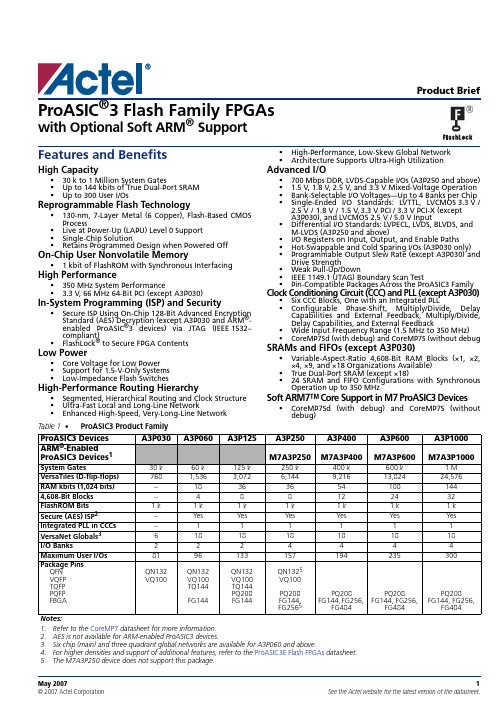
ProASIC3 Flash Family FPGAs
I/Os Per Package1
number.
2
Product Brief
元器件交易网
ProASIC3 Ordering Information
ProASIC3 Flash Family FPGAs
A3P1000 _ 1
FGBiblioteka G144I
Application (Temperature Range)
Blank = Commercial (0°C to +70°C) I = Industrial (–40°C to +85°C)
RAM kbits (1,024 bits)
4,608-Bit Blocks
FlashROM Bits Secure (AES) ISP2
Integrated PLL in CCCs VersaNet Globals3
I/O Banks
Maximum User I/Os
Package Pins QFN VQFP TQFP PQFP FBGA
元器件交易网
ProASIC®3 Flash Family FPGAs
with Optional Soft ARM® Support
Product Brief ®
Features and Benefits
High Capacity
• 30 k to 1 Million System Gates • Up to 144 kbits of True Dual-Port SRAM • Up to 300 User I/Os
电气常识)
电气常识)1、基尔霍夫定理的内容是什么?〔仕兰微电子〕基尔霍夫电流定律是一个电荷守恒定律,即在一个电路中流入一个节点的电荷与流出同一个节点的电荷相等.基尔霍夫电压定律是一个能量守恒定律,即在一个回路中回路电压之和为零.2、平板电容公式(C=εS/4πkd)。
〔未知〕3、最基本的如三极管曲线特性。
〔未知〕4、描画反应电路的概念,罗列他们的运用。
〔仕兰微电子〕5、负反应种类〔电压并联反应,电流串联反应,电压串联反应和电流并联反应〕;负反应的优点〔降低缩小器的增益灵敏度,改动输入电阻和输入电阻,改善缩小器的线性和非线性失真,有效地扩展缩小器的通频带,自动调理作用〕〔未知〕6、缩小电路的频率补偿的目的是什么,有哪些方法?〔仕兰微电子〕7、频率照应,如:怎样才算是动摇的,如何改动频响曲线的几个方法。
〔未知〕8、给出一个查分运放,如何相位补偿,并画补偿后的波特图。
〔凹凸〕9、基本缩小电路种类〔电压缩小器,电流缩小器,互导缩小器和互阻缩小器〕,优缺点,特别是普遍采用差分结构的缘由。
〔未知〕10、给出一差分电路,通知其输入电压Y+和Y-,求共模重量和差模重量。
〔未知〕11、画差放的两个输入管。
〔凹凸〕12、画出由运放构成加法、减法、微分、积分运算的电路原理图。
并画出一个晶体管级的运放电路。
〔仕兰微电子〕13、用运算缩小器组成一个10倍的缩小器。
〔未知〕14、给出一个复杂电路,让你剖析输入电压的特性〔就是个积分电路〕,并求输入端某点的rise/fall时间。
(Infineon口试试题)15、电阻R和电容C串联,输入电压为R和C之间的电压,输入电压区分为C上电压和R 上电压,要求制这两种电路输入电压的频谱,判别这两种电路何为高通滤波器,何为低通滤波器。
当RC<< period - setup ? hold16、时钟周期为T,触发器D1的树立时间最大为T1max,最小为T1min。
组合逻辑电路最大延迟为T2max,最小为T2min。
电子信息工程、自动化、通信工程、电气类等专业面试将会遇到试题大全

模拟电路1 、基尔霍夫定理的内容是什么?(仕兰微电子)基尔霍夫电流定律是一个电荷守恒定律 ,即在一个电路中流入一个节点的电荷与流出同一个节点的电荷相等 .基尔霍夫电压定律是一个能量守恒定律 ,即在一个回路中回路电压之和为零 .2、平板电容公式(C=εS/4πkd)。
(未知)3、最基本的如三极管曲线特性。
(未知)4、描述反馈电路的概念,列举他们的应用。
(仕兰微电子)5、负反馈种类(电压并联反馈,电流串联反馈,电压串联反馈和电流并联反馈);负反馈的优点 (降低放大器的增益灵敏度,改变输入电阻和输出电阻,改善放大器的线性和非线性失真,有效地扩展放大器的通频带,自动调节作用)(未知)6、放大电路的频率补偿的目的是什么,有哪些方法?(仕兰微电子)7、频率响应,如:怎么才算是稳定的,如何改变频响曲线的几个方法。
(未知)8、给出一个查分运放,如何相位补偿,并画补偿后的波特图。
(凹凸)9、基本放大电路种类(电压放大器,电流放大器,互导放大器和互阻放大器),优缺点,特别是广泛采用差分结构的原因。
(未知)10、给出一差分电路,告诉其输出电压 Y+和 Y-,求共模分量和差模分量。
(未知)11、画差放的两个输入管。
(凹凸)12、画出由运放构成加法、减法、微分、积分运算的电路原理图。
并画出一个晶体管级的运放电路。
(仕兰微电子)13、用运算放大器组成一个 10 倍的放大器。
(未知)14、给出一个简单电路,让你分析输出电压的特性(就是个积分电路),并求输出端某点的 rise/fall 时间。
(Infineon 笔试试题)15、电阻 R 和电容 C 串联,输入电压为 R 和 C 之间的电压,输出电压分别为 C 上电压和 R 上电压,要求制这两种电路输入电压的频谱,判断这两种电路何为高通滤波器,何为低通滤波器。
当 RC<< period - setup ? hold16、时钟周期为 T,触发器 D1 的建立时间最大为 T1max,最小为 T1min。
FPGA面试题
1、同步电路和异步电路的区别是什么?(仕兰微电子)2、什么是同步逻辑和异步逻辑?(汉王笔试)同步逻辑是时钟之间有固定的因果关系.异步逻辑是各时钟之间没有固定的因果关系.3、什么是"线与"逻辑,要实现它,在硬件特性上有什么具体要求?(汉王笔试)线与逻辑是两个输出信号相连可以实现与的功能.在硬件上,要用oc门来实现,由于不用oc门可能使灌电流过大,而烧坏逻辑门. 同时在输出端口应加一个上拉电阻.4、什么是Setup 和Holdup时间?(汉王笔试)5、setup和holdup时间,区别.(南山之桥)6、解释setup time和hold time的定义和在时钟信号延迟时的变化.(未知)7、解释setup和hold time violation,画图说明,并说明解决办法.(威盛VIA上海笔试试题)Setup/hold time 是测试芯片对输入信号和时钟信号之间的时间要求.建立时间是指触发器的时钟信号上升沿到来以前,数据稳定不变的时间.输入信号应提前时钟上升沿(如上升沿有效)T时间到达芯片,这个T就是建立时间-Setup time.如不满足setup time,这个数据就不能被这一时钟打入触发器,只有在下一个时钟上升沿,数据才能被打入触发器. 保持时间是指触发器的时钟信号上升沿到来以后,数据稳定不变的时间.如果hold time 不够,数据同样不能被打入触发器. 建立时间(Setup Time)和保持时间(Hold time).建立时间是指在时钟边沿前,数据信号需要保持不变的时间.保持时间是指时钟跳变边沿后数据信号需要保持不变的时间.如果不满足建立和保持时间的话,那么DFF将不能正确地采样到数据,将会出现metastability的情况.如果数据信号在时钟沿触发前后持续的时间均超过建立和保持时间,那么超过量就分别被称为建立时间裕量和保持时间裕量.8、说说对数字逻辑中的竞争和冒险的理解,并举例说明竞争和冒险怎样消除.(仕兰微电子)9、什么是竞争与冒险现象?怎样判断?如何消除?(汉王笔试)在组合逻辑中,由于门的输入信号通路中经过了不同的延时,导致到达该门的时间不一致叫竞争.产生毛刺叫冒险.如果布尔式中有相反的信号则可能产生竞争和冒险现象.解决方法:一是添加布尔式的消去项,二是在芯片外部加电容.10、你知道那些常用逻辑电平?TTL与COMS电平可以直接互连吗?(汉王笔试)常用逻辑电平:12V,5V,3.3V;TTL和CMOS不可以直接互连,由于TTL是在0.3-3.6V之间,而CMOS则是有在12V的有在5V的.CMOS输出接到TTL是可以直接互连.TTL接到CMOS需要在输出端口加一上拉电阻接到5V或者12V.11、如何解决亚稳态.(飞利浦-大唐笔试)亚稳态是指触发器无法在某个规定时间段内达到一个可确认的状态.当一个触发器进入亚稳态时,既无法预测该单元的输出电平,也无法预测何时输出才能稳定在某个正确的电平上.在这个稳定期间,触发器输出一些中间级电平,或者可能处于振荡状态,并且这种无用的输出电平可以沿信号通道上的各个触发器级联式传播下去.12、IC设计中同步复位与异步复位的区别.(南山之桥)同步复位就是指复位信号只有在时钟上升沿到来时,才能有效。
ds180_7Series_Overview
© Copyright 2010–2013 Xilinx, Inc., Xilinx, the Xilinx logo, Artix, ISE, Kintex, Spartan, Virtex, Vivado, Zynq, and other designated brands included herein are trademarks of Xilinx in the United States and other countries. PCI Express is a trademark of PCI-SIG and used under license. All other trademarks are the property of their respective owners.General DescriptionXilinx® 7series FPGAs comprise three new FPGA families that address the complete range of system requirements, ranging from low cost, small form factor, cost-sensitive, high-volume applications to ultra high-end connectivity bandwidth, logic capacity, and signal processing capability for the most demanding high-performance applications. The 7series FPGAs include:•Artix®-7 Family: Optimized for lowest cost and power with small form-factor packaging for the highest volume applications.•Kintex®-7 Family: Optimized for best price-performance with a 2X improvement compared to previous generation, enabling a new class of FPGAs.•Virtex®-7 Family: Optimized for highest system performance and capacity with a 2X improvement in system performance. Highest capability devices enabled by stacked silicon interconnect (SSI) technology.Built on a state-of-the-art, high-performance, low-power (HPL), 28nm, high-k metal gate (HKMG) process technology, 7series FPGAs enable anunparalleled increase in system performance with 2.9Tb/s of I/O bandwidth, 2 million logic cell capacity, and 5.3TMAC/s DSP , while consuming 50% less power than previous generation devices to offer a fully programmable alternative to ASSPs and ASICs.Summary of 7Series FPGA Features•Advanced high-performance FPGA logic based on real 6-input look-up table (LUT) technology configurable as distributed memory.•36Kb dual-port block RAM with built-in FIFO logic for on-chip data buffering.•High-performance SelectIO™ technology with support for DDR3 interfaces up to 1,866 Mb/s.•High-speed serial connectivity with built-in multi-gigabit transceivers from 600Mb/s to maximum rates of 6.6Gb/s up to 28.05Gb/s, offering a special low-power mode, optimized for chip-to-chip interfaces.• A user configurable analog interface (XADC), incorporating dual 12-bit 1MSPS analog-to-digital converters with on-chip thermal and supply sensors.•DSP slices with 25x 18 multiplier, 48-bit accumulator, and pre-adder for high performance filtering, including optimized symmetric coefficient filtering.•Powerful clock management tiles (CMT), combining phase-locked loop (PLL) and mixed-mode clock manager (MMCM) blocks for high precision and low jitter.•Integrated block for PCI Express® (PCIe), for up to x8 Gen3 Endpoint and Root Port designs.•Wide variety of configuration options, including support forcommodity memories, 256-bit AES encryption with HMAC/SHA-256 authentication, and built-in SEU detection and correction.•Low-cost, wire-bond, lidless flip-chip, and high signal integrity flip-chip packaging offering easy migration between family members in the same package. All packages available in Pb-free and selected packages in Pb option.•Designed for high performance and lowest power with 28nm, HKMG, HPL process, 1.0V core voltage process technology and 0.9V core voltage option for even lower power.7Series FPGAs OverviewDS180 (v1.14) July 29, 2013Advance Product SpecificationTable 1:7Series Families ComparisonMaximum CapabilityArtix-7 FamilyKintex-7 FamilyVirtex-7 FamilyLogic Cells215K478K 1,955K Block RAM (1) 13Mb 34Mb 68Mb DSP Slices7401,9203,600Peak DSP Performance (2)929GMAC/s2,845GMAC/s5,335GMAC/sTransceivers163296Peak Transceiver Speed6.6Gb/s 12.5Gb/s 28.05Gb/s Peak Serial Bandwidth (Full Duplex)211Gb/s 800Gb/s 2,784Gb/s PCIe Interface x4 Gen2x8 Gen2x8 Gen3Memory Interface 1,066Mb/s1,866Mb/s1,866Mb/s I/O Pins 5005001,200I/O Voltage 1.2V , 1.35V , 1.5V , 1.8V , 2.5V , 3.3V 1.2V , 1.35V , 1.5V , 1.8V , 2.5V, 3.3V 1.2V , 1.35V , 1.5V , 1.8V, 2.5V , 3.3V Package Options Low-Cost, Wire-Bond, LidlessFlip-ChipLow-Cost, Lidless Flip-Chip and High-Performance Flip-ChipHighest Performance Flip-ChipNotes:1.Additional memory available in the form of distributed RAM.2.Peak DSP performance numbers are based on symmetrical filter implementation.Device LogicCells Configurable Logic Blocks(CLBs)DSP48E1Slices(2)Block RAM Blocks(3)CMTs(4)PCIe(5)GTPsXADCBlocksTotal I/OBanks(6)Max UserI/O(7) Slices(1)MaxDistributedRAM (Kb)18Kb36Kb Max(Kb)XC7A35T33,2805,20040090100501,80051415250 XC7A50T52,1608,150600120150752,70051415250 XC7A75T75,52011,8008921802101053,78061816300 XC7A100T101,44015,8501,1882402701354,86061816300 XC7A200T215,36033,6502,88874073036513,14010116110500 Notes:1.Each 7series FPGA slice contains four LUTs and eight flip-flops; only some slices can use their LUTs as distributed RAM or SRLs.2.Each DSP slice contains a pre-adder, a 25x18 multiplier, an adder, and an accumulator.3.Block RAMs are fundamentally 36Kb in size; each block can also be used as two independent 18Kb blocks.4.Each CMT contains one MMCM and one PLL.5.Artix-7 FPGA Interface Blocks for PCI Express support up to x4 Gen 2.6.Does not include configuration Bank 0.7.This number does not include GTP transceivers.Table 3:Artix-7 FPGA Device-Package Combinations and Maximum I/OsPackage(1)CPG236CSG324CSG325FTG256SBG484FGG484(2)FBG484(2)FGG676(3)FBG676(3)FFG1156 Size (mm)10 x 1015 x 1515 x 1517 x 1719 x 1923 x 2323 x 2327 x 2727 x 2735 x 35 Ball Pitch (mm)0.50.80.8 1.00.8 1.0 1.0 1.0 1.0 1.0Device GTPI/OGTPI/OGTPI/OGTPI/OGTPI/OGTPI/OGTPI/OGTPI/OGTPI/OGTPI/O HR(4)HR(4)HR(4)HR(4)HR(4)HR(4)HR(4)HR(4)HR(4)HR(4)XC7A35T21000210415001704250XC7A50T21000210415001704250XC7A75T0210017042858300XC7A100T0210017042858300XC7A200T42854285840016500 Notes:1.All packages listed are Pb-free. Some packages are available in Pb option.2.Devices in FGG484 and FBG484 are footprint compatible.3.Devices in FGG676 and FBG676 are footprint compatible.4.HR = High Range I/O with support for I/O voltage from 1.2V to 3.3V.Device LogicCellsConfigurable LogicBlocks (CLBs)DSPSlices(2)Block RAM Blocks(3)CMTs(4)PCIe(5)GTXs XADCBlocksTotal I/OBanks(6)MaxUserI/O(7) Slices(1)MaxDistributedRAM (Kb)18Kb36Kb Max (Kb)XC7K70T65,60010,2508382402701354,86061816300 XC7K160T162,24025,3502,18860065032511,70081818400 XC7K325T326,08050,9504,00084089044516,02010116110500 XC7K355T356,16055,6505,0881,4401,43071525,740612416300 XC7K410T406,72063,5505,6631,5401,59079528,62010116110500 XC7K420T416,96065,1505,9381,6801,67083530,060813218400 XC7K480T477,76074,6506,7881,9201,91095534,380813218400 Notes:1.Each 7series FPGA slice contains four LUTs and eight flip-flops; only some slices can use their LUTs as distributed RAM or SRLs.2.Each DSP slice contains a pre-adder, a 25x18 multiplier, an adder, and an accumulator.3.Block RAMs are fundamentally 36Kb in size; each block can also be used as two independent 18 Kb blocks.4.Each CMT contains one MMCM and one PLL.5.Kintex-7 FPGA Interface Blocks for PCI Express support up to x8 Gen 2.6.Does not include configuration Bank 0.7.This number does not include GTX transceivers.Table 5:Kintex-7 FPGA Device-Package Combinations and Maximum I/OsPackage(1)FBG484FBG676(2)FFG676(2)FBG900(3)FFG900(3)FFG901FFG1156 Size (mm)23 x 2327 x 2727 x 2731 x 3131 x 3131 x 3135 x 35 Ball Pitch(mm) 1.0 1.0 1.0 1.0 1.0 1.0 1.0Device GTXI/OGTXI/OGTXI/OGTXI/OGTXI/OGTXI/OGTXI/OHR(4)HP(5)HR(4)HP(5)HR(4)HP(5)HR(4)HP(5)HR(4)HP(5)HR(4)HP(5)HR(4)HP(5)XC7K70T41851008200100XC7K160T418510082501508250150XC7K325T825015082501501635015016350150XC7K355T243000XC7K410T825015082501501635015016350150XC7K420T283800324000 XC7K480T283800324000 Notes:1.All packages listed are Pb-free. Some packages are available in Pb option.2.Devices in FBG676 and FFG676 are footprint compatible.3.Devices in FBG900 and FFG900 are footprint compatible.4.HR = High Range I/O with support for I/O voltage from 1.2V to 3.3V.5.HP = High Performance I/O with support for I/O voltage from 1.2V to 1.8V.Table 6:Virtex-7 FPGA Feature SummaryDevice(1)LogicCellsConfigurable LogicBlocks (CLBs)DSPSlices(3)Block RAM Blocks(4)CMTs(5)PCIe(6)GTX GTH GTZXADCBlocksTotal I/OBanks(7)MaxUserI/O(8)SLRs(9) Slices(2)MaxDistributedRAM (Kb)18Kb36Kb Max(Kb)XC7V585T582,72091,0506,9381,260 1,590795 28,6201833600117850N/A XC7V2000T1,954,560305,40021,5502,160 2,5841,29246,51224436001241,2004XC7VX330T326,40051,0004,3881,1201,50075027,0001420280114700N/A XC7VX415T412,16064,4006,5252,1601,76088031,6801220480112600N/A XC7VX485T485,76075,9008,1752,8002,0601,03037,0801445600114700N/A XC7VX550T554,24086,6008,7252,8802,3601,18042,4802020800116600N/A XC7VX690T693,120108,30010,8883,6002,9401,47052,92020308001201,000N/A XC7VX980T979,200153,00013,8383,6003,0001,50054,0001830720118900N/A XC7VX1140T1,139,200178,00017,7003,3603,7601,88067,68024409601221,1004XC7VH580T580,48090,7008,8501,6801,88094033,84012204881126002XC7VH870T876,160136,90013,2752,5202,8201,41050,760183072161136503 Notes:1.EasyPath™-7 FPGAs are also available to provide a fast, simple, and risk-free solution for cost reducing Virtex-7 T and Virtex-7 XT FPGA designs2.Each 7series FPGA slice contains four LUTs and eight flip-flops; only some slices can use their LUTs as distributed RAM or SRLs.3.Each DSP slice contains a pre-adder, a 25x18 multiplier, an adder, and an accumulator.4.Block RAMs are fundamentally 36Kb in size; each block can also be used as two independent 18 Kb blocks.5.Each CMT contains one MMCM and one PLL.6.Virtex-7 T FPGA Interface Blocks for PCI Express support up to x8 Gen 2. Virtex-7 XT and Virtex-7 HT Interface Blocks for PCI Express support up to x8 Gen 3, with theexception of the XC7VX485T device, which supports x8 Gen 2.7.Does not include configuration Bank 0.8.This number does not include GTX, GTH, or GTZ transceivers.9.Super logic regions (SLRs) are the constituent parts of FPGAs that use SSI technology. Virtex-7 HT devices use SSI technology to connect SLRs with 28.05 Gb/stransceivers.Table 7:Virtex-7 FPGA Device-Package Combinations and Maximum I/Os Package(1)FFG1157FFG1761(2)FHG1761(2)FLG1925 Size (mm)35 x 3542.5 x 42.545 x 4545 x 45 Ball Pitch 1.0 1.0 1.0 1.0Device GTX GTHI/OGTX GTHI/OGTX GTHI/OGTXI/OHR(3)HP(4)HR(3)HP(4)HR(3)HP(4)HR(3) HP(4)XC7V585T2000600360100750XC7V2000T36008501601,200XC7VX330T020060002850650XC7VX415T0200600XC7VX485T20006002800700XC7VX550TXC7VX690T02006000360850XC7VX980TXC7VX1140TNotes:1.All packages listed are Pb-free. Some packages are available in Pb option.2.Devices in FFG1761 and FHG1761 are footprint compatible.3.HR = High Range I/O with support for I/O voltage from 1.2V to 3.3V.4.HP = High Performance I/O with support for I/O voltage from 1.2V to 1.8V.Table 8:Virtex-7 FPGA Device-Package Combinations and Maximum I/Os - ContinuedPackage(1)FFG1158FFG1926(2)FLG1926(2)FFG1927FFG1928(3)FLG1928(3)FFG1930(4)FLG1930(4) Size (mm)35 x 3545 x 4545 x 4545 x 4545 x 4545 x 4545 x 4545 x 45 Ball Pitch 1.0 1.0 1.0 1.0 1.0 1.0 1.0 1.0Device GTX GTH I/OGTX GTHI/OGTX GTHI/OGTX GTHI/OGTX GTHI/OGTX GTHI/OGTX GTHI/OGTX GTHI/OHP(5)HP(5)HP(5)HP(5)HP(5)HP(5)HP(5)HP(5)XC7V585TXC7V2000TXC7VX330TXC7VX415T0483********XC7VX485T480350560600240700XC7VX550T0483********XC7VX690T0483500647200806000241,000XC7VX980T064720072480024900XC7VX1140T0647200964800241,100 Notes:1.All packages listed are Pb-free. Some packages are available in Pb option.2.Devices in FFG1926 and FLG1926 are footprint compatible.3.Devices in FFG1928 and FLG1928 are footprint compatible.4.Devices in FFG1930 and FLG1930 are footprint compatible.5.HP = High Performance I/O with support for I/O voltage from 1.2V to 1.8V.Table 9:Virtex-7 FPGA Device-Package Combinations and Maximum I/Os - ContinuedPackage(1)HCG1155HCG1931HCG1932Size (mm)35 x 3545 x 4545 x 45Ball Pitch 1.0 1.0 1.0Device GTH GTZI/OGTH GTZI/OGTH GTZI/O HP(2)HP(2)HP(2)XC7VH580T248400488600488300 XC7VH870T4886507216300 Notes:1.All packages listed are Pb-free. Some packages are available in Pb option.2.HP = High Performance I/O with support for I/O voltage from 1.2V to 1.8V.Stacked Silicon Interconnect (SSI) TechnologyThere are many challenges associated with creating high capacity FPGAs that Xilinx addresses with the SSI technology. SSI technology enables multiple super logic regions (SLRs) to be combined on a passive interposer layer, using proven manufacturing and assembly techniques from industry leaders, to create a single FPGA with more than ten thousand inter-SLR connections, providing ultra-high bandwidth connectivity with low latency and low power consumption. There are two types of SLRs used in Virtex-7 FPGAs: a logic intensive SLR used in the Virtex-7 T devices and a DSP/blockRAM/transceiver-rich SLR used in the Virtex-7 XT and HT devices. SSI technology enables the production of higher capability FPGAs than traditional manufacturing methods, enabling the highest capacity and highest performance FPGAs ever created to reach production more quickly and with less risk than would otherwise be possible. Thousands of super long line (SLL) routing resources and ultra-high performance clock lines that cross between the SLRs ensure that designs span seamlessly across these high-density programmable logic devices.CLBs, Slices, and LUTsSome key features of the CLB architecture include:•Real 6-input look-up tables (LUTs)•Memory capability within the LUT•Register and shift register functionalityThe LUTs in 7 series FPGAs can be configured as either one 6-input LUT (64-bit ROMs) with one output, or as two 5-input LUTs (32-bit ROMs) with separate outputs but common addresses or logic inputs. Each LUT output can optionally be registered in a flip-flop. Four such LUTs and their eight flip-flops as well as multiplexers and arithmetic carry logic form a slice, and two slices form a configurable logic block (CLB). Four of the eight flip-flops per slice (one per LUT) can optionally be configured as latches.Between 25–50% of all slices can also use their LUTs as distributed 64-bit RAM or as 32-bit shift registers (SRL32) or as two SRL16s. Modern synthesis tools take advantage of these highly efficient logic, arithmetic, and memory features.Clock ManagementSome of the key highlights of the clock management architecture include:•High-speed buffers and routing for low-skew clock distribution•Frequency synthesis and phase shifting•Low-jitter clock generation and jitter filteringEach 7series FPGA has up to 24 clock management tiles (CMTs), each consisting of one mixed-mode clock manager (MMCM) and one phase-locked loop (PLL).Mixed-Mode Clock Manager and Phase-Locked LoopThe MMCM and PLL share many characteristics. Both can serve as a frequency synthesizer for a wide range of frequencies and as a jitter filter for incoming clocks. At the center of both components is a voltage-controlled oscillator (VCO), which speeds up and slows down depending on the input voltage it receives from the phase frequency detector (PFD).There are three sets of programmable frequency dividers: D, M, and O. The pre-divider D (programmable by configuration and afterwards via DRP) reduces the input frequency and feeds one input of the traditional PLL phase/frequency comparator. The feedback divider M (programmable by configuration and afterwards via DRP) acts as a multiplier because it divides the VCO output frequency before feeding the other input of the phase comparator. D and M must be chosen appropriately to keep the VCO within its specified frequency range. The VCO has eight equally-spaced output phases (0°, 45°, 90°, 135°, 180°, 225°, 270°, and 315°). Each can be selected to drive one of the output dividers (six for the PLL, O0 to O5, and seven for the MMCM, O0 to O6), each programmable by configuration to divide by any integer from 1 to 128. The MMCM and PLL have three input-jitter filter options: low bandwidth, high bandwidth, or optimized mode. Low-bandwidth mode has the best jitter attenuation but not the smallest phase offset. High-bandwidth mode has the best phase offset, but not the best jitter attenuation. Optimized mode allows the tools to find the best setting.MMCM Additional Programmable FeaturesThe MMCM can have a fractional counter in either the feedback path (acting as a multiplier) or in one output path. Fractional counters allow non-integer increments of 1/8 and can thus increase frequency synthesis capabilities by a factor of 8.The MMCM can also provide fixed or dynamic phase shift in small increments that depend on the VCO frequency. At 1600MHz, the phase-shift timing increment is 11.2ps.Clock DistributionEach 7series FPGA provides six different types of clock lines (BUFG, BUFR, BUFIO, BUFH, BUFMR, and the high-performance clock) to address the different clocking requirements of high fanout, short propagation delay, and extremely low skew.Global Clock LinesIn each 7series FPGA, 32 global clock lines have the highest fanout and can reach every flip-flop clock, clock enable, and set/reset, as well as many logic inputs. There are 12 global clock lines within any clock region driven by the horizontal clock buffers (BUFH). Each BUFH can be independently enabled/disabled, allowing for clocks to be turned off within a region, thereby offering fine-grain control over which clock regions consume power. Global clock lines can be driven by global clock buffers, which can also perform glitchless clock multiplexing and clock enable functions. Global clocks are often driven from the CMT, which can completely eliminate the basic clock distribution delay.Regional ClocksRegional clocks can drive all clock destinations in their region. A region is defined as any area that is 50 I/O and 50 CLB high and half the chip wide. 7series FPGAs have between six and twenty-four regions. There are four regional clock tracks in every region. Each regional clock buffer can be driven from either of four clock-capable input pins, and its frequency can optionally be divided by any integer from 1 to 8.I/O ClocksI/O clocks are especially fast and serve only I/O logic and serializer/deserializer (SerDes) circuits, as described in theI/O Logic section. The 7series devices have a direct connection from the MMCM to the I/O for low-jitter, high-performance interfaces.Block RAMSome of the key features of the block RAM include:•Dual-port 36Kb block RAM with port widths of up to 72•Programmable FIFO logic•Built-in optional error correction circuitryEvery 7series FPGA has between 50 and 1,880 dual-port block RAMs, each storing 36Kb. Each block RAM has two completely independent ports that share nothing but the stored data.Synchronous OperationEach memory access, read or write, is controlled by the clock. All inputs, data, address, clock enables, and write enables are registered. Nothing happens without a clock. The input address is always clocked, retaining data until the next operation. An optional output data pipeline register allows higher clock rates at the cost of an extra cycle of latency.During a write operation, the data output can reflect either the previously stored data, the newly written data, or can remain unchanged.Programmable Data WidthEach port can be configured as 32K×1, 16K×2, 8K×4, 4K×9 (or8), 2K×18 (or16), 1K×36 (or32), or 512×72 (or64). The two ports can have different aspect ratios without any constraints.Each block RAM can be divided into two completely independent 18Kb block RAMs that can each be configured to any aspect ratio from 16K×1 to 512×36. Everything described previously for the full 36Kb block RAM also applies to each of the smaller 18Kb block RAMs.Only in simple dual-port (SDP) mode can data widths of greater than 18bits (18Kb RAM) or 36bits (36Kb RAM) be accessed. In this mode, one port is dedicated to read operation, the other to write operation. In SDP mode, one side (read or write) can be variable, while the other is fixed to 32/36 or 64/72.Both sides of the dual-port 36Kb RAM can be of variable width.Two adjacent 36Kb block RAMs can be configured as one cascaded 64K×1 dual-port RAM without any additional logic. Error Detection and CorrectionEach 64-bit-wide block RAM can generate, store, and utilize eight additional Hamming code bits and perform single-bit error correction and double-bit error detection (ECC) during the read process. The ECC logic can also be used when writing to or reading from external 64- to 72-bit-wide memories.FIFO ControllerThe built-in FIFO controller for single-clock (synchronous) or dual-clock (asynchronous or multirate) operation increments the internal addresses and provides four handshaking flags: full, empty, almost full, and almost empty. The almost full and almost empty flags are freely programmable. Similar to the block RAM, the FIFO width and depth are programmable, but the write and read ports always have identical width.First word fall-through mode presents the first-written word on the data output even before the first read operation. After the first word has been read, there is no difference between this mode and the standard mode.Digital Signal Processing — DSP SliceSome highlights of the DSP functionality include:•25×18 two's complement multiplier/accumulator high-resolution (48bit) signal processor•Power saving pre-adder to optimize symmetrical filter applications•Advanced features: optional pipelining, optional ALU, and dedicated buses for cascadingDSP applications use many binary multipliers and accumulators, best implemented in dedicated DSP slices. All 7series FPGAs have many dedicated, full custom, low-power DSP slices, combining high speed with small size while retaining system design flexibility.Each DSP slice fundamentally consists of a dedicated 25×18 bit two's complement multiplier and a 48-bit accumulator, both capable of operating up to 741MHz. The multiplier can be dynamically bypassed, and two 48-bit inputs can feed a single-instruction-multiple-data (SIMD) arithmetic unit (dual 24-bit add/subtract/accumulate or quad 12-bitadd/subtract/accumulate), or a logic unit that can generate any one of ten different logic functions of the two operands. The DSP includes an additional pre-adder, typically used in symmetrical filters. This pre-adder improves performance in densely packed designs and reduces the DSP slice count by up to 50%. The DSP also includes a 48-bit-wide Pattern Detector that can be used for convergent or symmetric rounding. The pattern detector is also capable of implementing96-bit-wide logic functions when used in conjunction with the logic unit.The DSP slice provides extensive pipelining and extension capabilities that enhance the speed and efficiency of many applications beyond digital signal processing, such as wide dynamic bus shifters, memory address generators, wide bus multiplexers, and memory-mapped I/O register files. The accumulator can also be used as a synchronous up/down counter.Input/OutputSome highlights of the input/output functionality include:•High-performance SelectIO technology with support for 1,866Mb/s DDR3•High-frequency decoupling capacitors within the package for enhanced signal integrity•Digitally Controlled Impedance that can be 3-stated for lowest power, high-speed I/O operationThe number of I/O pins varies depending on device and package size. Each I/O is configurable and can comply with a large number of I/O standards. With the exception of the supply pins and a few dedicated configuration pins, all other package pins have the same I/O capabilities, constrained only by certain banking rules. The I/O in 7series FPGAs are classed as High Range (HR) or High Performance (HP). The HR I/Os offer the widest range of voltage support, from 1.2V to 3.3V. The HP I/Os are optimized for highest performance operation, from 1.2V to 1.8V.HR and HP I/O pins in 7 series FPGAs are organized in banks, with 50 pins per bank. Each bank has one common V CCO output supply, which also powers certain input buffers. Some single-ended input buffers require an internally generated or an externally applied reference voltage (V REF). There are two V REF pins per bank (except configuration bank 0). A single bank can have only one V REF voltage value.Xilinx 7series FPGAs use a variety of package types to suit the needs of the user, including small form factor wire-bond packages for lowest cost; conventional, high performance flip-chip packages; and lidless flip-chip packages that balance smaller form factor with high performance. In the flip-chip packages, the silicon device is attached to the package substrate using a high-performance flip-chip process. Controlled ESR discrete decoupling capacitors are mounted on the package substrate to optimize signal integrity under simultaneous switching of outputs (SSO) conditions.I/O Electrical CharacteristicsSingle-ended outputs use a conventional CMOS push/pull output structure driving High towards V CCO or Low towards ground, and can be put into a high-Z state. The system designer can specify the slew rate and the output strength. The input is always active but is usually ignored while the output is active. Each pin can optionally have a weak pull-up or a weak pull-down resistor.Most signal pin pairs can be configured as differential input pairs or output pairs. Differential input pin pairs can optionally be terminated with a 100Ω internal resistor. All 7series devices support differential standards beyond LVDS: HT, RSDS, BLVDS, differential SSTL, and differential HSTL.Each of the I/Os supports memory I/O standards, such as single-ended and differential HSTL as well as single-ended SSTL and differential SSTL. The SSTL I/O standard can support data rates of up to 1,866Mb/s for DDR3 interfacing applications. 3-State Digitally Controlled Impedance and Low Power I/O FeaturesThe 3-state Digitally Controlled Impedance (T_DCI) can control the output drive impedance (series termination) or can provide parallel termination of an input signal to V CCO or split (Thevenin) termination to V CCO/2. This allows users to eliminate off-chip termination for signals using T_DCI. In addition to board space savings, the termination automatically turns off when in output mode or when 3-stated, saving considerable power compared to off-chip termination. The I/Os also have low power modes for IBUF and IDELAY to provide further power savings, especially when used to implement memory interfaces.I/O LogicInput and Output DelayAll inputs and outputs can be configured as either combinatorial or registered. Double data rate (DDR) is supported by all inputs and outputs. Any input and some outputs can be individually delayed by up to 32 increments of 78ps or 52ps each. Such delays are implemented as IDELAY and ODELAY. The number of delay steps can be set by configuration and can also be incremented or decremented while in use.。
TPS5430中文资料_数据手册_参数
1 Features
•1 4.5-V to 28-V Wide Input Voltage Range • Integrated 85-mΩ and 40-mΩ MOSFETs for 3-A,
Continuous Output Current • Low 2-μA Shutdown, 45-μA Quiescent Current • Internal 5-mS Soft-Start • Fixed 400-kHz Switching Frequency • Frequency Spread Spectrum to Reduce EMI • Advanced Eco-mode™ Pulse Skip • Peak Current Mode Control • Internal Loop Compensation • Overcurrent Protection for Both MOSFETs with
7.3 Feature Description................................................... 9 7.4 Device Functional Modes........................................ 12 8 Application and Implementation ........................ 13 8.1 Application Information............................................ 13 8.2 Typical Application ................................................. 13 9 Power Supply Recommendations...................... 20 10 Layout................................................................... 21 10.1 Layout Guidelines ................................................. 21 10.2 Layout Example .................................................... 21 11 Device and Documentation Support ................. 22 11.1 Community Resources.......................................... 22 11.2 Trademarks ........................................................... 22 11.3 Electrostatic Discharge Caution ............................ 22 11.4 Glossary ................................................................ 22 12 Mechanical, Packaging, and Orderable Information ........................................................... 22
R5F212A7SNFA中文资料
A/D Converter
10-bit resolution × 12 channels, includes sample and hold function
D/A Converter Flash Memory
8-bit resolution × 2 circuits • Programming and erasure voltage: VCC = 2.7 to 5.5 V
Timer RC
shot generation mode
16 bits × 1 (with 4 capture/compare registers) Timer mode (input capture function, output compare function), PWM mode
Timer RD
Memory
ROM, RAM
Power Supply Voltage detection
Voltage
ciperation mode: Single-chip mode (address space: 1 Mbyte) Refer to Table 1.5 Product List for R8C/2A Group. • Power-on reset • Voltage detection 2
Table 1.1 Specifications for R8C/2A Group (1)
Item CPU
Function
Specification
Central processing R8C/Tiny series core
unit
• Number of fundamental instructions: 89
circuits