电极设计
毕业设计_电火花成型中的电极设计

南京信息职业技术学院毕业设计论文作者学号系部机电学院专业数控技术题目模具制造中的电火花成型的应用指导教师李新华评阅教师完成时间:年月日毕业设计中文摘要毕业设计外文摘要目录引言模具工业的迅速发展,推动了模具制造技术的进步。
电火花加工作为模具制造技术的一个重要分支,被赋予越来越高的加工要求。
同时在数控加工技术发展新形势的影响下,促使电火花加工技术朝着更深层次、更高水平的数控化方向快速发展。
虽然模具高速加工技术的迅猛发展使电加工面临着严峻的挑战,目前放电加工技术部分工序已被高速加工中心代替,但电火花加工仍旧有广阔的前景。
如在模具的复杂、精密小型腔、窄缝、沟槽、拐角、冒孔、深度切削等加工领域仍被广泛应用。
电火花机床的基本知识电火花原理通过间隙自动控制系统控制工具电极向工件进给,当两电极间的间隙达到一定距离时,两电极上施加的脉冲电压将工作液击穿,产生火花放电。
在放电的微细通道中瞬时集中大量的热能,温度可高达万摄氏度以上,压力也有急剧变化,从而使这一点工作表面局部微量的金属材料立刻熔化、气化,并爆炸式地飞溅到工作液中,迅速冷凝,形成固体的金属微粒,被工作液带走。
这时在工件表面上便留下一个微小的凹坑痕迹,放电短暂停歇,两电极间工作液恢复绝缘状态。
紧接着,下一个脉冲电压又在两电极相对接近的另一点处击穿,产生火花放电,重复上述过程。
这样,虽然每个脉冲放电蚀除的金属量极少,但因每秒有成千上万次脉冲放电作用,就能蚀除较多的金属,具有一定的生产率。
在保持工具电极与工件之间恒定放电间隙的条件下,一边蚀除工件金属,一边使工具电极不断地向工件进给,最后便加工出与工具电极形状相对应的形状来。
因此,只要改变工具电极的形状和工具电极与工件之间的相对运动方式,就能加工出各种复杂的型面。
电火花的优点与缺点优点()适合于难切削材料的加工。
电火花加工中,材料的加工性能主要取决于材料的热学性能,而几乎与力学性能(硬度、韧性、抗拉强度)无关,突破传统切削加工对刀具的限制。
大型工业硅电炉的电极系统设计
大型工业硅电炉的电极系统设计李桂红中钢集团吉林机电设备有限公司吉林132021摘要:本文通过对云南永昌铅锌股份有限公司25.5MV·A半密闭、全液压、炉体旋转式的大型工业硅电炉的电极系统的设计及对电极把持、电极升降、电极压放形式的论述,系统地计算了电极升降、压放和把持时所需的液压力、蝶形弹簧力。
详细的论述了电极把持、升降、压放装置的结构形式和工作原理。
重点介绍了根据冶炼工艺要求,如何把液压系统的液压力与把持电极和传输电流时分别所需的压力、电极压放所需的压放力、蝶形弹簧的弹力有机地协调起来,根据电极的重量科学地设定液压系统的压力,可在冶炼操作时实现有序的电极升降和压放。
使电极的升降、压放程序与炉料的选择、电炉的操作结合起来,坚持做到精心选料、优化设备、科学操作,就可实现国家发改委提倡的环保、节能、优质、高产、低耗、高效工业硅生产,进而实现工业硅产品的深加工。
关键词:方式设计形式设计计算1.前言我国工业硅电炉生产,已有很多年的历史,经过多年来在原料上精选,设备上完善,技术上提高,工业硅生产不断发展。
大容量工业硅电炉属国家发改委提倡的环保、节能、优质、高产、低耗、高效型电炉。
同时,也是各生产企业企盼已久的生产工业硅产品进而实现该产品深加工的理想炉型。
大型工业硅电炉生产所需要的原料、设备、操作是三个主要环节,在电炉设计、制作、生产操作过程中,只要始终坚持并做到精心选料、优化设计、科学操作,就可实现我国工业硅生产电炉向大型化发展。
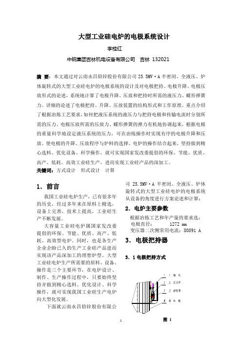
下面就云南永昌铅锌股份有限公司25.5MV·A半密闭、全液压、炉体旋转式的大型工业硅电炉的电极系统从设备的角度进行方案论述和计算:2.电炉主要参数根据冶炼工艺和年产量的要求选:电极直径: 1272 mm变压器二次侧常用电流:80891 A 3.电极把持器3.1电极把持方式图书LTU本方案电极把持方式采用压力环方式。
此种方式为铜瓦压紧电极是通过波纹管伸缩箱充压力油来实现的。
有源拉普拉斯电极的设计
分 器 , 其 对 交 流 信 号 没 有 作 用 ,只 对 直 流 和 极 低 频
信 号 积 分 ,抵 消 其 影 响 ,从 而 解 决 了 放 大 后 的 失 调
转 换 器 的 输 入 ) 饱 和 。而 实 际 应 用 中 ,对 于 一 个 多
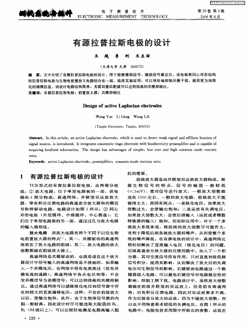
器 ,带 有 积 分 反 馈 电 路 的 高 通 差 分 放 大 器 和 共 模 信
号 取 样 驱 动 电 路 , 电 路 设 计 如 图 1所 示 ; ② 同 心 环 形 电极 ( 层 圆环 、 中部 圆环 、 中心 圆盘 ) 它 外 ,
要 :文 中介绍 了有源拉普拉斯 电极 的设 计 ,用 于检测 微弱信 号 ,辅 助信号 源定 位。该 电极将 同心环形 结构
的拉普拉斯 电极与生物电前置放大 电路结合在 一起 ,临 床实 验证 明 ,可 以很 好地抑 制共模 干扰 ,提供更 为局部 化 的细微信 息 。该设计 电路结构简单 ,无需刻意匹配就可 以达到很 高 的共模抑制 比。
关键词 :有 源拉普拉斯 电极 ;前置放 大器 ;共模抑制 比
De i n o c ie La l c a ee t o s sg f a tv p a i n lc r de
W a g Yu Li n W a l n e g Ga g n Li i
( a nUnv ri ,Ta j 3 0 7 ) Ti  ̄i ies y ini 0 0 2 t n,
据 生 物 信 号 的 特 点 ,信 号 的 幅 值 一 般 较 低 ( 1 < mV),需 对 信 号 进 行 放 大 , 一 般 放 大 倍 数 都 选在 10 0 0左 右 。一 般 的 放 大 电 路 , 前 级 放 大 不 能 做 得 太 大 ,原 因有 两 点 :一 是 极 化 电 压 ,如 果 放 大 倍 数 过 大 ,会 使 输 出 饱 和 ; 二 是 运 放 有 失 调 电 压 , 如 果 放 大 倍 数 太 大 ,会 使 后 级 输 入 ( 放 或 者 模 数 运
电极设置步骤

电极设置步骤第一步:打开软件如下图所示,并找到电极设置命令。
第二步:打开这个界面,如下,并调入零件模型-创建新的文件夹-点击确定键即可:第三步:点击确定键以后将进入电极设计模块的界面,这里面包含下图所示的内容:第四步:进入了电极设计界面以后,我们就按照向导条的顺序向下继续操作下去。
1.首先就是提取电极,提取电极就是提取你所要进行放电加工的地方,看上图中几个凹槽的地方都是要么是死角要么是无法加工到位的沟槽,而电极加工的目的就是解决这么尖角和沟槽用数控加工中心加工不到位的地方。
2.确定好以后我们点击特征树里面的灯,将模具隐藏起来,只留下提取出来的面:3.然后将鼠标放在特征树里的电极上,点右键“激活”当前电极4.激活以后可以按照向导条的指示继续下面的操作。
4.点击毛坯图标可以出现下面对话框5.如果上面的相关参数你需要修改,直接进行参数设置就可以了,原始数值都是针对当前电极软件推荐的数值。
仅供参考。
6.参数设置好以后,我们点击确定键就可以继续下步操作。
7.毛坯设置好以后,我们就可以做电极坐标系的设置,点击电极坐标系的图标,在每个电极中都会有3个点可供我们做电极坐标系:8.电极坐标系做好以后,我们就可以寻找电极延伸面的轮廓,而有人要问为什么不做电极柄,这个电极柄的作用是起着夹持电极和通电的,所以这个电极柄可以不用特别去研究。
下面我们直接进行电极延伸面的轮廓,点击自动轮廓图标:。
会出现下面对话框:9.点击确定以后,就可以做好电极了:10. 电极设计好以后,点击激活装配图标:,然后就可以出电极图纸了,并进行电极仿真:11.在特征树里点击电极并点右键:12.电极图纸如下:13.可以使用电极设计模板。
电极规范2010.03.20

、筋条电极(筋条小口≤1.50mm)。
1-2条电极墨筋条电极电极数量火花间隙1 件一般为-0.2 mm1-3放电体积(v) 电极数量≤20x20x20 2件≥v≥20x20x20 2件(1粗1精)≥v≥40x40x40 2件(1粗1精)3件(1粗2精 /其一:两侧面。
拖表时,两侧面的竖向方向拖过后,在任选一侧面拖横向方向,即可校正电极因此电极设计时,特别是较大的电极,可选择适合的基准来设计,达到减小电极体积、省料的目的,如图:3、所有电极的座台高度(Z 2)需≥20mm(因为背面钻螺钉孔深度为15 —19mm )否则容易钻穿,通常为20mm。
1-6电极座台顶面相邻两边(不需四边)要凸出7mm(平面,不含R角,即X / X1表用(托表指针端为R1;常用靠数基准球为R5)和靠数用。
拖表的基准面的长度应大于被校正的面的长度的三分之一。
电极的造型:电极的外形不可太小,至少要大于12×12×20mm,以方便电火花人员进行靠数基准角一般做成C3,电极尺寸较大时则可做大。
尺寸要求较高时,需分粗精打,同一个电极的精打电极要倒斜角,粗打电极要倒定模上的电极的R角需全部重倒(成锐角的面重倒时变化大,需注意适当重倒或将该电极分粗精打,、在其他方式不好加工时,可考虑设计成靠模,靠模仍可按普通电极设计,只是线切割加工时分别加工出电极头和电极座台,然后将电极头装入电极座台,即成靠模。
出火花图时必须以电极头的顶点靠数。
如图:电极设计由于在造型上不能扣火花间隙的电极,可交由编程人员扣火花间隙。
火花间隙为整体放(整个电极含电极头、座台等整体扣火花间隙),需在电极造型上刻字,如“产品面与分型面的电极,能分开尽量分开。
如工件上斜顶槽的产品面与靠破面相交接的地方,电极不能延伸,需止于分型面,否则易导致产品飞边、溢料。
在设计动模侧的电极前,需先确定是否要将小镶块装在大镶块里一起打,若要,则先取单独动模大镶块上配合处的电极,再取单独动模大镶块上产品处及其他电极,之后再取小镶块、斜顶上需单独打的电极,最后将小镶块、斜顶、顶针等装入动模后一起取;若不装在一起打,则优先取动小镶块和大镶块面分别有筋。
电极设计方法及原则94页PPT

6、最大的骄傲于最大的自卑都表示心灵的最软弱无力。——斯宾诺莎 7、自知之明是最难得的知识。——西班牙 8、勇气通往天堂,怯懦通往地狱。——塞内加 9、有时候读书是一种巧妙地避开思考的方法。——赫尔普斯 10、阅读一切好书如同和过去最杰出的人谈话。——笛卡儿
电极设计方法及原则
21、没有人陪你走一辈子,所以你要 适应孤 独,没 有人会 帮你一 辈子, 所以你 要奋斗 一生。 22、当眼泪流尽的时候,留下的应该 是坚强 。 23、要改变命运,首先改变自己。
24、勇气很有理斯顿. 丘吉尔 。 25、梯子的梯阶从来不是用来搁脚的 ,它只 是让人 们的脚 放上一 段时间 ,以便 让别一 只脚能 够再往 上登。
Thank you
电容式触控面板电极布局之设计与分析.
Computer Aided Design of Electrode Pattern in Capacitive Touch Panel s ¥: ¿T: ·E ¤ ~ ¤(Visual Basic for Application)µyUoiXMpuCuiNqeOWqAuhwqNiHteXq×CuiHYupq×Aqu×AiHuhta×q×CbqXAiHBDpqiHoqu×CApueX×X10.2TqeOCVBA Tq10.2AOPzjiHABniBqeBqCqu×OvTqeOIImAqGOvTqu×DAHhMOq×hqu×CPepper (1983)´Xq×hqu×ALoq×OhBsqCTalmage (1987)´XFtq×ALoqAh OPqHCDunthorn (1991)µoFbYhOPqCoXgmiHDhHq×hqCMAbpPoq×OOAHbFXpPRxAYusqeOyCPDA¡AGibson MTq×OVBA (Visual Basic for Application)µyoMpuAuNqoAKiHBtapXPoq×CouOwqAbWhwqnqXoCAAgXRCboputFAbiHhwqq×~HmXhqHXoCGiHhwqXATiHMwCpqGAiHwqCpqoCbuX12.2Tq×PMq×iCAA(Active Area)°PeA~iHwqnAA(Active Area)°aCquiHPmqCNqqVOVOYuqAPmqpCpuftoCGsX1.3%¡AqXu×TqeOCqu×1.77%¡C 10.21. ¥XFXpPRvCqu×qeODnAqGvTqCFMpuAuNqoAKiHBtapXPoq×CRGNAiHpuftt×q×C2. °puOwqAbWwqqXoCAAgXRCpiHtwqq×AYuFcq×CBpuXq×BiC3. ±qCPqXGiHDnWYmqAiHWWemqOArea)°aCquiHPmqCNqqVOVOYuqAPmqpCpuftCGsXqXu×10.2TqeOCqu×1.77%¡C AutoCADqUpuyA AsqeOyVBA (Visual Basic for Application)µyo12.2Tq×PMNmqAA(Active 1.3%¡ACOMPUTER AIDED DESIGN OF ELECTRODE PATTERN INCAPACITIVE TOUCH PANELStudent: Chung-Wen LaiAdvisor: Shih-Ming YangABSTRACTThis thesis aims at developing an efficient method for designing the electrode pattern in capacitive touch panel. The linearity of the electrical field on the capacitive touch panel is very important to the quality of the touch panel, and the distribution of silver electrodes on the panel is the key to improve the electric field.A parametric design tool is established under the Visual Basic for Application (VBA) program language. The dimensions of the silver electrode are parameterized in this parametric design tool. The electrode pattern can be established by defining these parameters. This tool not only can shorten the time of designing the electrode pattern, but also can adjust the geometry of silver electrodes easily. A 12.2 inch electrode pattern is designed by using this parametric design tool to prove the feasibility of this tool. Seven kinds of element geometry test can be used to adjust the layout of the silverelectrodes for good linearity. Finally, a 10.2 inch electrode pattern is fabricated and validated.iCONTENTSPage ABSTRACT (i)CONTENTS (ii)LIST OF TABLES (iii)LIST OF FIGURES (iv)Chapter 1 Introduction1.1 Motivation (1)1.2 Types of Touch Panels (1)1.3 Literature Review (4)1.4 Outline (7)Chapter 2 Parametric Design Tool of Electrode Pattern in Touch Panel2.1 CAD on Electrode Board (12)2.2 The Idea of Establishing Model (13)2.3 Drawing and Analyzing the 12.2 Inch Electrode Pattern (16)2.4 Conclusion (17)Chapter 3 Design and Analysis of Electrode Pattern on Capacitive Touch Panel3.1 Introduction (28)3.2 The Test of Element Geometry (28)3.3 Design an Electrode Pattern on 10.2 Inch Capacitive Touch Panel (35)3.4 Fabricating the 10.2 Inch Capacitive Touch Panel (39)3.5 Conclusion (40)Chapter 4 Summary and Conclusions References…..…………………………………………………………………….…62 ii LIST OF TABLESTable Page1.1 Comparison of Touch Panel (4)2.1 Element Geometry in Electrode Pattern Design (15)3.1 Single Element Test on Changing the Length (29)3.2 Integral Element Test on Changing the Length (29)3.3 Single Element Test on Changing the Width (31)3.4 Integral Element Test on Changing the Width (31)3.5 Single Element Test on Changin g the Position (32)3.6 Integral Element Test on Changing the Position (32)3.7 Single Element Test on Changing the Geometry (33)3.8 Integral Element Test on Changing the Geometry (33)3.9 Single Element Test on Changing the Distance between Two Elements (34)3.10 Integral Element Test on Changing the Distance between Two Elements (34)3.11 Single Element Test on Cutting the Element in Horizontal Direction (34)3.12 Integral Element Tes t on Cutting the Element in Horizontal Direction (34)3.13 Single Element Test on Cutting the Element in Vertical Direction (35)3.14 Integral Element Test on Cutting the Element in Vertical Direction (35)iiiLIST OF FIGURESFigure Page1.1 Th e structure and the work process of optic type touch panel (8)1.2 The structure and the work process of acoustic wave type touch panel (9)1.3 The structure and the work process of capacitive type touch panel (10)1.4 The structure a nd the work process of resistive type touch panel (11)2.1 The user interface of VBA (19)2.2 The work process of designing the electrode pattern (20)2.3 The first parametric dialogue box of electrode pattern design (21)2.4 The second parametric dialogue box of electrode pattern design (22)2.5 The third parametric dialogue box of electrode pattern design (23)2.6 The fourth parametric dialogue box of electrode pattern design (24)2.7 The analysis result of designed pattern in vertical direction (25)2.8 The analysis result of designed pattern in horizontal direction (25)2.9 The user interface of ANSYS (26)2.10 The geometry of U.S. patent (27)2.11 The analysis result of U.S. patent in horizontal direction (27)3.1 The method of measuring the voltage (42)3.2 (a) The length change (b) The width change (43)3.3 The first equipotential line and the interval between two equipotential lines (44)3.4 (a) The position change (b) The geometry change (c) The interval change (45)3.5 (a) The horizontal cut (b) The vertical cut (46)3.6 The g eometry of middle element (47)3.7 The initial electrode pattern (48)3.8 The horizontal electric field of the initial electrode pattern (49)iv3.9 The position of the ideal equipotential lines (50)3.10 The middle element and edge element adjustment (51)3.11 The element of the third part adjustment (52)3.12 The vertical electric field of the initial electrode pattern (53)3.13 The final electrode pattern (54)3.14 The horizontal electric field of the final electrode pattern (55)3.15 The process of fabricating the touch panel (56)3.16 The eGalax company controller (57)3.17 The 10.2 inch capacitive touch panel (58)3.18 The linearity test on the 10.2 inch capacitive touch panel (59)vChapter 1Introduction1.1 MotivationTouch panels are integrated directly onto the screen and they make products lighter and smaller with added portability and convenience. In addition, they can eliminate unskilled users’ fear of using computers. Application products of touch panel including PDA, mobile telephone, GPS navigate panel, e-book, ATM. The aim of this study is integrating with the design and the analysis on electrode pattern of capacitive touch panel. The linearity of the electric field is very important and the layout of silver electrodes influences the linearity of the touch panel directly. Many researches on improving the linearity of the touch panel are presented. However, spending the time on designing the electrode pattern in any size is a serious defect. Visual Basic for Application (VBA) program language is utilized to develop a parametric design tool. The dimensions of the silver electrode are parameterized and the electrode pattern can be established by defining these parameters. This parametric design tool and the function of changing the coordinates on an object in AutoCAD can be used to revise the electrode pattern when the analysis result is unsatisfied.The parametric dialogue box utilized in this tool can simplify the process of constructing the model. In addition, the test of element geometry can be used to adjust the geometry of the silver electrodes for good linearity. The user not only can have aninitial concept on designing the electrode pattern by these testing results but also can shorten the time of designing the electrode pattern.1.2 Types of Touch PanelsThe touch panel application can be divided from personal digital devices to popular facilities devices; mechanics and size of products used in different fields are not the same. 1And the technological principle of touch panel can be divided into following several kinds:(1) Optic type:The component device of optic type touch panel includes glass substrate; infrared light emitting diode (LED) and infrared ray receiver, an array of LED/receiver pairs are mounted on two opposite sides to create a grid of invisible infrared light. It is to utilize the principle of receiving the light source. Touch panel is covered with light source and receiver and made up matrix there. When a user touches the display resulting in obstructing one or more of the light beam, receivers from each axis will detect the absence of light and transmit signals that identify the X and Y coordinates to the computer as shown in Fig. 1.1. The advantage of the optic type touch panel is good dependability and transmittance. The optic type touch panel is applied on ATM, medical system, etc.(2) Acoustic wave type:Acoustic wave type touch panel is made of transmitting transducers, receiving transducers, reflectors, and a controller. Transmitting transducers are located along the horizontal and the vertical edges of a glass plate and receiving transducers are located at the opposite edges of the glass plate. The acoustic wave technology uses inaudible sound waves traveling over the surface of a glass panel. First, the electrical signal is conveyed from controller to the transmitting transducer, and the electrical signal will be transferred to acoustic wave, furthermore, it passes through the surface of glass plate to an array of reflectors directly. Reflectors on the opposite side gather and direct the waves to the receiving transducer, which reconverts them into an electrical signal. Finally, the signal will be transmitted back to the controller that saves the normal condition information. When a user touches the screen, the finger will absorb some acoustic waves, the wave form will be changed at this moment, and this reduced energy will be detected, then the X or Y coordinate location will be calculated as shown in Fig.1.2. The advantage of the acoustic 2wave type touch panel is good protection and higher dots per inch. It is applied for kiosk, and automatic ticket system.(3) Capacitive type:A glass substrate is plated a conductive layer and then an electrode pattern is made on it, finally, covering with a protective layer on the surface. The principle of capacitive touch panel is giving voltages on four corners of the screen to make a stable electric field, when a user touches the screen, transparent electrode and static electricity with the human body that produces the capacitance change, then according to the inducing current to measure its coordinates as shown in Fig. 1.3. Because it is only printed electrodes and transmitted the signals on one glass, so the transmittance of capacitive touch panel is over 90% better than resistive type touch panel. It is good at preventing the dust and the damage, furthermore it has fast response. It is applied for ATM, outdoor guide system, etc.(4) Resistive type:It consists of a pair of ITO conductive layers, spacer dots, and an electrode layer. ITO glass is used to be a substrate covered with an ITO film above, and spreading spacer dots between the ITO glass and ITO film to prevent contact, afterwards printing the silver electrodes along the edge to provide a voltage. When using, a voltage is alternately applied to the horizontal and the vertical axes. When the upper layer is pressed and contacting with the upper conductive layer, that voltage is sensed and sent to a controller that contains an analog-to-digital converter. The voltage is converted to a digital X or Y to indicate the touch location as shown in Fig. 1.4. It is because that the resistive type touch panel is induced by pressure, so there is no limit about touching medium. Therefore, it is applied in the environment without the limitation of touching medium, for instance, supervisory control apparatus, PDA, and industry control, etc. The comparison 3of touch panels is shown in Table 1.1.Table 1.1 Comparison of Touch Panel. (From Ho, 2003)ResolutionOptical clarityTouch life Infrared Acoustic 1024×1024 About 1200/sq. in80~85% Millions 100% Many millionsAbout 1200/sq. in 100000/sq. in92% Many millions 75~85% Many millionsVery1.3 Literature ReviewThe touch panel appeared in 1974, but it came to maturity until that Siemens Corporation proposed Elographics soft glass sensors in 1977. The technologies of touch panel and products have been applied in our daily life more than ten years. Touchpanels were limited by the cost in early stages, so putting on the public machine platforms, and POS/POI (Point of Sales/Point of Information) is the main application. With the change of communication technology and the trend of lighter, smaller, shorter of information products in recent years, in addition, the computer operation system is transferred to GUI (Graphic User Interface) that prompts the computer system more user-friendly. And it is because that the mouse and the keyboard are too big to carry, so the touch panel becomes the standard equipment of portable products.Many researches showed the method to enhance the accuracy of determining the touching point. The way of improving the capacitive touch panel can be divided into reforming the controller and mending the electrode pattern to enhance the linearity of the electrical field. Many means have been done to enhance the precision of converting the 4current signal into the touching coordinate via improving the method of controlling the capacitive touch panel. Pepper (1981) proposed a general method for accurately determining the location or position of a source or sink of electric current on the surface of a resistance element or impedance layer. Touch panel embodiment determines the position of the user’s finger from currents caused by ambient electrical noise. Krein and Meadows (1988) presented a quasistatic electric field applied to a semiconducting coating on the capacitive touch panel surface. A touch draws current from the surface; this current can be used to compute position. If the computation is performed properly, the computed position is independent of touch current and panel coating resistivity. Jhang (2003) proposed a method of controlling the capacitive touch panel. After inputting the stable alternating voltage, the current obtained is amplified. The current difference before and after touching is converted to get the touching coordinate. The above study improves the controller of capacitive touch panel. However, the adjustment of determining the touch point by the controller is limited as the linearity of the electrical field is bad. So the key of enhancing the precision of determining the touching point is improving the electrode pattern. The different electrode patterns invented are described in the following articles.Pepper (1983) invented the edge terminations to provide linearization of the electric field. The edge terminations are constituted by a series of parallel ranks or rows of connective segments overlaid, inlaid or printed at each edge of the polygonal surface with the innermost row or rank being short straight segments and the length of each segment of the next innermost row, respectively, being longer. The central segment in each row or rank is electrically interconnected with the central segments in the other rows. Jheng (2002) proposed an improved touch panel by changing the layout of theresistance conductive lines. Several resistance conductive lines are set on the surface of the touch 5panel. The resistive lines in the one of the regions are smaller than others. It is because that to let the every region has same voltages. By this way, the touch panel can decide the touch point accurately. The concept of establishing the electrode pattern by a series of parallel ranks or rows of silver lines in above patents is utilized on a parametric design tool developed in this thesis. So a user can decide the number of parallel ranks or rows of silver lines. However, when the aspect ratio of the monitor is changed, the fixed electrode pattern in this patent can not support the touch panel for good linearity. Therefore, the parametric design tool can be used to construct any size electrode pattern. Bloom et al. (1986) presented an improved touch panel and a method that increasing the percentage of useful area of a touch-sensitive panel includes electrode elements in electrical communication with an electrically conductive layer of known spatial impedance characteristics. The touch panel structure incorporates improved electrode structure and electrode to impedance layer interfacing elements which impact a more linear mapping function within an expanded touch-sensitive region of the resistive layer. The touch panel can be utilized in a general touch-mapping system without resort to extensive mapping coordinate correction apparatus of earlier systems. Although the percentage of useful area of a touch panel is increased, the region set the silver lines is too large to a touch panel in the present day. And the linearity of the electrical field produced by the layout of an electrode pattern in this patent can’t achieve the demand at present. The area of setting the silver lines can be controlled in this design tool and the linearity can be adjusted by this tool as analysis result is unsatisfied.Gibson and Talmage (1987) showed a resistor electrode type touch sensor having enhanced area of linear response by reducing the bow in perimeters of the sensor and the method of accomplishing the same. Dunthorn (1991) reported a resistor type of gradient sheet for a touch sensor having reduced ripple and bow of equipotential lines along edges 6and in the corners of the sensor. T-shaped electrodes of a selected effective length and spacing are attached to the resistive surface, the length and spacing selected to substantially eliminate the bow of the equipotential fields. The above two works, although the electrode pattern is invented to improve the linearity, the time of adjusting the size of electrode pattern in any size is too long. The concept of revising the pattern can be obtained by the result of element geometry test in this thesis. So the time of establishing the electrode pattern can be reduced.Frey et al. (2003) showed the interest of using finite element simulations in association with partial discharge measurements to determine and localize the maximum field values. Myatt and Marston (1994) presented a coupled electromagnetic and nonlinear structural analysis of a 4.5 tesla superconducting MHD dipole magnet. From the above technical literature, they take a long time to construct the model in ANSYS. In this thesis, the platform of establishing the model is developed. The model is parameterized to shorten the time of constructing and the analysis process is simplified.1.4 OutlineThe motivation of this thesis is described in chapter 1. Then it is introduced with four kind principles of touch panel and there are many people improve the touch panel and create numerous new technologies are introduced in literature review. In chapter 2, it is explained that how to operate the VBA to develop the parametric design tool and the idea of wiring is also illustrated. Afterwards, the parametric design tool is utilized to draw a 12.2 inch electrode pattern. Then the feasibility of the design process is proved by importing the electrode pattern to ANSYS. In chapter 3, seven element geometry tests are used to let the users realize how to adjust the layout of electrode pattern and the 10.2 inch electrode pattern on capacitive touch panel is drawn and fabricated. Finally, there is a conclusion about whole thesis in chapter 4.7Edge of ActiveDisplay Area Opto-Matrix Frame Inside Bezel Grid of Infrared Light Inside and Outside Edges of Infrared TransparentFigure 1.1 The structure and the work process of optic type touch panel. (From ELO TouchSystem)8Transducers Transducers TransducersReflections on each axis divertThe ultrasonic burst across the touchscreenFigure 1.2 The structure and the work process of acoustic wave type touch panel. (From ELO TouchSystem)9Process andComponentsClearTek 3000 OvercoatFinishedSensor Product Electrode PatternConductive CoatingGlassConductive CoatingMinute amount of voltage applied toall corners of touch screenUniform electric fieldTouch draws current from eachcorner of electric field controllerMeasures the ratio of currents todetermine touch locationFigure 1.3 The structure and the work process of capacitive type touch panel. (From 3M TouchSystem)10ITO conductive layerSpacer dotITO conductive coatingGlass bottom circuit layer Top circuit layer Hard coat on surface A flexible hard-coated polyester filmis overlaid on a rigid glass layerFigure 1.4 The structure and the work process of resistive type touch panel.(From ELO TouchSystem)11Chapter 2A Parametric Design Tool of Electrode Pattern in Touch Panel2.1 CAD on Electrode BoardFrom the principle of the capacitive touch panel, the linearity of electric field is very important. The key of influencing the linearity of electric field is the layout of the electrode pattern. So analyzing the electrical field of the electrode layer is very important. In this thesis, Visual Basic for Application (VBA) program language is utilized that interface is shown in Fig. 2.1 in which AutoCAD is to develop a parametric design tool for designing electrode pattern fast, furthermore collocating with ANSYS is computer aided analysis software to analyze and simulate.As to VBA, it is an object-oriented programming environment and it supplies the function of developing that similar to Visual Basic language. In general, the main discrepancy between VB and VBA is executing in the same procedure space with AutoCAD, providing an intelligent AutoCAD and a speedy program design environment. In addition, VBA also can integrate other application programs, which have VBA ability. It means that AutoCAD can be an automation controller in other application programs, for instance, Microsoft Word or Excel. VBA will transmit the messages through the AutoCAD ActiveX Automation interface to the AutoCAD, and AutoCAD also permits VBA environment and AutoCAD can implement at the sametime. Therefore, the way of combination for AutoCAD, ActiveX Automation, and VBA supplies powerful interface, not only can control internal objects of AutoCAD but can transmit or get information between other application programs. There are four advantages for using VBA: 1. VBA is learned and used easily under the Visual Basic language environment, 2. VBA and AutoCAD are operated in the same procedure, it means that the programs can be executed very fast, 3. dialogue boxes are established fast and effectively, that let developer 12prototypes application programs and gets the response of design fast, and 4. projects can be independent or set in the drawings, this flexible selection supplies developers on sending to other application programs. To the general finite element analysis software, for instance, I-DEAS, PATRAN, NASTRAN, MARC, etc., the way to analyze is importing the entity's model directly and utilizes solution module to analyze, if the users are unsatisfied with the analysis result, and wants to revise the part of model, they must revise entity's model again, imports to the software and analyzes again, makes the process of analysis seems long.VBA is utilized to develop a set of parameter type design tool. The size of the silver lines is parameterized by this tool. So long as a user follows the dialogue box to design the pattern and then can execute analysis fast, shortening the time of construction the model in the analysis. The process of designing the electrode pattern is shown in Fig. 2.2. The electrode pattern is established by using a parametric tool under the AutoCAD design software. Then this electrode pattern model is exported in IGES (Initial Graphics Exchange Specification) file type and it is imported to the computer aided analysis software to read and establish the model. There are two methods for building analysis model in computer aided analysis software; here GUI (Graphic User Interface) is utilized to obtain various electrical field effects of electrode pattern and electrical field uniformity. The above-mentioned using parametric language designs electrode patterns include the width and the length of silver electrode, and geometry of electrode board. After supplying the power to a transparent electrode of touch panel, the electrical field uniformity of whole touch panel should be cared. If the linearity is not good, it will decrease the accuracy that controller determines the position. So analyzing electrical field linearity of whole electrode board is a key to estimate the quality of touch panels.2.2 The Idea of Establishing ModelIt is beginning to introduce the concept of this parametric design tool. 1/4 of the 13 electrode pattern is set up and then the whole panel is established by the way of reflection are initial thought. First, the frame size of the touch panel has to be confirmed. The method is deciding the length and the width of the frame of the touch panel.Afterward, defining the length and the width of AA district (active area) is the next step. The parametric dialogue box is illustrated in Fig. 2.3.The length and the width of the frame and AA district are parameterized. It lets users revise the size of the touch panel easily. And then a region set the silver electrodes is detected between the frame and AA district. This region can be subdivided into several small areas on this design idea. To clarity the description, the silver electrodes printed on ITO substrate are called the picture element and as long as it can be drawn under the AutoCAD software that can be joined and used. There are four kinds of elements supported to choose as shown in Table. 2.1. The picture element chosen will be put in each small area and the elements will be reproduced in 1/4 of the panel by the way of the reflection and then the elements in 1/4 of the panel are set to the whole panel in the same way.The reason of reflecting the elements in this way is simplifying the design complexity. Thus the layout of the electrode pattern is getting symmetrical. This way can improve the linearity of the touch panel after analyzing the electric field and achieve the final purpose of developing this parametric design tool. The four corners of the whole electrode pattern are applied voltages. So they must be designed separately. Because of considering the symmetrical relation, the edge elements on the corner are all the same. The geometry of the edge element is not important to affect the linearity of the electric field. So only the length and width of the edge element is defined. According to Gibson and Talmage (1987), non-uniformity electric field near the perimeter of the AA district is produced by the voltage drop. It means that the equipotential line near the edge would be a curve line. 14So the middle element is also designed separately to improve this defect as shown in Fig.2.4.。
电极设计规范
门
会ቤተ መጻሕፍቲ ባይዱ
签
可
另
附
页
部门
意见
签字
日期
编程
EDM
质量
起草部门意见:
主管部门意见:
审
核
分管领导意见:
批准
总经理:
青岛麦瑞模具供应链有限公司
程 序 文 件
编号
ZZ-53
页次
1/1
版本
V1
生效期
2012-11-10
主题:
电极设计规范
1.目的:规范电极设计基本要求杜绝电蚀加工异常
2.范围:青岛麦瑞模具供应链有限公司
模具类型
加工位置
粗公火花位
精公火花位
备注
汽车、家电模具
分型面、插碰穿面
胶位面
粗公可根据电极大小调整火花位
筋位厚度小于
精密模具
分型面、插碰穿面
胶位面
筋位厚度小于
5.4.电极清角设计:
汽车类模具在拆电极时,没有特别要求的情况下,转角为尖角的位置无需分拆,在电极图上注明手工清尖角,由钳工做清角处理,以防止电极数量多,增加放电时间;
青岛麦瑞模具供应链有限公司
程序文件会签表
编号
版本
A/0
生效期
2011-11-16
文件名称
电极设计规范
起草人
陈丕新
起草部门
加工部
说明:本文件属□新增;□修订。本文件编号为ZZ-53,第1次修改。
本文制定修改的目的是:规范电极设计基本要求杜绝电蚀加工异常。
文件涉及部门:编程、质量、EDM
2012年11月10日
5.5.组合电极设计:
拆电极时考虑放电质量的同时也应该充分考虑放电的效率,电极数量较多并且高度相仿,属性相仿的电极,拆电极时应考虑用铝板工装一次放电的办法,以防止电极数量多,增加放电时间;
MT电极设计规范
如图 1-4
图 1-3
图 1-5
6. 电极对刀台的底面,需刻上电极粗精公的编号。侧面模具刻图档号,字的大小不能 小于 1.2mm.如图 1-5
二、 工程图的要求:
1. 标题栏应包括 A. 模具编号 B 工件编号 C 铜公编号 C 客户 D 工件类型 :E 粗、精公的火花位及
数量 F 制图人 G 审核 H 制图时间 I 流程 J 公司名称。如图 2-1 的内容。
3. 为提高加工效率,非成形部分做成直身位。 如图 1-2
4. 冲水位高度不小于 5mm。如图 1-3
图 1-1
5. 对刀台的高度不小于 20mm。一边的总长不 小于 20mm。XY 轴校表位预设单边最少不 能低于 5mm。C 角与基准同向。尺寸为 C3。 其余三个角倒 R1。如图 1-4
图 1-2
MT 精密塑胶模具有限公司
制 模 部
电极设计规范
一、 图档管理、取名规则
1. 图档必须从主管处取图。
A. 每一台电脑都需建立一个电极设计的总目录,名 字为 MT-EDM;
B. 每一套模具的电极设计目录名为模具号+EDM。 并放置于总目录 MT-EDM 下。
C. 每一套模具的电极设计目录下再建立每一类型的 电极设计目录,名字为模具号+类型+EDM,如模 具 号 为 2513 的 前 模 电 极 设 计 目 录 名 为 “2513A-EDM。
如模具号为 2513 前模第 5 号粗、精公的图档号为 2513A-05
3) 电极图层设置规定
A. 参照零件及参考坐标放置 240 层。
B. 相同电极需放在同一层,不同电极要分层放置。最好图层与编号一致。
C. 暂时不用的对象置于 200 层。
光学式溶解氧电极的电路设计
光学式溶解氧电极的电路设计
光学式溶解氧电极是一种用于测量水中溶解氧浓度的传感器,
它利用氧分子对光的吸收特性来测量溶解氧的含量。
下面我将从电
路设计的角度对光学式溶解氧电极进行详细的回答。
首先,光学式溶解氧电极的电路设计需要考虑到光源、光电探
测器、信号放大和处理电路等部分。
光源通常采用LED作为光源,LED的选择需要考虑到波长和功率的匹配,以确保光源能够有效地
激发溶解氧传感膜的荧光发射。
光电探测器则用于接收溶解氧传感
膜发射的荧光信号,常用的光电探测器包括光电二极管(photodiode)或光电转换器。
其次,信号放大和处理电路是光学式溶解氧电极电路设计中至
关重要的一部分。
荧光信号较弱,需要通过放大电路进行信号放大,以提高信噪比和测量精度。
放大电路通常包括前置放大器和滤波器,用于放大和滤除杂散信号。
此外,还需要采用模数转换器(ADC)将
模拟信号转换为数字信号,以便于微处理器或其他数字设备进行处
理和显示。
另外,光学式溶解氧电极的电路设计还需要考虑到电源管理和
温度补偿等问题。
电路需要稳定的电源供应以确保测量的准确性和稳定性。
同时,温度对溶解氧的测量也有影响,因此需要考虑温度补偿电路,以消除温度变化对测量结果的影响。
总的来说,光学式溶解氧电极的电路设计需要综合考虑光源、光电探测器、信号放大和处理电路、电源管理和温度补偿等多个方面,以确保测量的准确性和稳定性。
在设计过程中需要充分考虑传感器的特性和测量环境的要求,选择合适的元器件和电路方案,进行严谨的电路设计和测试验证。