DETAILED STUDY ON LARGE AREA 100% SOG SILICON MC SOLAR CELLS WITH EFFICIENCIES EXCEEDING 16%
中电光伏PERC电池研发和量产 赵建华

PSTR&D InnovationPSTR&D Innovation中电光伏PERC电池研发和量产进展赵建华中电电气(南京)光伏有限公司中电电气南京电力科技有限公司Confidential & ProprietaryCopyright ©2015 the CSUN Company Page 1 Confidential & Proprietary • Copyright © 2015 The CSUN CompanyPSTR&D Innovation太阳电池的发展历史25.6%日本松下201425%世界纪录晶硅太阳电池效率发展史Confidential & ProprietaryCopyright ©2015 the CSUN Company Page 22PSTR&D InnovationPERC (passivated emitter and rear cell) structurefinger"inverted" pyramids"inverted" pyram idsn +n p silicon oxide p-silicon t t2 mm oxiderear contact PERC (passivated emitter and Confidential & ProprietaryCopyright ©2015 the CSUN CompanyPERC (passivated emitter and rear) cell structure.PSTR&D InnovationOutline1.研发项目背景介绍2.研发历程3.研发进展总结Confidential & Proprietary Copyright ©2015 the CSUN Company Page 4PSTR&D Innovation1.中电光伏的PERC电池研发项目背景介绍中电光伏的PERC电池研发项目是依托于2012年的国家863科研课题:效率20%以上基于高效背场和背钝化技术的晶体硅电池产业化成套关键技术及示范生产线,目标是研究开发背面钝化PERC低成本高效电池,并建成一条35MW高效(大于20%)单晶硅太阳电池示范线.Confidential & Proprietary Copyright ©2015 the CSUN Company Page 5PSTR&D Innovation1.中电光伏的PERC电池研发项目背景介绍技术路线1基于氧化硅钝化的实验室PERC 电池技术路线2基于氧化铝钝化的量产的PERC 电池1电池进行研发期间尝试了多种技术方案1.中电光伏最早于2008年开始针对PERC 电池进行研发,期间尝试了多种技术方案;2.经反复实验评估,最终确定了一条实验室研发技术路线,并在此基础上优化配置出一条最有潜力的量产技术路线并于年年底实现量产Confidential & ProprietaryCopyright ©2015 the CSUN CompanyPage 6技术路线,并于2014年年底实现量产。
PbI2

Remnant PbI2, an unforeseen necessity in high-efficiency hybrid perovskite-based solar cells?a)Duyen H. Cao, Constantinos C. Stoumpos, Christos D. Malliakas, Michael J. Katz, Omar K. Farha, Joseph T. Hupp, and Mercouri G. KanatzidisCitation: APL Materials 2, 091101 (2014); doi: 10.1063/1.4895038View online: /10.1063/1.4895038View Table of Contents: /content/aip/journal/aplmater/2/9?ver=pdfcovPublished by the AIP PublishingArticles you may be interested inParameters influencing the deposition of methylammonium lead halide iodide in hole conductor free perovskite-based solar cellsAPL Mat. 2, 081502 (2014); 10.1063/1.4885548Air stability of TiO2/PbS colloidal nanoparticle solar cells and its impact on power efficiencyAppl. Phys. Lett. 99, 063512 (2011); 10.1063/1.3617469High efficiency mesoporous titanium oxide PbS quantum dot solar cells at low temperatureAppl. Phys. Lett. 97, 043106 (2010); 10.1063/1.3459146Near-IR activity of hybrid solar cells: Enhancement of efficiency by dissociating excitons generated in PbS nanoparticlesAppl. Phys. Lett. 96, 073505 (2010); 10.1063/1.3292183Effects of molecular interface modification in hybrid organic-inorganic photovoltaic cellsJ. Appl. Phys. 101, 114503 (2007); 10.1063/1.2737977APL MATERIALS2,091101(2014)Remnant PbI2,an unforeseen necessity in high-efficiency hybrid perovskite-based solar cells?aDuyen H.Cao,1Constantinos C.Stoumpos,1Christos D.Malliakas,1Michael J.Katz,1Omar K.Farha,1,2Joseph T.Hupp,1,band Mercouri G.Kanatzidis1,b1Department of Chemistry,and Argonne-Northwestern Solar Energy Research(ANSER)Center,Northwestern University,2145Sheridan Road,Evanston,Illinois60208,USA2Department of Chemistry,Faculty of Science,King Abdulaziz University,Jeddah,Saudi Arabia(Received2May2014;accepted26August2014;published online18September2014)Perovskite-containing solar cells were fabricated in a two-step procedure in whichPbI2is deposited via spin-coating and subsequently converted to the CH3NH3PbI3perovskite by dipping in a solution of CH3NH3I.By varying the dipping time from5s to2h,we observe that the device performance shows an unexpectedly remark-able trend.At dipping times below15min the current density and voltage of thedevice are enhanced from10.1mA/cm2and933mV(5s)to15.1mA/cm2and1036mV(15min).However,upon further conversion,the current density decreases to9.7mA/cm2and846mV after2h.Based on X-ray diffraction data,we determinedthat remnant PbI2is always present in these devices.Work function and dark currentmeasurements showed that the remnant PbI2has a beneficial effect and acts as ablocking layer between the TiO2semiconductor and the perovskite itself reducingthe probability of back electron transfer(charge recombination).Furthermore,wefind that increased dipping time leads to an increase in the size of perovskite crys-tals at the perovskite-hole-transporting material interface.Overall,approximately15min dipping time(∼2%unconverted PbI2)is necessary for achieving optimaldevice efficiency.©2014Author(s).All article content,except where otherwisenoted,is licensed under a Creative Commons Attribution3.0Unported License.[/10.1063/1.4895038]With the global growth in energy demand and with compelling climate-related environmental concerns,alternatives to the use of non-renewable and noxious fossil fuels are needed.1One such alternative energy resource,and arguably the only legitimate long-term solution,is solar energy. Photovoltaic devices which are capable of converting the photonflux to electricity are one such device.2Over the last2years,halide hybrid perovskite-based solar cells with high efficiency have engendered enormous interest in the photovoltaic community.3,4Among the perovskite choices, methylammonium lead iodide(MAPbI3)has become the archetypal light absorber.Recently,how-ever,Sn-based perovskites have been successfully implemented in functional solar cells.5,6MAPbI3 is an attractive light absorber due to its extraordinary absorption coefficient of1.5×104cm−1 at550nm;7it would take roughly1μm of material to absorb99%of theflux at550nm.Further-more,with a band gap of1.55eV(800nm),assuming an external quantum efficiency of90%,a maximum current density of ca.23mA/cm2is attainable with MAPbI3.Recent reports have commented on the variability in device performance as a function of perovskite layer fabrication.8In our laboratory,we too have observed that seemingly identicalfilmsa Invited for the Perovskite Solar Cells special topic.b Authors to whom correspondence should be addressed.Electronic addresses:j-hupp@ and m-kanatzidis@2,091101-12166-532X/2014/2(9)/091101/7©Author(s)2014FIG.1.X-ray diffraction patterns of CH3NH3PbI3films with increasing dipping time(%composition of PbI2was determined by Rietveld analysis(see Sec.S3of the supplementary material for the Rietveld analysis details).have markedly different device performance.For example,when ourfilms of PbI2are exposed to MAI for several seconds(ca.60s),then a light brown coloredfilm is obtained rather than the black color commonly observed for bulk MAPbI3(see Sec.S2of the supplementary material for the optical band gap of bulk MAPbI3).23This brown color suggests only partial conversion to MAPbI3and yields solar cells exhibiting a J sc of13.4mA/cm2and a V oc of960mV;these values are significantly below the21.3mA/cm2and1000mV obtained by others.4Under the hypothesis that fully converted films will achieve optimal light harvesting efficiency,we increased the conversion time from seconds to2h.Unexpectedly,the2-h dipping device did not show an improved photovoltaic response(J sc =9.7mA/cm2,V oc=846mV)even though conversion to MAPbI3appeared to be complete.With the only obvious difference between these two devices being the dipping time,we hypothesized that the degree of conversion of PbI2to the MAPbI3perovskite is an important parameter in obtaining optimal device performance.We thus set out to understand the correlation between the method of fabrication of the MAPbI3layer,the precise chemical compositions,and both the physical and photo-physical properties of thefilm.We report here that remnant PbI2is crucial in forming a barrier layer to electron interception/recombination leading to optimized J sc and V oc in these hybrid perovskite-based solar cells.We constructed perovskite-containing devices using a two-step deposition method according to a reported procedure with some modifications.4(see Sec.S1of the supplementary material for the experimental details).23MAPbI3-containing photo-anodes were made by varying the dipping time of the PbI2-coated photo-anode in MAI solution.In order to minimize the effects from unforeseen variables,care was taken to ensure that allfilms were prepared in an identical manner.The composi-tions offinal MAPbI3-containingfilms were monitored by X-ray diffraction(XRD).Independently of the dipping times,only theβ-phase of the MAPbI3is formed(Figure1).9However,in addition to theβ-phase,allfilms also showed the presence of unconverted PbI2(Figure1,marked with*) which can be most easily observed via the(001)and(003)reflections at2θ=12.56◦and38.54◦respectively.As the dipping time is increased,the intensities of PbI2reflections decrease with a concomitant increase in the MAPbI3intensities.In addition to the decrease in peak intensities of PbI2,the peak width increases as the dipping time increases indicating that the size of the PbI2 crystallites is decreasing,as expected,and the converse is observed for the MAPbI3reflections.This observation suggests that the conversion process begins from the surface of the PbI2crystallites and proceeds toward the center where the crystallite domain size of the MAPbI3phase increases and that of PbI2diminishes.Interestingly,the remnant PbI2phase can be seen in the data of other reports, but has not been identified as a primary source of variability in cell performance.8,10 Considering that the perovskite is the primary light absorber within the device,we wantedto further investigate how the optical absorption of thefilm changes with increasing dipping timeFIG.2.Absorption spectra of CH3NH3PbI3films as a function of unconverted PbI2phase fraction.FIG.3.(a)J-V curves and(b)EQE of CH3NH3PbI3-based devices as a function of unconverted PbI2phase fraction.(Figure2).11,12The pure PbI2film shows a band gap of2.40eV,consistent with the yellow color of PbI2.As the PbI2film is gradually converted to the perovskite,the band gap is progressively shifted toward1.60eV.The deviation of MAPbI3’s band gap(1.60eV)from that of the bulk MAPbI3 material(1.55eV)could be explained by quantum confinement effects related with the sizes of TiO2and MAPbI3crystallites and their interfacial interaction.13,14Interestingly,we also noticed the presence of a second absorption in the light absorber layer,in which the gap gradually red shifts from1.90eV to1.50eV as the PbI2concentration is decreased from9.5%to0.3%(Figure2—blue arrow).Having established the chemical compositions and optical properties of the light absorberfilms, we proceeded to examine the photo-physical responses of the corresponding functional devices in order to determine how the remnant PbI2affects device performance.The pure PbI2based device remarkably achieved a0.4%efficiency with a J sc of2.1mA/cm2and a V oc of564mV (Figure3(a)).Upon progressive conversion of the PbI2layer to MAPbI3,we observe two different regions(Figure4,Table I).In thefirst region,the expected behavior is observed;as more PbI2is converted to MAPbI3,the trend is toward higher photovoltaic efficiency,due both to J sc and V oc, until1.7%PbI2is reached.The increase in J sc is attributable,at least in part,to increasing absorption of light by the perovskite.We speculate that progressive elimination of PbI2,present as a layer between TiO2and the perovskite,also leads to higher net yields for electron injection into TiO2and therefore,higher J values.For a sufficiently thick PbI2spacer layer,electron injection would occur instepwise fashion,i.e.,perovskite→PbI2→TiO2.Finally,the photovoltage increase is attributable toFIG.4.Summary of J-V data vs.PbI2concentration of CH3NH3PbI3-based devices(Region1:0to15min dipping time, Region2:15min to2h dipping time).TABLE I.Photovoltaic performance of CH3NH3PbI3-based devices as a function of unconverted PbI2fraction.Dipping time PbI2concentration a J sc(mA/cm2)V oc(V)Fill factor(%)Efficiency(%) 0s100% 2.10.564320.45s9.5%10.10.93352 4.960s7.2%13.40.96052 6.72min 5.3%14.00.964557.45min 3.7%14.70.995578.315min 1.7%15.1 1.036629.730min0.8%13.60.968648.51h0.4%12.40.938657.62h0.3%9.70.84668 5.5a Determined from the Rietveld analysis of X-ray diffraction data.the positive shift in TiO2’s quasi-Fermi level as the population of photo-injected electrons is higher with increased concentration of MAPbI3.The second region yields a notably different trend;surprisingly,below a concentration of2% PbI2,J sc,V oc,and ultimatelyηdecrease.Considering that the light-harvesting efficiency would increase when the remaining2%PbI2is converted to MAPbI3(albeit to only a small degree),then the remnant PbI2must have some other role.We posit that remnant PbI2serves to inhibit detrimental electron-transfer processes(Figure5).Two such processes are back electron transfer from TiO2to holes in the valence band of the perovskite(charge-recombination)or to the holes in the HOMO of the HTM(charge-interception).This retardation of electron interception/recombination observation is reminiscent of the behavior of atomic layer deposited Al2O3/ZrO2layers that have been employed in dye-sensitized solar cells.15–18It is conceivable that the conversion of PbI2to MAPbI3occurs from the solution interface toward the TiO2/PbI2interface and thus would leave sandwiched between TiO2and MAPbI3a blocking layer of PbI2that inhibits charge-interception/recombination.For this hypothesis to be correct,it is crucial that the conduction-band-edge energy(E cb)of the PbI2be higher than the E cb of the TiO2.19–21 The work function of PbI2was measured by ultraviolet photoelectron spectroscopy(UPS)and was observed to be at6.35eV vs.vacuum level,which is0.9eV lower than the valence-band-edge energy(E vb)of MAPbI3(see Sec.S7of the supplementary material23for the work function of PbI2);the E cb(4.05eV)was calculated by subtracting the work function from the band gap(2.30eV).solar cell.FIG.6.Dark current of CH3NH3PbI3-based devices as a function of unconverted PbI2phase fraction.The E cb of PbI2is0.26eV higher than the E cb of TiO2and thus PbI2satisfies the conditions of a charge-recombination/interception barrier layer.In order to probe the hypothesis that PbI2acts as a charge-interception barrier,dark current measurements,in which electronsflow from TiO2to the HOMO of the HTM,were made.Consistent with our hypothesis,Figure6illustrates that the onset of the dark current occurs at lower potentials as the PbI2concentration decreases.In the absence of other effects,the increasing dark current with increasing fraction of perovskite(and decreasing fraction of PbI2)should result in progressively lower open-circuit photovoltages.Instead,the photocurrent density and the open-circuit photovoltage bothincrease,at least until to PbI2fraction reaches1.7%.As discussed above,thinning of a PbI2-basedFIG.7.Cross-sectional SEM images of CH3NH3PbI3film with different dipping time.sandwich layer should lead to higher net injection yields,but excessive thinning would diminish the effectiveness of PbI2as a barrier layer for back electron transfer reactions.Given the surprising role of remnant PbI2in these devices,we further probed the two-step conversion process by using scanning-electron microscopy(SEM)(Figure7).Two domains of lead-containing materials(PbI2and MAPbI3)are present.Thefirst domain is sited within the mesoporous TiO2network(area1)while the second grows on top of the network(area2).Area2initially contains 200nm crystals.As the dipping time is increased,the crystals show marked changes in size and morphology.The formation of bigger perovskite crystals is likely the result of the thermodynamically driven Ostwald ripening process,i.e.,smaller perovskite crystals dissolves and re-deposits onto larger perovskite crystals.22The rate of charge-interception,as measured via dark current,is proportional to the contact area between the perovskite and the HTM.Thus,the eventual formation of large, high-aspect-ratio crystals,as shown in Figure7,may well lead to increases in contact area and thereby contributes to the dark-current in Figure6.Regardless,we found that the formation of large perovskite crystals greatly decreased our success rate in constructing high-functioning,non-shorting solar cells.In summary,residual PbI2appears to play an important role in boosting overall efficiencies for CH3NH3PbI3-containing photovoltaics.PbI2’s role appears to be that of a TiO2-supported blocking layer,thereby slowing rates of electron(TiO2)/hole(perovskite)recombination,as well as decreasing rates of electron interception by the hole-transporting material.Optimal performance for energy conversion is observed when ca.98%of the initially present PbI2has been converted to the perovskite. Conversion to this extent requires about15min.Pushing beyond98%(and beyond15min of reaction time)diminishes cell performance and diminishes the success rate in constructing non-shorting cells.The latter problem is evidently a consequence of conversion of small and more-or-less uniformly packed perovskite crystallites to larger,poorly packed crystallites of varying shape and size.Finally,the essential,but previously unrecognized,role played by remnant PbI2 provides an additional explanation for why cells prepared dissolving and then depositing pre-formed CH3NH3PbI3generally under-perform those prepared via the intermediacy of PbI2.We thank Prof.Tobin Marks for use of the solar simulator and EQE measurement system. Electron microscopy was done at the Electron Probe Instrumentation Center(EPIC)at Northwestern University.Ultraviolet Photoemission Spectroscopy was done at the Keck Interdisciplinary SurfaceScience facility(Keck-II)at Northwestern University.This research was supported as part of theANSER Center,an Energy Frontier Research Center funded by the U.S Department of Energy, Office of Science,Office of Basic Energy Sciences,under Award No.DE-SC0001059.1R.Monastersky,Nature(London)497(7447),13(2013).2H.J.Snaith,J.Phys.Chem.Lett.4(21),3623(2013).3M.M.Lee,J.Teuscher,T.Miyasaka,T.N.Murakami,and H.J.Snaith,Science338(6107),643(2012).4J.Burschka,N.Pellet,S.J.Moon,R.Humphry-Baker,P.Gao,M.K.Nazeeruddin,and M.Gratzel,Nature(London) 499(7458),316(2013).5F.Hao,C.C.Stoumpos,D.H.Cao,R.P.H.Chang,and M.G.Kanatzidis,Nat.Photonics8(6),489(2014);F.Hao,C.C. Stoumpos,R.P.H.Chang,and M.G.Kanatzidis,J.Am.Chem.Soc.136,8094–8099(2014).6N.K.Noel,S.D.Stranks,A.Abate,C.Wehrenfennig,S.Guarnera,A.Haghighirad,A.Sadhanala,G.E.Eperon,M.B. Johnston,A.M.Petrozza,L.M.Herz,and H.J.Snaith,Energy Environ.Sci.7,3061(2014).7H.S.Kim,C.R.Lee,J.H.Im,K.B.Lee,T.Moehl,A.Marchioro,S.J.Moon,R.Humphry-Baker,J.H.Yum,J.E.Moser, M.Gratzel,and N.G.Park,Sci.Rep.2,591(2012).8D.Y.Liu and T.L.Kelly,Nat.Photonics8(2),133(2014).9C.C.Stoumpos,C.D.Malliakas,and M.G.Kanatzidis,Inorg.Chem.52(15),9019(2013).10J.H.Noh,S.H.Im,J.H.Heo,T.N.Mandal,and S.I.Seok,Nano Lett.13(4),1764(2013).11Diffuse reflectance measurements of MAPbI3films were converted to absorption spectra using the Kubelka-Munk equation,α/S=(1-R)2/2R,where R is the percentage of reflected light,andαand S are the absorption and scattering coefficients, respectively.The band gap values are the energy value at the intersection point of the absorption spectrum’s tangent line and the energy axis.12L.F.Gate,Appl.Opt.13(2),236(1974).13O.V oskoboynikov,C.P.Lee,and I.Tretyak,Phys.Rev.B63(16),165306(2001).14X.X.Xue,W.Ji,Z.Mao,H.J.Mao,Y.Wang,X.Wang,W.D.Ruan,B.Zhao,and J.R.Lombardi,J.Phys.Chem.C 116(15),8792(2012).15E.Palomares,J.N.Clifford,S.A.Haque,T.Lutz,and J.R.Durrant,J.Am.Chem.Soc.125(2),475(2003).16C.Prasittichai,J.R.Avila,O.K.Farha,and J.T.Hupp,J.Am.Chem.Soc.135(44),16328(2013).17A.K.Chandiran,M.K.Nazeeruddin,and M.Gratzel,Adv.Funct.Mater.24(11),1615(2014).18M.J.Katz,M.J.D.Vermeer,O.K.Farha,M.J.Pellin,and J.T.Hupp,Langmuir29(2),806(2013).19M.J.DeVries,M.J.Pellin,and J.T.Hupp,Langmuir26(11),9082(2010).20C.Prasittichai and J.T.Hupp,J.Phys.Chem.Lett.1(10),1611(2010).21F.Fabregat-Santiago,J.Garcia-Canadas,E.Palomares,J.N.Clifford,S.A.Haque,J.R.Durrant,G.Garcia-Belmonte, and J.Bisquert,J.Appl.Phys.96(11),6903(2004).22Alan D.McNaught and Andrew Wilkinson,IUPAC Compendium of Chemical Terminology(Blackwell Scientific Publica-tions,Oxford,1997).23See supplementary material at /10.1063/1.4895038for experimental details,absorption spectrum of bulk CH3NH3PbI3,fraction,size,absorption spectrum,work function of unconverted PbI2,and average photovoltaic perfor-mance.。
MWT sollar cells
M. Spath 1 , P.C. de Jong 1 , I. J. Bennett 1 , T. P. Visser 1 , J. Bakker2 Module Technology, Westerduinweg 3,1755 ZG Petten, Netherlands 2TTA / Eurotron, Van Beukelaarweg 45. 2971VL Bleskensgraaf, Netherlands
Hale Waihona Puke most of the benefit arises from the module technology because the resistive losses can be much lower. Up to 5% relative (0.8% absolute) higher module efficiencies can be realized because of lower shading losses and lower losses in the current carrying conductors. 2. OBJECTIVES The continuous drive for reducing cost of PV electricity has led to three main routes of cost savings relative to state-of-the-art module manufacturing with conventional H-pattern type cells: 1. Reducing the amount of materials; 2. High throughput manufacturing; and 3. Increasing the total-area efficiency of solar modules.
SolarCellScan 100太阳能电池量子效率测试系统-rev3
双路独立偏置光源可选 第二路为50W溴钨灯
电动偏置光滤光片轮附件可选,实现一键式 多结太阳电池全自动测量
双结非晶硅样品
第一结: 偏置光配800nm 高通滤光片;
第二结: 偏置光配500nm 低通滤光片。
三结GaAs化合物 InGaP/GaAs/GE
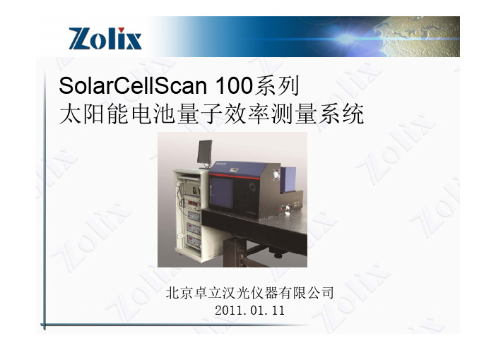
SolarCellScan 100系列 太阳能电池量子效率测量系统
北京卓立汉光仪器有限公司 2011.01.11
一.系统功能简介 二.系统性能 三.系统特点说明 四.其他专用机型简介
一. 系统功能简介
SolarCellScan 100是一款用于太阳能电池测试的实验平台。
可以实现测试太阳能电池的:光谱响应度、外量子效率、内 量子效率、反射率、表面均匀度、短路电流密度 等
上述Mapping数据是在同一个电池片上用400nm、650nm和950nm三个波 长做QE(LBIC)扫描得到的。650nm和950nm的扫描数据显示电池具有良好的 均匀性,但400nm扫描数据上,我们发现电池边缘有不均匀区域。
不同的测试波长对样品的穿透深度不同。蓝光波长短,穿透深度浅,因 此很容易将样品制备过程中产生的表面裂痕等问题反映出来;近红外光波长 相对较长,穿透深度更深,更加适用于扩散长度的计算,从而能反映样品材 料内部的缺陷等问题。
专业化样品夹持器
标准探针样品架30mm*30mm
真空吸附样品台,156mm*156mm
背电极薄膜样品架100mm*100mm
有机气密样品架,可充氮气放置样品老化
光电化学电池(PEC)专用附件
XY 电动调整台和Mapping功能
XY电动调整台适用于156mm*156mm 样品的扫描测试 QE均匀度扫描 反射率均匀度扫描 通过偏置光强改变扫描缺陷分布
肖特太阳能公司之太阳能技术和产品的发展[1]
![肖特太阳能公司之太阳能技术和产品的发展[1]](https://img.taocdn.com/s3/m/aa81fa0b79563c1ec5da713e.png)
Al / Ni
Advantages (优势):
1958 1980 1983 2002
applications (AEG)太阳能电池片应用于空间领域 Development work on thin film solar cells at MBB (a-Si) MBB对于薄膜电池片有进展 First shipments of glass tubes for solar thermal power plants (SCHOTT Rohrglas GmbH)
开始集热器系列产品规模化生产
2004 2005 2006 2007
JV Wacker SCHOTT Solar founded 成立 JV Wacker SCHOTT Solar 公司 Thin film production started in Jena 在 Jena生产薄膜组件 New sites set up in Spain and in the USA; existing sites expanded
大型系统 / 太阳能发电厂
© SCHOTT Solar AG
6
SCHOTT Solar AG
SNEC 3rd Solar (2009)at a glance SCHOTT
ASI® Products ASI 薄膜产品 Thin Film Amorphous ASI®
Framed modules 有框组件 • On-/Off-Grid 并网/离网 • 12 V applications 12V 应用
2
SCHOTT Solar AG
1 SNEC SCHOTT 3rd Solar (2009) Solar a glance SCHOTT atat a glance
钙钛矿太阳能电池英文缩写

钙钛矿太阳能电池英文缩写Perovskite Solar Cells: A Promising Technology for the Future of Photovoltaics.Perovskite solar cells have emerged as a promising technology for the future of photovoltaics due to their high efficiency, low cost, and ease of fabrication. Perovskite materials are a class of compounds with the general formula ABX3, where A and B are cations and X is an anion. In perovskite solar cells, the perovskite materialis used as the light-absorbing layer, and it is sandwiched between two electrodes. The most common type of perovskite material used in solar cells is methylammonium lead iodide (CH3NH3PbI3), but other perovskite materials are also being investigated.Perovskite solar cells have a number of advantages over traditional silicon solar cells. First, perovskite materials are much cheaper than silicon. Second, perovskite solar cells can be fabricated using solution-processingtechniques, which are much less expensive than the vacuum-deposition techniques used to fabricate silicon solar cells. Third, perovskite solar cells have a higher absorption coefficient than silicon, which means that they can be made thinner and lighter than silicon solar cells.The efficiency of perovskite solar cells has improved rapidly in recent years. In 2009, the best perovskite solar cells had an efficiency of just 3.8%. However, by 2018, the efficiency of perovskite solar cells had reached 25.2%, which is comparable to the efficiency of the best silicon solar cells.Perovskite solar cells are still in the early stages of development, but they have the potential to revolutionize the photovoltaic industry. Perovskite solar cells are cheaper, lighter, and more efficient than traditionalsilicon solar cells, and they can be fabricated using solution-processing techniques. These advantages make perovskite solar cells a promising technology for thefuture of photovoltaics.Here are some of the key challenges that need to be addressed before perovskite solar cells can be commercialized:Stability: Perovskite materials are sensitive to moisture and oxygen, and they can degrade over time. Researchers are working to develop more stable perovskite materials, but this is still a major challenge.Scalability: Perovskite solar cells are currently fabricated using small-scale solution-processing techniques. Researchers need to develop scalable manufacturing processes in order to produce perovskite solar cells at a commercial scale.Toxicity: Lead is a toxic metal, and it is present in the most common type of perovskite material used in solar cells. Researchers are working to develop lead-free perovskite materials, but this is still a challenge.Despite these challenges, perovskite solar cells havethe potential to revolutionize the photovoltaic industry.Perovskite solar cells are cheaper, lighter, and more efficient than traditional silicon solar cells, and they can be fabricated using solution-processing techniques. These advantages make perovskite solar cells a promising technology for the future of photovoltaics.。
硅BC8量子点太阳能电池中的多重激子效应
硅BC8量子点太阳能电池中的多重激子效应卢辉东;铁生年【摘要】多重激子效应是指在纳米半导体晶体中,量子点吸收一个高能光子而产生多个电子-空穴对的过程,该效应可以提高单结太阳电池能量转换效率.利用碰撞电离机制和费米统计模型计算了工作温度300 K的单结硅BC8量子点太阳能电池在AM1.5G太阳光谱下的能量转换效率.对于波长在280~580 nm的入射光,多重激子效应可以大幅增强硅BC8量子点直径d>5.0 nm的量子点太阳电池的能量转换效率.硅纳米量子点的直径d=6.3~6.4 nm时,最大能量转换效率为51.6%.%Multiple exciton generation( MEG) is a process whereby multiple electron-hole pairs or excitons are produced upon absorption of a single photon in semiconductor quantum dots ( QDs ) . This effect represents a promising route to increase solar conversion efficiencies in single-junction photovoltaic cells. MEG in Si BC8 QDs is based on impact ionization and statistical Fermi. The power conversion efficiency for Si QDs solar cells was calculated under AM1 . 5 G solar spectrum with the cell temperature at 300 K. For the incident wavelength of 280-580 nm, the power conversion efficiency can be improved by MEG effect for d>5. 0 nm Si QDs. For Si BC8 QDs with d=6. 3-6. 4 nm, the maximum energy conversion efficiency is 51. 6%.【期刊名称】《发光学报》【年(卷),期】2018(039)005【总页数】6页(P668-673)【关键词】多重激子效应;量子点;太阳能电池【作者】卢辉东;铁生年【作者单位】青海大学新能源光伏产业研究中心, 青海西宁 810016;青海大学新能源光伏产业研究中心, 青海西宁 810016【正文语种】中文【中图分类】O5211 引言多重激子效应(Multiple exciton generation,MEG)是指纳米尺度的半导体材料吸收一个能量等于或者大于二倍纳米半导体材料禁带宽度的光子而产生多个电激子的物理过程。
光伏行业英文词汇
太阳电池 solar cell通常是指将太阳光能直接转换成电能的一种器件。
硅太阳电池silicon solar cell硅太阳电池是以硅为基体材料的太阳电池。
单晶硅太阳电池single crystalline silicon solar cell单晶硅太阳电池是以单晶硅为基体材料的太阳电池。
非晶硅太阳电池〔a—si太阳电池〕amorphous silicon solar cell用非晶硅材料及其合金制造的太阳电池称为非晶硅太阳电池,亦称无定形硅太阳电池,简称a—si太阳电池。
多晶硅太阳电池polycrystalline silicon solar cell多晶硅太阳电池是以多晶硅为基体材料的太阳电池。
聚光太阳电池组件photovoltaic concentrator module系指组成聚光太阳电池,方阵的中间组合体,由聚光器、太阳电池、散热器、互连引线和壳体等组成。
电池温度cell temperature系指太阳电池中P-n结的温度。
太阳电池组件外表温度solar cell module surface temperature系指太阳电池组件背外表的温度。
大气质量〔AM〕Air Mass (AM)直射阳光光束透过大气层所通过的路程,以直射太阳光束从天顶到达海平面所通过的路程的倍数来表示。
太阳高度角solar太阳高度角solar elevation angle太阳光线与观测点处水平面的夹角,称为该观测点的太阳高度角。
辐照度irradiance系指照射到单位外表积上的辐射功率〔W/m2〕。
总辐照〔总的太阳辐照〕total irradiation (total insolation)在一段规定的时间内,〔根据具体情况而定为每小时,每天、每周、每月、每年〕照射到某个倾斜外表的单位面积上的太阳辐照。
直射辐照度direct irradiance照射到单位面积上的,来自太阳圆盘及其周围对照射点所张的圆锥半顶角为8o的天空辐射功率。
二氧化碳捕集技术发展现状
化学吸收法主要利用吸收剂的化学活性与 45" 发生化学反应!生成介稳化合物!然后改变外界条件 如温度(压力等!使生成物分解并释放 45" !达到捕 集 45" 的 目 的! 解 吸 后 的 吸 收 剂 可 以 再 循 环 使 用&&2' " 常用的 化 学 吸 收 剂 一 般 为 碱 性 液 体! 如 醇 胺(氨水和钾碱溶液等"
具有 45" 吸附功能的金属氧化物!一般为碱金 属或碱土金属类的氧化物!该类氧化物本身具有较 强的碱性!可以与 45" 发生化学反应!达到吸附的 目的" MOH 等人&&%' 制备的 J$PQ5A 金属氧化物吸 附材料!在 ,## 6(#7& 9:;的条件下!45" 的吸附 量为 #72"" <<=>8?" 金属氧化物及其盐类对 45" 的吸收能力较强!但是能耗较高!特别是 45" 脱附 过程!一般需要在 ,## R*## 6下进行!需要消耗大 量的能量"
第 ,' 卷!第 % 期 "#"' 年 % 月
绿色发展
煤气与热力
@+A BCD+(
E=>7,' F=7% GHI7"#"'
二氧化碳捕集技术发展现状
姜!鑫!金文龙!铁!宇
北京市燃气集团研究院 北京 &###&&
!!摘!要!二氧化碳捕集技术是未来碳减排的重要手段之一 综述了固体吸附法化学吸收法 和膜分离法 ' 种二氧化碳捕集技术的发展现状 固体吸附法的吸附剂主要包括碳类吸附材料沸 石金属类吸附材料化学吸收法的吸收剂主要包括醇胺类碳酸钾溶液氨水膜分离法常见的膜 有无机膜有机膜和复合膜 对各捕集技术的特点进行分析 !!关键词!二氧化碳捕集!固体吸附法!化学吸收法!膜分离法
太阳能电池用稀土铽掺杂二氧化硅减反射和光波转换薄膜
太阳能电池用稀土铽掺杂二氧化硅减反射和光波转换薄膜陈武军;王利明;冀若楠;郝媛媛;张宁宁;苗慧;孙倩;张德恺;胡晓云【摘要】采用凝胶溶胶法,在玻璃片上镀制了稀土铽掺杂的SiO2薄膜,讨论了稀土Tb3+和金属Zn2+掺杂及掺杂量对薄膜样品透过率曲线、发光和太阳能电池光电转换效率的影响.实验结果表明稀土Tb3+和金属Zn2+掺杂量均为0.4%时,薄膜样品的发光及太阳能输出功率最高,太阳能电池转换效率提高了6.25%.实现了减少反射和紫外可见光波转换的双重功能.【期刊名称】《西北大学学报(自然科学版)》【年(卷),期】2016(046)001【总页数】6页(P28-32,37)【关键词】太阳能电池;光电转换效率;光波转换;减反射膜【作者】陈武军;王利明;冀若楠;郝媛媛;张宁宁;苗慧;孙倩;张德恺;胡晓云【作者单位】西北大学物理学院,陕西西安710069;西北大学国家级光电技术与功能材料国际合作基地,陕西西安710069;西北大学物理学院,陕西西安710069;西北大学物理学院,陕西西安710069;西北大学物理学院,陕西西安710069;西北大学物理学院,陕西西安710069;西北大学物理学院,陕西西安710069;西北大学物理学院,陕西西安710069;西北大学物理学院,陕西西安710069;西北大学国家级光电技术与功能材料国际合作基地,陕西西安710069;西北大学物理学院,陕西西安710069;西北大学国家级光电技术与功能材料国际合作基地,陕西西安710069【正文语种】中文【中图分类】O484.4如今社会对能源的需求越来越大,而传统能源又不断地枯竭,致使可再生能源地位的日益提高。
太阳能作为可再生能源中的一大部分,备受关注。
但人类面对的问题是太阳能电池造价高昂并且光电转化效率较低。
因此,降低生产成本、提高光电转化效率是太阳能电池大规模实用化的前提[1-8]。
提高太阳能电池转换效率的方式有两种:一个是改进光电转换材料,另一个是改进组件。
- 1、下载文档前请自行甄别文档内容的完整性,平台不提供额外的编辑、内容补充、找答案等附加服务。
- 2、"仅部分预览"的文档,不可在线预览部分如存在完整性等问题,可反馈申请退款(可完整预览的文档不适用该条件!)。
- 3、如文档侵犯您的权益,请联系客服反馈,我们会尽快为您处理(人工客服工作时间:9:00-18:30)。
Screen printing POCl3 emitter diffusion PECVD SiNx
Co-firing Laser edge isolation
Laser coding Isotexture and wafer cleaning
DETAILED STUDY ON LARGE AREA 100% SOG SILICON MC SOLAR CELLS WITH EFFICIENCIES EXCEEDING 16%
A. Halm1, J. Jourdan1, S. Nichol2, B. Ryningen3, H. Tathgar3, R. Kopecek1
1International Solar Energy Research Center - ISC - Konstanz, Rudolf-Diesel-Str. 15, D-78467 Konstanz, Germany.
Phone : +49 7531-3618350 ; Fax: +49 7531-3618311 ; Email : Andreas.Halm@isc-konstanz.de 26N Silicon Inc., 1 Royal Gate Boulevard, Unit B, Vaughan Ontario, Canada L4L8Z7
3Umoe Solar AS, Fornebuveien 84, P.O. Box 60, 1324 Lysaker Norway
ABSTRACT: The focus of this work is the development and characterisation of 156x156 mm² sized industrial type screen printed silicon solar cells made of 100% solar grade silicon (SoG-Si). The feedstock under investigation is produced by 6N Silicon Inc. from metallurgical grade silicon with a lower cost low energy refining technique compared to the Siemens process. Solar cells were processed at ISC Konstanz with industrial type process equipment. Defining a stable baseline process at ISC Konstanz, the improvements of the 6N Silicon material achieved during one year were tested against a single polysilicon reference brick. In addition, process enhancements leading to higher efficiencies were investigated. Reaching the same average efficiency level for reference and 6N material applying the baseline process, an advanced process which still satisfies industrial production standards was defined. Running this advanced process achieved an average efficiency of 16.0% with 100% 6N Silicon feedstock, and a best cell having 16.3% efficiency. The four best cells of both materials and both processes are further characterised via SR, LBIC and thermography measurements to show material dependent characteristics on cell level. Reverse current behaviour and LID are tested for cells of different ingot positions which are relevant information for module manufacturers. Keywords: solar grade silicon feedstock, industrial solar cell process, cell characterisation
1 INTRODUCTION To satisfy the needs of the PV Industry, new solar grade silicon feedstocks are being designed to achieve lower cost levels while having higher impurities as compared to polysilicon feedstock that has been designed for the semiconductor industry. Multicrystalline solar cells made of solar grade silicon have a high potential for future green energy production, particularly as they can be manufactured at lower cost levels. SoG-Si producers like 6N Silicon Inc., Dow Corning, Timminco, or Globe emphasize the leading role of North America in this emerging sector of the PV industry. Satisfying the lower purity requirements for silicon specially made for PV applications, new refining techniques which are more basic and less energy intensive as the Siemens process are explored. This is beneficial for module prices and for energy payback time when similar efficiencies can be reached on SoG-Si compared to polysilicon [1]. Though some performance disparities were reported in the past, SoG-Si is now evolving towards the criteria set by industrial cell and module manufacturers. We have produced industrial type screen printed solar cells with efficiencies higher than 16% using 100% 6N Silicon SoG-Si. We have shown that for both processes applied at ISC the performance of cells made of the 100% 6N Silicon material is comparable to the reference cells made from polysilicon produced with the same process at the same time. We have performed detailed characterization to identify different properties of these two species of solar cells. 2 EXPERIMENTAL 2.1 Solar grade silicon 6N Silicon Inc. has developed a low temperature purification process for silicon through Al-Si melt segregation. The aluminium content of the feedstock end product, however, was observed to be lower than 0.05 ppmw. The overall contamination levels are sufficiently low to meet the needs of a solar cell producer. For the purpose of this study the feedstock was processed into multicrystalline silicon ingots with bulk resistivities between 0.4-2.7 Ωcm. A detailed description of the material purification process and the properties of the grown mc SoG ingots was already provided in [2].
2.2 Solar cell process To be able to monitor changes in material quality over a long period of time, a stable baseline process is defined at ISC Konstanz. At the same time one brick with