电阻率参杂计算
常用导体材料电阻率计算公式
常用导体材料电阻率计算公式Company Document number:WTUT-WT88Y-W8BBGB-BWYTT-19998【电学部分】1电流强度:I=Q电量/t2电阻:R=ρL/S3欧姆定律:I=U/R4焦耳定律:⑴Q=I2Rt普适公式)⑵Q=UIt=Pt=UQ电量=U2t/R (纯电阻公式) 5串联电路:⑴I=I1=I2⑵U=U1+U2⑶R=R1+R2⑷U1/U2=R1/R2 (分压公式)⑸P1/P2=R1/R26并联电路:⑴I=I1+I2⑵U=U1=U2⑶1/R=1/R1+1/R2 [ R=R1R2/(R1+R2)]⑷I1/I2=R2/R1(分流公式)⑸P1/P2=R2/R17定值电阻:⑴I1/I2=U1/U2⑵P1/P2=I12/I22⑶P1/P2=U12/U228电功:⑴W=UIt=Pt=UQ (普适公式)⑵W=I^2Rt=U^2t/R (纯电阻公式)9电功率:⑴P=W/t=UI (普适公式)⑵P=I2^R=U^2/R (纯电阻公式)电流密度的问题:一般说铜线的电流密度取6A/mm2,铝的取4A,考虑到大电流的趋肤效应,越大的电流取的越小一些,100A以上一般只能取到左右,另外还要考虑输电线路的线损,越长取的也要越小一些。
计算所有关于电流,电压,电阻,功率的计算公式1、串联电路电流和电压有以下几个规律:(如:R1,R2串联)①电流:I=I1=I2(串联电路中各处的电流相等)②电压:U=U1+U2(总电压等于各处电压之和)③电阻:R=R1+R2(总电阻等于各电阻之和)如果n个阻值相同的电阻串联,则有R总=nR2、并联电路电流和电压有以下几个规律:(如:R1,R2并联)①电流:I=I1+I2(干路电流等于各支路电流之和)②电压:U=U1=U2(干路电压等于各支路电压)③电阻:(总电阻的倒数等于各并联电阻的倒数和)或。
如果n个阻值相同的电阻并联,则有R总= R注意:并联电路的总电阻比任何一个支路电阻都小。
电阻率计算公式
电阻率计算公式。
电阻率是描述导体的电阻的量度值,它常常被称为抗拒率。
电阻率是一个物理概念,它表示导体对电流的抗力,也就是电流流过导体时产生的力矩。
电阻率计算公式R = ρ/A,其
中R表示电阻率,ρ表示实质密度,A表示横截面积。
电阻率计算公式非常重要,它可以帮助我们知道不同导体在相同条件下电流在导体中流通时产生的力矩大小。
电阻率又称抗拒率,反映的就是当电流流过一个导体时,它想要克服的电动势的大小。
因此,电阻率的大小取决于材料的实质性质和横截面积:其实质越大,
横截面积越小,电阻率就越大,反之亦然。
因此,要想做出高电阻率的电路元件来满足特
定应用需求,就要选择实质密度大、横截面积小的材料来生产元件。
电阻率的计算是物理、电气以及电子技术的一个重要部分,它用来确定电路中的动态行为,从而可以确定在电路中电动势强度及其他参数。
本公式的应用非常广泛,从工业电气控制
到家庭用电,所有的电气设备都需要这个公式来工作。
电阻率对于导体类型的挑选也非常
有帮助,它可以帮助我们找到特定应用需求最佳的电路材料。
配料电阻率计算公式

0.0012 0.0012 0.0012
9.70E+19 9.70E+19 9.70E+19 母合金掺加合计 掺杂剂
0.00E+00 0.00E+00 0.00E+00 0.00E+00 掺入母合金重量
掺杂剂电阻率 0.0012 0.0012 0.0012 0.0012 0.0012 0.00Байду номын сангаас2 0.0012 0.0012
掺杂剂浓度 9.70E+19 9.70E+19 9.70E+19 9.70E+19 9.70E+19 9.70E+19 9.70E+19 9.70E+19 母合金掺加合计 0.00 0.00E+00 0.00E+00 0.00E+00 0.00E+00 0.00E+00 0.00E+00 0.00E+00 0.00E+00
1.使用P 型料生产单晶计算
P 型料投料情况 投料类型 原始多晶 3.5 0.8 P 型边皮,头尾,棒料 1.7 2.5 1.2 4.5 投料量合计 P 型料投料情况 投料类型 原始多晶 3.5 0.9 P 型边皮,头尾,棒料 1.8 2.5 1.3 4.5 投料量合计 P 型料投料情况 投料类型 原始多晶 0.9 0.8 1.2 1.3 P 型边皮,头尾,棒料 1.7 1.8 3.5 8.24E+15 7.76E+15 3.89E+15 1.9 1.9 1.9 7.33E+15 7.33E+15 7.33E+15 1.64E+16 1.87E+16 1.20E+16 1.10E+16 投入量 平均电阻率 浓度 0 目标电阻率及浓度 目标电阻率 1.7 1.9 1.9 1.9 1.9 目标电阻率浓度 8.24E+15 7.33E+15 7.33E+15 7.33E+15 7.33E+15 3.89E+15 1.64E+16 7.76E+15 5.51E+15 1.10E+16 3.01E+15 投入量 平均电阻率 浓度 0 目标电阻率及浓度 目标电阻率 1.6 1.6 1.6 1.6 1.6 1.6 1.6 目标电阻率浓度 8.79E+15 8.79E+15 8.79E+15 8.79E+15 8.79E+15 8.79E+15 8.79E+15 3.89E+15 1.87E+16 8.24E+15 5.51E+15 1.20E+16 3.01E+15 投入量 平均电阻率 浓度 目标电阻率及浓度 目标电阻率 1.7 1.7 1.9 1.9 1.7 1.9 1.7 目标电阻率浓度 8.24E+15 8.24E+15 7.33E+15 7.33E+15 8.24E+15 7.33E+15 8.24E+15
掺杂浓度与电阻率关系
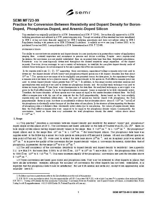
SEMI MF723-99Practice for Conversion Between Resistivity and Dopant Density for Boron-Doped, Phosphorus-Doped, and Arsenic-Doped SiliconThis standard was originally published by ASTM International as ASTM F 723-81. It was formally approved by ASTMballoting procedures and adhered to ASTM patent requirements. Though ownership of this standard has been transferredto SEMI, it has not been formally approved by SEMI balloting procedures and does not adhere either to SEMIRegulations dealing with patents or to SEMI Editorial Guidelines. Available at October 2003, to bepublished November 2003. Last published by ASTM International as ASTM F 723-99.INTRODUCTIONThe ability to convert between resistivity and dopant density in a semiconductor is important for a variety of applicationsranging from material inspection and acceptance to process and device modeling. Despite some experimentallimitations, the conversion is more readily established from an empirical data base than from theoretical calculations.Resistivity may be unambiguously determined throughout the desired resistivity range regardless of the dopantimpurity. However, it was necessary to use a variety of techniques to establish the complete dopant density scale ofinterest; these techniques do not all respond to the same parameter of the semiconductor.In the experimental work (1), (2), (3)1 supporting these conversions, capacitance-voltage measurements were used todetermine the dopant density of both boron- and phosphorous-doped specimens with dopant densities less than about1018 cm−3. The specimens were assumed to be negligibly compensated; hence, the data given by the capacitance-voltagemeasurements were taken to be a direct measure of the dopant density in the specimen. Hall effect measurements wereused to obtain dopant density values greater than 1018 cm−3. In addition, in this range neutron activation analysis andspectrophotometric analysis were used to determine phosphorus density, and the nuclear track technique was used todetermine boron density. Where there were discrepancies in the data from the analytical techniques, more weight wasgiven to the Hall effect results. Up to the highest densities measured, boron is expected to be fully electrically active.Therefore, the boron densities of these specimens were assumed equal to the carrier densities obtained from the Halleffect measurements with the use of an estimate for the Hall proportionality factor based on the best availableexperimental and theoretical information. In the case of specimens heavily doped with phosphorus, the Hallproportionality factor is unity, but there is considerable evidence that at densities above about 5 × 1019 cm−3 not all ofthe phosphorus is electrically active because of the formation of complexes. In the absence of data regarding the fractionof phosphorus atoms withdrawn from electrically active states due to complexing, the values of carrier density takenfrom the Hall effect measurements were assumed to be equal to the phosphorus density values. Consequently, theconversions based on these data may understate the total phosphorus density for stated values above about5 × 1019 cm−3.1. Scope1.1 This practice 2 describes a conversion between dopant density and resistivity for arsenic-, boron- and phosphorus-doped single crystal silicon at 23°C. The conversions are based primarily on the data of Thurber et al (1), (2), (3)2 taken on bulk single crystal silicon having dopant density values in the range from 3 × 1013 cm−3 to 1 × 1020 cm−3 for phosphorus-doped silicon and in the range from 1014 cm−3 to 1 × 1020 cm−3 for boron-doped silicon. The phosphorus data base was supplemented in the following manner: two bulk specimen data points of Esaki and Miyahara (4) and one diffused specimen data point of Fair and Tsai (5) were used to extend the data base above 1020cm−3, and an imaginary point was added at 1012 cm−3 to improve the quality of the conversion for low dopant density values. A conversion for arsenic, distint from that of phosphorus, is presented for the range 1019 to 6 by 1020cm−3.1.2 The self consistency of the conversion (resistivity to dopant density and dopant density to resistivity) (see Appendix X1) is within 3 % for boron from 0.0001 to 10 000 Ω·cm, (10 12 to 1021 cm−3) and within 4.5 % for phosphorus from 0.0002 to 4000 Ω·cm (1012 to 5 × 10 20cm−3). This error increases rapidly if the phosphorus conversions are used for densities above 5 × 1020 cm−3 .1.3 These conversions are based upon boron and phosphorus data. They may be extended to other dopants in silicon that have similar activation energies; although the accuracy of conversions for other dopants has not been established, it is expected that the phosphorus data would be satisfactory for use with arsenic and antimony, except when approaching solid solubility (see 6.3).1 Boldface numbers in parentheses refer to the list of references at the end of this practice.2 DIN 50434 is an equivalent method. It is the responsibility of DIN Committee NMP 221, with which Comittee F-1 maintains close technical liaison. DIN 50444, Testing of Materials for Semiconductor Technology: Conversion Between Resistivity and Dopant Density of Silicon, is available from Beuth Verlag GmbH Burggrafenstrasse 4-10, D-1000 Berlin 30, Federal Republic of Germany.1.4 These conversions are between resistivity and dopant density and should not be confused with conversions between resistivity and carrier density or with mobility relations.N OTE 1—The commonly used conversion between resistivity and dopant density compiled by Irvin (6) is compared with this conversion in Appendix X2. In this compilation, Irvin used the term “impurity concentration” instead of the term “dopant density.”1.5 This standard does not purport to address all of the safety concerns, if any, associated with its use. It is the responsibility of the user of this standard to establish appropriate safety and health practices and determine the applicability of regulatory limitations prior to use.2. Referenced Documents2.1 ASTM Standards:F 84 Test Method for Measuring Resistivity of Silicon Wafers with an In-Line Four-Point Probe 32.2 Adjuncts:Large Wall Chart 43. Terminology3.1 Definitions:3.1.1 carrier density, n (electrons);p (holes)—the number of majority carriers per unit volume in an extrinsic semiconductor, usually given in number/cm 3 although the SI unit is number/m3.3.1.2 compensation—reduction in number of free carriers resulting from the presence of impurities other than the majority dopant density impurity. Compensation occurs when both donor and acceptor dopant impurities are present in a semiconductor; in this case the net dopant density (which is equal to the carrier density provided that all the dopant impurities are ionized) is given by the absolute magnitude of the difference between the acceptor dopant density and the donor dopant density. Compensation may also occur if deep-level impurities or defects are present in quantities comparable with the dopant impurities; in this case the relationship between the carrier density and the dopant density (under the assumption of full ionization of the dopant impurity) depends on a variety of parameters (7). A semiconductor that exhibits compensation is said to be “compensated.”3.1.3 concentration—relative amount of a minority constituent of a mixture to the majority constituent (for example, parts per million, parts per billion, or percent) by either volume or weight. In the semiconductor literature, often used interchangeably with number density (for example, number per unit volume).3.1.4 deep-level impurity—a chemical element that when introduced into a semiconductor has an energy level (or levels) that lies in the mid-range of the forbidden energy gap, between those of the dopant impurity species.3.1.4.1 Discussion-Certain crystal defects and complexes may also introduce electrically active deep levels in the semiconductor.3.1.5 dopant density—in an uncompensated extrinsic semiconductor, the number of dopant impurity atoms per unit volume, usually given in atoms/cm3 although the SI unit is atoms/m3. Symbols: N D for donor impurities and N A for acceptor impurities.4. Summary of Practices4.1 The conversions between resistivity and dopant density are made using equations, tables, or graphs.5. Significance and Use5.1 Dopant density and resistivity of silicon are two important acceptance parameters used in the interchange of material by consumers and producers in the semiconductor industry. Therefore, a particular method of converting from dopant density to resistivity and vice versa must be available since some test methods measure resistivity while others measure dopant density.5.2 These conversions are useful in mathematical modeling of semiconductor processing and devices.3 Annual Book of ASTM Standards, Vol 10.05, ASTM International, 100 Barr Harbor Drive, West Conshohocken, PA 19428. Telephone: 610-832-9500, Fax: 610-832-9555, Website: 4 A large wall chart, “Conversion Between Resistivity and Dopant Density” is available from ASTM, 100 Barr Harbor Drive, West Conshohocken, PA 19428. Order Adjunct ADJF0723.6. Interferences6.1 Carrier Density— Attempts to derive carrier density values from resistivity values by using these conversions are subject to error. While dopant density and carrier density values are expected to be the same at low densities (up to about 1017 cm−3), the two quantities generally do not have the same value in a given specimen at moderate densities. At such moderate densities, (about 1017 cm−3 to 1019 cm−3), dopant densities are larger than carrier densities due to incomplete ionization. At densities above 10 19 cm−3, the population statistics become degenerate, and carrier densities would normally be equal to dopant densities. However, in this upper range of densities, the possibility of formation of compounds or complexes involving dopant atoms is more pronounced and would prevent some of the dopant atoms from being electrically active. Such formation of compounds or complexes is particularly likely in phosphorus- or arsenic-doped silicon. Precipitation occurs at dopant densities greater than solid solubility.6.2 Heavily Phosphorus-Doped Silicon—These conversions are given as functions of resistivity and of dopant density. For heavily phosphorus-doped specimens, primary emphasis was placed on Hall effect measurements for establishing the density values. However, since the Hall effect measures carrier density, it was assumed for these heavily doped specimens that all atoms were electrically active; that is, the dopant density was equal to the carrier density as measured by the Hall effect. The possible formation of phosphorus-vacancy pairs which are known to reduce the electrically active phosphorus atoms at high densities (5) was not tested or accounted for in the data base or the resulting conversions. The existence of such phosphorus-vacancy pairs would cause the Hall measurements to understate the total dopant density for the heavily phosphorus-doped specimens.6.3 Other Dopant Species—The applicability of these conversions to silicon doped with other than arsenic, boron or phosphorus has not yet been established. However, in the lightly doped range (<1017 cm−3) the conversions are expected to be reasonably accurate for other dopants. Between 10 17 and 1019 cm −3, the difference in activation energy of different dopant species will cause different resistivities to be measured for the same dopant density. In this range the differences in resistivities will be larger among the p-type dopants than among the n-type dopants due to larger differences in the activation energies among the p-type dopants. At high dopant densities (>1019 cm−3), the formation of complexes involving dopant atoms, lattice defects, and other impurities will lead to a modification in the number of charge carriers. The extent of this effect will depend upon the particular dopant species and is not well detailed in the literature for the various common dopants. Its onset is expected to be related to the density of the dopant compared to the solid solubility of that dopant in silicon. Therefore, in this upper dopant density range, the applicability of these conversions to dopants other than boron and phosphorus is unclear.6.4 Compensation— The specimens used to obtain the data base for these conversions were assumed to be uncompensated. The measured net dopant density was taken to be the total density of the intentional dopant in the specimen. For specimens in which significant compensation occurs, these conversions may not apply.6.5 Temperature— The conversions in this practice hold for a temperature of 23°C. Resistivity varies with temperature, but dopant density does not.N OTE 2—It is possible to obtain dopant density values from resistivity values that were not measured at 23°C by using Test Method F 84 to correct the resistivity values to 23°C. Also, the conversion from dopant density to resistivity may be made directly and the temperature correction for resistivity then made following Test Method F 84 to obtain the resistivity at other than 23°C.N OTE 3—References 1, 2, and 3 give values for the coefficients in the conversion equations at both 23°C and 300 K.6.6 Other Electrically Active Centers—Numerous other mechanisms exist that may modify the number of free carriers or noticeably alter carrier mobility, either of which will change the resistivity from the value given here for a given dopant density. Among these mechanisms are (1) lattice damage due to radiation (neutron transmutation doping or ion implantation), (2) formation of deep level centers due to chemical impurities (typically heavy metals, either unwanted or sometimes intentionally added for minority carrier lifetime control), and (3) unintentional doping due, for example, to electrically activated oxygen. When any of these effects is known or expected to be present, the conversions given here may not apply.6.7 Range of Arsenic-Doped Silicon Data—The conversion given for arsenic-doped silicon is from Fair and Tsai (8), covering the doping range of 1019 to 6 by 1020. This conversion was generated using Hall effect measurements. The principal reference for neutron activation data is that of Newman et al.(9). Neutron activation data give higher resistivity values for a given dopant density than do Hall data because of the assumption that the Hall coefficient R H = 1/ne. A more complicated relationship between R H and n is given in Ref (9). Care must be taken in using any conversion not to extrapolate beyond the range of the data fitted, as the formulas will diverge beyond that range. Other studies support the use of the conversion given here Refs (10, 11, 12, and 13), which means that the conversion to resistivity for phosphorus can be used for arsenic in this range. In the range 2 by 1019 to 1020, the Fair and Tsai fit matches the Irvin formula. The range beyond 6 by 1020 is discussed only in Ref (13).7. Procedure7.1 Convert Resistivity Values to Dopant Density Values— Follow 7.1.1 (graphical method), 7.1.2 (tabular method), or 7.1.3 (computation method). 57.1.1 Graphical Method:7.1.1.1 For boron-doped silicon, use the curve labeled “boron” in Fig. 1.7.1.1.2 For phosphorus-doped silicon, use the curve labeled “phosphorus” in Fig. 1.7.1.2 Tabular Method:7.1.2.1 For boron-doped silicon use Table 1.TABLE 1 Dopant Density as a Function of Resistivity for Boron-Doped SiliconN OTE 1—Entries in two significant digits are for regions of extrapolated data.TABLE 1 Continued7.1.2.2 For phosphorus-doped silicon use Table 2.7.1.3 Computational Method :7.1.3.1 For boron-doped silicon, calculate the dopant density value from the resistivity value as follows:N = 1.330 × 10 16ρ + 1.082 × 10 17ρ []1 + ()54.56ρ 1.105 (1)where:ρ= resistivity and N = dopant density.7.1.3.2 For phosphorus-doped silicon, calculate the dopant density from the resistivity as follows:N = 6.242 × 10 18ρ × 10 Z (2)where:Z = A 0 + A 1x + A 2x 2 + A 3x 31 + B 1x + B 2x2 + B 3x3 (3)where:x = log 10ρ,A 0 = −3.1083,A1 =−3.2626,A2 =−1.2196,A3 =−0.13923,B 1= 1.0265,B2= 0.38755, andB3= 0.041833.7.2 Convert Dopant Density Values to Resistivity Values—Follow 7.2.1 (graphical method), 7.2.2 (tabular method), or 7.2.3 (computational method).TABLE 2 Dopant Density as a Function of Resistivity for Phosphorus-Doped SiliconN OTE 1—Entries in two significant digits are for regions of extrapolated data.TABLE 2 Continued7.2.1 Graphical Method:7.2.1.1 For boron-doped silicon, use the curve labeled “boron” in Fig. 1.7.2.1.2 For phosphorus-doped silicon, use the curve labeled “phosphorus” in Fig. 1.7.2.2 Tabular Method:7.2.2.1 For boron-doped silicon, use Table 3.TABLE 3 Resistivity as a Function of Dopant Density for Boron-Doped Silicon N OTE 1—Entries in two significant digits are for regions of extrapolated data.TABLE 3 Continued7.2.2.2 For phosphorus-doped silicon, use Table 4.7.2.3 Computational Method :7.2.3.1 For boron-doped silicon, calculate the resistivity from the dopant density as follows:ρ = 1.305 × 10 16N + 1.133 × 10 17N []1 + ()2.58 × 10 −19 N −0.737(4) 7.2.3.2 For phosphorus-doped silicon, calculate the resistivity from the dopant density as follows: ρ = 6.242 × 10 18N × 10 Z (5)where:Z = A 0 + A 1y + A 2y 2 + A 3y 31 + B 1y + B 2y2 + B 3y3 (6)where:y = (log 10N ) − 16,A 0 = −3.0769,A 1 = 2.2108,A 2 = −0.62272,A 3 = 0.057501,B 1 = −0.68157,B 2 = 0.19833, andB3 =−0.018376.7.2.3.3 For arsenic-doped silicon, calculate the resistivity from the dopant density as follows:log10ρ = −6633.667 + AX + BX2 + CX3 + DX 4 + EX5 + FX6 + GX 7 + HX8 + IX9 + JX 10(7) where:log10N,X =768.2531,A =B =−25.77373,C= 0.9658177,D =−0.05643443,E =−8.008543 × 10 −4,F =9.055838 × 10 −5,G =−1.776701 × 10 −6,H =1.953279 × 10 −7,I =−5.754599 × 10 −9, andJ =−1.31657 × 10 −11.SEMI MF723-99 © SEMI 200311TABLE 4 Resistivity as a Function of Dopant Density for Phosphorus-Doped SiliconN OTE1—Entries in two significant digits are for regions of extrapolated data.SEMI MF723-99 © SEMI 2003 12TABLE 4 Continued8. Keywords8.1 arsenic; boron; dopant density; phosphorus; resistivity; siliconSEMI MF723-99 © SEMI 200313N OTE 1—The solid line shows the resistivity to dopant density conversion for the range of actual data. The chain dot line showsthe dopant density to resistivity conversion for the range of actual data. Dashed lines show regions of extrapolation from data.N OTE 2—On the scale of the figure as reproduced in this book, the solid and chaindot lines cannot be distinguished visually. Theyare distinguishable, however, on the wall chart available as Adjunct PCN 12-607230-46, wherever the self-consistency error (seeAppendix X1) becomes appreciable.FIG. 1 Preferred Conversion Between Resistivity and Total Dopant Density Values for Boron- and Phosphorus-Doped SiliconSEMI MF723-99 © SEMI 2003 14APPENDIXES(Nonmandatory Information)X1. DIFFERENCES IN CONVERSION SCALES ENCOUNTERED WHEN USING THE TABULAR ORCOMPUTATIONAL FORMS OF THIS PRACTICEX1.1 The conversion equations and the resulting tables are derived by fitting the experimental data using either resistivity or dopant density as the independent variables. This leads to complementary equations, for example, 7.1.3.1 and 7.2.3.1. These complementary equations are not exactly equivalent mathematically and small discrepancies can be found when using the equations or the tables derived from them. A given value of resistivity (for example, 1.00Ω· cm p -type) would convert to a dopant density value (1.46 × 1016cm −3), but the use of that dopant density in the complementary equation (or table) gives a resistivity (1.02 Ω·cm) which is different from the starting value. In this case, there is a 2 % (1.00 Ω·cm versus 1.02 Ω·cm) self-consistency error.X1.2 The self-consistency errors are plotted in Fig. X1.1.SEMI MF723-99 © SEMI 200315FIG. X1.1 Differences in Conversion Scales Encountered When Using this PracticeSEMI MF723-99 © SEMI 200316FIG. X1.2 Comparison of Conversions Between Resistivity and Dopant Density with Those of IrvinX2. COMPARISON OF CONVERSIONS WITH THOSE DUE TO IRVINX2.1 Irvin (6) reported conversion relations between resistivity and dopant density for n - and p -type silicon at 300 K. Irvin chose to use the term impurity concentration instead of the term dopant density. Irvin's analysis was based on a compilation of data by other authors based on several donor and acceptor dopants of similar energy levels in the silicon band gap and was supplemented by data taken by Irvin on heavily arsenic- and boron-doped specimens. All specimens were assumed to be uncompensated, but the possibility of compensation because of thermal activation of oxygen in the Czochralski crystals was recognized.X2.2 A comparison of the conversions given by this method with those due to Irvin is shown in Fig. X1.2.SEMI MF723-99 © SEMI 2003 17REFERENCES(1) Thurber, W. R., Mattis, R. L., Liu, Y. M., and Filliben, J. J., “Resistivity-Dopant Density Relationship for Phosphorus-Doped Silicon,” Journal of the Electrochemical Society , Vol 127, 1980, pp. 1807–1812.(2) Thurber, W. R., Mattis, R. L., Liu, Y. M., and Filliben, J. J., “Resistivity-Dopant Density Relationship for Boron-DopedSilicon,” Journal of the Electrochemical Society , Vol 127, 1980, pp. 2291–2294.(3) Thurber, W. R., Mattis, R. L., Liu, Y. M., and Filliben, J. J., Semiconductor Measurement Technology ,“ RelationshipBetween Resistivity and Dopant Density for Phosphorus- and Boron-Doped Silicon,” NBS Special Publication 400-64 (April 1981).(4) Esaki, L., and Miyahara, Y., “A New Device Using the Tunneling Process in Narrow p-n Junction,” Solid-StateElectronics , Vol 1, 1960, pp. 13–21.(5) Fair, R. B., and Tsai, J. C. C., “A Quantitative Model for the Diffusing of Phosphorus in Silicon and the Emitter DipEffect,” Journal of the Electrochemical Society, Vol 124, 1977, pp. 1107–1118.(6) Irvin, J. C.,“ Resistivity of Bulk Silicon and of Diffused Layers in Silicon,” Bell System Technical Journal, Vol 41, 1962,pp. 387–410.(7) Blakemore, J. S., Semiconductor Statistics, Pergamon Press, Oxford, 1962, pp. 153–161.(8) Fair, R. B., and Tsai, J. C. C., “The Diffusion of Ion-Implanted Arsenic in Silicon,” Journal of the ElectrochemicalSociety, Vol 122, No. 12, l975, p. 1689.(9) Newman, P. F., Hirsch, M. J., and Holcomb, D. F., “A Calibration Curve for Room-Temperature Resistivity versusDonor Atom Concentration in Si:As,” Journal of Applied Physics, Vol 58, No. 10, l985, p. 3779.(10) Furukawa, Y., “Impurity Effect Upon Mobility in Heavily Doped Silicon,” Journal of Physics Society, Japan, Vol 16,l961, p. 577.(11) Murota, J., Arai, E., Kobayashi, K., and Kudo, K., “Relationship Between Total Arsenic and Electrically Active ArsenicConcentrations in Silicon Produced by the Diffusion Process.” Journal of Applied Physics, Vol 50, No. 2, l979, p. 804.(12) Matsumoto, S., Niimi, T., Murota, J., and Arai, E., “Carrier Concentration and Hall Mobility in Heavily Arsenic-DiffusedSilicon,” Journal of Electrochemical Society, Vol 127, No. 7, l980, p. 1650.(13) Masetti, G., Severi, M., and Solmi, S., “Modeling of Carrier Mobility Against Carrier Concentration in Arsenic-,Phosphorus-, and Boron-Doped Silicon,” IEEE Trans. on Elec. Dev., ED-30, No. 7, l983, p. 764.NOTICE: SEMI makes no warranties or representations as to the suitability of the standards set forth herein for any particular application. The determination of the suitability of the standard is solely the responsibility of the user. Users are cautioned to refer to manufacturer's instructions, product labels, product data sheets, and other relevant literature, respecting any materials or equipment mentioned herein. These standards are subject to change without notice.By publication of this standard, Semiconductor Equipment and Materials International (SEMI) takes no position respecting the validity of any patent rights or copyrights asserted in connection with any items mentioned in this standard. Users of this standard are expressly advised that determination of any such patent rights or copyrights, and the risk of infringement of such rights are entirely their own responsibility.Copyright by SEMI® (Semiconductor Equipment and MaterialsInternational), 3081 Zanker Road, San Jose, CA 95134. Reproduction ofthe contents in whole or in part is forbidden without express writtenconsent of SEMI.。
电阻率的公式

电阻率的公式
电阻率是一种重要的物理量,它是物理学家研究物体对电流的阻力大小的一个量度。
一般来说,电阻率等于电压除以电流,表达公式如下:
R=V/I
R表示电阻率,V表示电压,I表示电流。
电阻率的单位是欧姆(Ω)。
电阻率也可以通过振荡电路的公式来表示:
R=sqrt(L/C)
其中,L表示振荡电路中的感觉电感,C表示振荡电路中的电容量。
电阻率的单位是欧姆,也就是说,如果电压为1伏特,电流为1安培,那么电阻率就是1欧姆。
在实际应用中,电阻率受到许多因素的影响,如环境温度、压力、电解质溶液的浓度等。
电阻率的变化反映在电器产品中,如电阻、电容、电感等。
因此,对于电子产品来说,很重要的是要测量电阻率,以便确保产品的可靠性和安全性。
一般来说,在设计电子产品时,都会将各种元件的电阻率进行检测和测量,只有电阻率符合要求,才能让器件发挥最佳性能。
此外,电阻率也可用于测量液体的粘度、气体的粘度以及物质的流动性能。
比如液体的粘度可以通过电阻率来测量,气体的粘度也可
以通过电阻率来测量。
总之,电阻率是一种重要的物理概念,它通过电压、电流和振荡电路的公式可以被表达出来。
它的应用非常广泛,可以用来检测和测量电子产品的可靠性,也可以用来测量液体和气体的粘度以及物质的流动性能。
电阻率可以为我们提供重要的物理参数,从而帮助我们更好地理解物体的物理性质。
电阻率作业指导书
电阻率作业指导书一、任务背景电阻率是描述材料导电性能的重要指标,它反映了单位长度和单位截面积的材料内部电阻的大小。
在工程和科学领域中,电阻率的准确测量对于材料的选择和设计具有重要意义。
本次作业旨在匡助学生了解电阻率的概念、测量方法以及应用。
二、电阻率的概念和计算公式电阻率(ρ)是指单位长度和单位截面积的材料内部电阻的大小。
它可以通过以下公式计算得出:ρ = R × (A/L)其中,ρ为电阻率,R为电阻,A为截面积,L为长度。
三、电阻率的测量方法1. 四引线法四引线法是一种常用的测量电阻率的方法,它可以排除导线电阻对测量结果的影响。
具体步骤如下:(1)准备一个标准电阻,测量其电阻值,记作R0。
(2)将待测材料样品的两端分别与电源和电流表相连,形成电路。
(3)记录电流表的读数I和电源的电压V。
(4)根据欧姆定律计算电阻值R = V/I。
(5)计算电阻率ρ = R × (A/L)。
2. 桥式法桥式法是另一种常用的测量电阻率的方法,它利用电桥平衡原理进行测量。
具体步骤如下:(1)搭建电桥电路,其中包括待测材料样品、标准电阻、电源和电流表。
(2)调节电桥的平衡,使得电流表读数为零。
(3)记录电源的电压V和标准电阻的电阻值R0。
(4)根据欧姆定律计算待测材料样品的电阻值R = V/R0。
(5)计算电阻率ρ = R × (A/L)。
四、电阻率的应用电阻率在工程和科学领域有广泛的应用,以下是几个例子:1. 材料选择:电阻率可以用来评估材料的导电性能,从而在设计过程中选择合适的材料。
2. 电子元件设计:电阻率可以用来计算电阻元件的尺寸,确保电路的正常工作。
3. 电力传输:电阻率可以用来评估输电路线的电阻损耗,优化电力传输效率。
五、实验操作注意事项1. 实验过程中要注意安全,遵守实验室操作规范。
2. 选择合适的测量方法,根据实际情况进行选择。
3. 在进行测量时,确保电路连接稳定,排除外部干扰。
电阻率作业指导书

电阻率作业指导书一、引言电阻率是材料的基本物理性质之一,用来描述材料对电流流动的阻碍程度。
在电路设计和材料研究中,电阻率的准确测量对于分析材料的导电性能和优化电路设计至关重要。
本指导书旨在提供关于电阻率测量的详细步骤和准确测量的方法。
二、背景知识1. 电阻率的定义:电阻率(ρ)是指单位长度和单位横截面积的材料对电流的阻力。
单位为欧姆·米(Ω·m)。
2. 电阻率的计算公式:电阻率可以通过以下公式计算得出:ρ = R × (A/L)其中,ρ为电阻率,R为电阻,A为截面积,L为长度。
三、实验步骤1. 准备工作:a. 确保实验室环境安全,仪器设备正常工作。
b. 准备所需材料和仪器:电阻测量仪、导线、电流源、电压表等。
c. 检查仪器的精度和校准状态,确保测量结果的准确性。
2. 选择适当的材料:根据实验要求和目的,选择适当的材料进行电阻率测量。
常见的材料包括金属、合金、导体、半导体等。
3. 准备样品:a. 根据实验要求,制备适当尺寸和形状的样品。
b. 确保样品表面光滑、清洁,避免污染和氧化对测量结果的影响。
4. 连接电路:a. 将电流源和电压表连接到电路中,确保电路的正常工作。
b. 使用导线将电流源、电压表与样品连接起来,确保连接牢固、无松动。
5. 测量电阻:a. 设置电流源的电流大小,一般选择适中的数值。
b. 使用电阻测量仪测量电路中的总电阻。
c. 记录测量结果,并计算出电阻率。
6. 数据分析:a. 根据测量结果计算出样品的电阻率。
b. 对测量结果进行统计分析,计算平均值和标准偏差,评估测量的准确性和可靠性。
7. 结果和讨论:a. 将测量结果整理成表格或图表形式,清晰展示样品的电阻率。
b. 分析测量结果,讨论样品的导电性能和材料特性。
四、注意事项1. 实验过程中要注意安全,避免触电和短路等危险情况。
2. 仪器设备要保持良好的状态,定期进行校准和维护。
3. 样品制备要仔细,确保表面光滑、清洁,避免影响测量结果。
电阻率测量公式

电阻率测量公式电阻率是反映材料导电性能的物理量,在物理学中,测量电阻率有着重要的意义和应用。
要搞清楚电阻率测量公式,咱们得先从基础概念说起。
咱们先来想象一下这样一个场景:在一个实验室里,几位同学正围着一台实验仪器,专注地进行着电阻率的测量实验。
他们的眼神中充满了好奇和期待,手里拿着各种测量工具,小心翼翼地操作着。
电阻率的定义是:某种材料制成的长为 1 米、横截面积为 1 平方米的导体的电阻。
它的数学表达式是ρ = R×S / L 。
其中,ρ 表示电阻率,R 是电阻,S 是导体的横截面积,L 是导体的长度。
为了更深入地理解这个公式,咱们来具体分析一下每个量。
先说电阻 R ,它可以通过伏安法来测量。
就是给导体加上一个已知的电压,然后测量通过导体的电流,根据欧姆定律 R = U / I ,就能算出电阻 R 。
比如说,给一个导体加上 5 伏的电压,测量到通过的电流是 1 安,那电阻就是 5 欧姆。
再说说横截面积 S ,这就得准确测量导体的直径或者边长。
假设我们测量的是一根圆柱形的导线,用游标卡尺测量出它的直径 d ,那横截面积 S 就等于π×(d/2)² 。
然后是导体的长度 L ,这个相对好测量,用尺子量一下就行。
但要注意测量的准确性,尺子的精度要足够高。
咱们回到开头说的那个实验室场景。
同学们在测量一根细铜丝的电阻率。
他们先用游标卡尺仔细地测量了铜丝的直径,读数的时候眼睛都快贴到尺子上了,就怕读错了。
然后把铜丝接入电路,调整电源电压,认真地记录着电压表和电流表的示数。
计算的时候,一个同学因为粗心算错了,旁边的小伙伴赶紧指出来,大家一起重新计算,最终得出了比较准确的电阻率值。
在实际应用中,电阻率测量公式非常有用。
比如在选择电线材料时,我们需要知道不同材料的电阻率,来确定哪种材料更适合传输电流,减少能量损耗。
又比如在研究半导体材料的性能时,准确测量电阻率能帮助科学家了解材料的导电特性,从而改进半导体器件的制造工艺。