红墨水试验
芹菜泡红墨水剪刀实验过程

芹菜泡红墨水剪刀实验过程
今天,我做了一个很有趣的小实验—彩色的芹菜.
芹菜,我想大家都见过吧,它是一种绿色的蔬菜.那么,彩色的芹
菜,大家一定没有见过吧!现在让我来告诉你是怎样做的吧!
试验前,要准备好实验用的道具:两杯清水,红蓝颜料水各一瓶,
一根带叶的芹菜茎,一把小刀.
准备好实验的道具后,试验就可以开始了.
实验的第一步是:要将少许的红蓝颜料水分别倒入两杯清水里,
制成一杯红色的水,一杯蓝色的水.
试验的第二步是:用小刀把这根带有叶的芹菜茎从中间纵向切
开(大家要小心,不要切着手呦.).然后,把芹菜茎的两片分别插进红
蓝颜色水的杯里.
接下来,就是要耐心地等待几个小时了.
时间到了.现在再来看看芹菜,就会发现芹菜有了变化:首先是
切开的两片芹菜梗,一边有些红,一边有些蓝,芹菜叶子上出现了红色
和蓝色的叶子,绿色的芹菜变成了彩色的芹菜,好看极了!
芹菜是怎样变成彩色的呢?妈妈给我提出了问题,让我回答.我想
芹菜应该是吸了颜料水才变成的,可是,它是怎样吸的呢?妈妈告诉
我,答案就在芹菜的身上.于是,我就掰开了一片芹菜,发现了里面有
许多的红色的管子,同样,我又掰开了另一片芹菜,发现了里面有许多
的蓝色的管子.哈哈,我明白了,芹菜是靠里面的许多小管子吸取营养
的,彩色颜料水通过这些管子渗入进去,再进入到叶子上的.
妈妈告诉我:这种现象叫做植物的毛细现象.在植物的生长过程
中中,水分和无机盐都是通过这些毛细血管输送到各个部位的.如果
没有毛细现象,土壤给植物的供水就会被破坏,植物就会枯萎死亡.
今天,我又在试验中学到新的知识,真高兴!
这个实验很简单吧,大家喜欢的话的也来做一下吧!
制作红墨水温度计实验报告
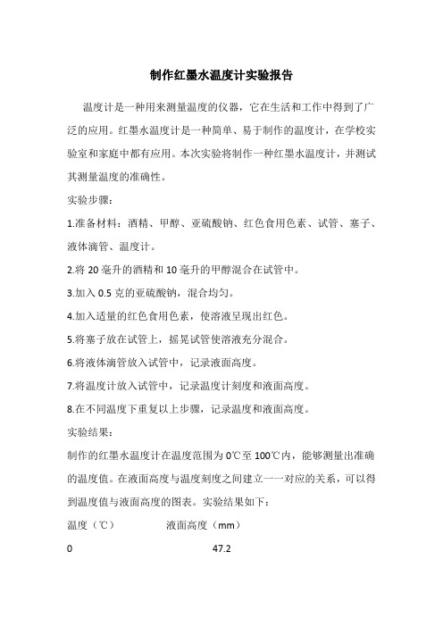
制作红墨水温度计实验报告温度计是一种用来测量温度的仪器,它在生活和工作中得到了广泛的应用。
红墨水温度计是一种简单、易于制作的温度计,在学校实验室和家庭中都有应用。
本次实验将制作一种红墨水温度计,并测试其测量温度的准确性。
实验步骤:1.准备材料:酒精、甲醇、亚硫酸钠、红色食用色素、试管、塞子、液体滴管、温度计。
2.将20毫升的酒精和10毫升的甲醇混合在试管中。
3.加入0.5克的亚硫酸钠,混合均匀。
4.加入适量的红色食用色素,使溶液呈现出红色。
5.将塞子放在试管上,摇晃试管使溶液充分混合。
6.将液体滴管放入试管中,记录液面高度。
7.将温度计放入试管中,记录温度计刻度和液面高度。
8.在不同温度下重复以上步骤,记录温度和液面高度。
实验结果:制作的红墨水温度计在温度范围为0℃至100℃内,能够测量出准确的温度值。
在液面高度与温度刻度之间建立一一对应的关系,可以得到温度值与液面高度的图表。
实验结果如下:温度(℃)液面高度(mm)0 47.210 44.520 41.830 39.040 36.250 33.560 30.870 28.180 25.490 22.6100 19.9实验结论:本次实验制作的红墨水温度计能够准确测量温度,并与常规温度计的测量结果相符。
通过实验数据的图表可知,温度与液面高度之间呈现线性关系,即液面高度随温度的升高而下降。
因此,我们可以用红墨水温度计来测量温度,达到简单、易制作、成本低廉的目的。
总之,本次实验成功制作了红墨水温度计,并测试了它的测量准确性。
红墨水温度计的制作和使用简单便捷,具有一定的实用性,可以在学校实验室和家庭中得到广泛应用。
BGA 红墨水实验

10
将 零 件 放 在 显 微 镜 下 观 察 ,并 判 断 是 从 何 处 断裂。(如附件一)
依断裂处分成四种
Type。
11
再判断红墨水渗透比例为多少% 二)
。(如附件 依 5% 、7 5~ 100% 五 个 等 级 。
-------------------------------------------------------------------------附--件--二 : 红色染剂渗透面积
BGA 零件四周都需滴红墨水。
7
将板子放入烘箱内烘烤,使红墨水干燥。
烘箱条件 : 120℃ ,20 分钟。 (如图四)
8
趁热将板子用力扭曲,使零件尽量与 板分离。
PCB 1.注意不要将板子折断。 2.板子会烫手,记得戴棉质手套。
9
趁热再利用小支一字起子将零件扳开。 (如图五)
1.注意力道不可将零件扳坏掉,如 果还是扳不开可以再继续烘烤数分 钟。 2.板子会烫手,记得戴棉质手套。
12 将结果制作成报告。(参考附件模板)
红墨水(Dye&Pry) 操 作 标 准
图 (一) 图 (二)
图 (三)
红墨水(Dye&Pry) 操 作 标 准
图 (四) 图 (五)
红墨水(Dye&Pry) 操 作 标 准
附件一 :零件断裂 处
Separation Mode Summary
T-1 Type 1 – Substrate T-2 cTryapteer2 – Ball to T-3 sTuybpset3ra–teBall to board T-4 Type 4 – Board crater
10将零件放在显微镜下观察并判断是从何处依断裂处分成四种type11再判断红墨水渗透比例为多少
红墨水染色法

红墨水染色法
红墨水染色法是一种将物质中的某种成分用墨水溶液染色的方法。
红墨水通常是红色的,可以从市场上购买到。
这种染色法常用于实验室中的化学分析和生物学实验中。
红墨水染色法的步骤通常包括以下几个步骤:
1. 准备样品:将待染色的物质样品准备好,可以是固体、液体或气体。
2. 制备红墨水溶液:将红墨水溶解在适量的溶剂中,例如水或乙醇。
3. 添加红墨水溶液:将红墨水溶液逐渐加入到样品中,直到达到所需的染色程度。
4. 混合均匀:轻轻搅拌或摇动样品,使红墨水溶液和样品充分混合。
5. 观察结果:观察样品的变化,例如物质的颜色是否发生变化或产生可见的反应。
红墨水染色法的优点包括操作简便、成本低廉和染色效果明显。
然而,需要注意的是红墨水染色法不能用于所有类型的物质,某些物质可能与红墨水产生反应,导致不准确的结果。
因此,在使用红墨水染色法时应根据具体情况进行正确的选择和操作。
雷诺实验的实验原理和方法

5实验二雷诺实验一、实验目的1、观察流体在管内流动的两种不同流动型态。
2、测定临界雷诺数R ec 。
二、实验原理流体流动有两种不同型态,即层流(或称滞流)和紊流(或称湍流),这一现象最早是由雷诺(Reynolds )于1883年首先发现的。
流体作层流流动时,其流体质点作平行于管轴的直线运动,且在径向无脉动;流体作紊流流动时,其流体质点除沿管轴方向作向前运动外,还在径向作脉动,从而在宏观上显示出紊乱地向各个方向作不规则的运动。
流体流动型态可用雷诺数(Re )来判断,这是一个由各影响变量组合而成的无因次数群,故其值不会因采用不同的单位制而不同。
但应当注意,数群中各物理量必须采用同一单位制。
若流体在圆管内流动,则雷诺数可用下式表示:μνρd =Re (16-1)式中:Re —雷诺数,无因次;d —管子内径,m ;v —流体在管内的平均流速,m /s ;ρ—流体密度,kg /m 3;μ—流体的动力粘滞系数;Pa·s 。
层流转变为紊流时的雷诺数称为临界雷诺数,用R ek 表示。
工程上一般认为,流体在直圆管内流动时,当Re <2000时为层流;当Re >4000时,圆管内已形成紊流;当Re 在2000至4000范围内,流动处于一种过渡状态,可能是层流,也可能是紊流,或者是二者交替出现,这要视外界干扰而定,一般称这一Re 数范围为过渡区。
式(1)表明,对于一定温度的流体,在特定的圆管内流动,雷诺数仅与流体流速有关。
本实验即是通过改变流体在管内的速度,观察在不同雷诺数下流体的流动型态。
三、实验装置与设备参数装置主要由玻璃试验导管、流量计、流量调节阀、低位贮水槽、循环水泵、稳压溢流水槽等部分组成,演示主管路为220⨯φmm 硬质玻璃。
实验装置如图16-1所示:四、实验方法:实验前,先将水充满低位贮水槽,关闭流量计后的调节阀,然后启动循环水泵。
待水充满稳压溢流水槽后,开启流量计后的调节阀。
水由稳压溢流水槽流经缓冲槽、试验导管和流量计,最后流回低位贮水槽。
染色实验(红墨水实验)流程
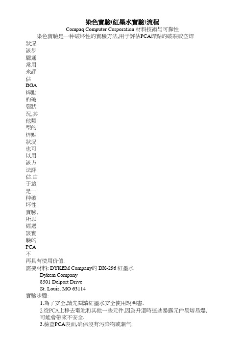
狀況.該步驟通常用來評估BGA 焊點的破裂狀況,其他類型的焊點狀況也可以用該方法評估.由于這是一种破坏性實驗,所以經過該實驗的PCA 不所以這一步一定要戴口罩和保護手套.水沒有被烘干,那么它可能會沾污一個好的焊點的斷面.需要材料: DYKEM Company 的 DX-296 紅墨水Dykem Company8501 Delport Drive1.為了安全,請先閱讀紅墨水安全使用說明書.2.從PCA上移去電池和其他一些元件,因為升溫時這些暴露元件易熔易爆,實驗步驟:3.檢查PCA 表面,确保沒有污染物或潮气.4.用擠壓瓶將清洗劑(異丙醇)噴到BGA底部,驅散清洗劑并用空气壓縮机吹干.重复該動作兩三次,保證PCA 板在染色前完全干燥.5.可通過下列四种方式染色:浸泡,涂刷,噴洒和從四邊用滴管滴.確保紅墨染色實驗(紅墨水實驗)流程Compaq Computer Corporation 材料技術与可靠性染色實驗是一种破坏性的實驗方法,用于評估PCA 焊點的破裂或空焊St. Louis, MO 63114再具有使用价值.可能會帶來不安全.水覆蓋所有要檢驗的BGA 下面的焊點領域.由于紅墨水有毒并且易揮發,6.將PCA 板放進烤箱烘烤.烘烤時間可以因溫度不同而變化(例如,120C 需要2 hours,70 C 則需要8 hours),只要將紅墨水徹底烘干就可以了.7.移去BGA.輕微地彎曲PCA 板以弱化結合點,然后用工具輕輕地移去BGA,注意工具不能損傷我們關注的接點表面(在這儿破裂可能發現的最多).8.用紅墨水沾污檢查焊點質量.染色后破裂或空焊的焊點在斷層表面上會展現出紅色沾污.從下面的顯微照片看出這個BGA 焊點部分破裂.9.沒有延伸到圓周外的內部破裂的焊點,不會有沾污.如果BGA移去時紅墨。
红墨水试验

Description of the Method Developed for Dye Penetrant Analysis of Cracked Solder JointsBackgroundThe extension of cracks in solder joints after fatigue testing is usually evaluated using cross-sectioning of the solder joints. The printed board assembly, or a part of it, is potted in epoxy and is then cut close to the solder joints that will be examined and the sample is ground in to the solder joints. As shown in Figure 1, the formation of cracks in solder joints can be very irregular and vary considerably even in joints located close to each other.Figure 1 Photograph showing the extent an irregularity of cracking in solder joints to a BGA after thermal cycling. The cracking has been analysed using a dyepenetrant and the areas coloured red indicate how far the cracks hadpropagated during the thermal test.Thus, to obtain a three-dimensional view of the extension of cracking in a solder joint, polishing must be done in steps while the extension of cracking is successively documented. Just making one cut through a solder joint may give a completing misleading result. For example, if a cut is made from A to B in Figure 1, it would indicate a completely cracked joint whereas a cut from C to D would indicate that almost no cracking has occurred. Furthermore, a number of solder joints need to be examined in order to get statistically valid results. All solder joints in a row can be examined simultaneously. If all solder joints to a BGA shall be examined, this must be repeated for every row of joints. This is a very time consuming and costly process. Furthermore, it is difficult to determine the exact position of a cut.As already shown in Figure 1, dye penetrant analysis offers a three-dimensional view of cracks in solder joints to a component. The technique was originally developed by Motorola’s Land Mobile Products Sector’s Advanced Manufacturing Technology group [1]. The component assembled on the printed circuit board was flooded with a dye penetrant liquid to define the cracked area. After having applied the dye, the component was removed by bending the board numerous times. The fractured solder joints were then visually inspected and photographs were made to record the position that dye had penetrated into the joint. This method works well if the cracks in the solder joints are large. If they are not large enough, the pads on the board will rip off from the laminate.In order to facilitate the removal of components with small cracks in the solder joints, IVF has improved the technique to remove the components in a project funded by ESA [2]. Application of DyeIn order to facilitate the application of the dye, a dam is created around the component using a modelling wax. If there are via holes beneath the component, a tape is applied to the via holes on the opposite side of the board to prevent the dye from escaping through them. If that is not possible, the sample is laid in a glass beaker. The dam is then filled with the dye (Steel Red from DYKEM) or alternatively the dye is poured into the glass beaker until the sample is completely submerged in the dye. The board or the glass beaker is placed in a vacuum chamber and two evacuations are made down to 100 mbar in order to remove any air entrapped in the cracks. Since solvents in the dye evaporate during this process, it is done as fast as possible to prevent the viscosity of the dye getting too high. The surplus dye is then poured out and the sample is dried at 100°C for 15 minutes.Removal of ComponentsThe upper side of the component package is roughened using a grinding paper and is then dried with a cloth wetted with acetone. A steel cylinder with a threaded hole is glued to the component using a two-part epoxy glue, Plastic Padding Super Steel from Loctite (Fig. 2). The steel cylinder is shotblasted in order to improve the adhesion of the glue.The board is then fixed by screws to an aluminium plate with a thickness of 1 cm. A hook is screwed to the steel cylinder and the sample is arranged so that a pulling force can be applied through the hook (Fig. 3). For BGA components having only peripheral joints it may be better to drill a hole through the component and apply a pulling force as shown in Figure 4. The aluminium plate is placed on a heating plate with the heat controlled by a thermocouple attached to the upper side of the board. The temperatures of the solder joints are registered using another thermocouple.A pulling force of about 50 grams per joint is applied to the package. This force causes the solder to creep and the package can be removed without bending the board. If the solder joints are severely cracked, it may be possible to remove the package within a few hours at room temperature. However, in most cases it is necessary to heat the samples to be able to remove the packages within a reasonable time. The higher temperature, the faster is it possible to remove the component. By heating the solder joints to 140°C, even packages with only small cracks in corner joints can be removed within a few hours. However, at temperatures above 120°, the colour of the dye fades slightly. Also, a good temperature control system is required to ensure that the temperature of the board will not rise above the melting point of the solder when the package becomes loose. If the maximum temperature is limited to 120°C, it may take 10-40 hours to remove a BGA component having about 600 I/Os if the cracks are very small in the solder joints.Figure 2. A component with a steel cylinder glued to itFigure 3. Arrangement for applying a pulling force to a packageFigure 1 Arrangement for applying a pulling force to a BGA by drilling a hole through the component.Case Study of DBGAThis example taken from Reference 2 shows how dye penetrant analysis has been used to evaluate the extent of cracking in solder joints to two thermally cycled Dimple BGA (DBGA) packages.Test VehicleThe DBGA packages had a body size of 17 x 17 mm and 228 I/Os with a pitch of 1.0 mm. Both packages had daisy chain interconnections. The packages were soldered to a multilayer polyimide/glass board with tin-lead plated pads using vapour phase soldering. A flux was added to promote wetting but no additional solder. One package was soldered to a footprint with round solder pads (Component A) whereas the second package was soldered to a footprint having pads with a teardrop form (Component CX).The test vehicle had been thermally cycled in air per ESA-PSS-01-738 with temperature extremes of –55 and +125°C. The cycling was stopped after 500 cycles. The package soldered to the footprint with round pads still functioned electrically after the thermal cycling test but one electrical defect had occurred in one row of I/Os on the other package.Dye Penetrant AnalysisThe extent of cracking in the solder joints to the two DBGA packages was analysed using the procedure for dye penetrant analysis described previously. The solder joints were heated to about 100°C during the removal of the components. At this temperature, the components were removed within 30 minutes.All solder balls remained on the printed circuit board for both packages. The fractures in the solder joints were very close to the component pads for all solder joints (Fig. 5). The majority of the solder joints were severely cracked for both components and to about the same extent (Fig. 6). The fractures in some corner solder joints were coloured completely red (Fig. 7). Thus, although failure had only been registered for Component CX, failure for Component A must have been imminent.Figure 5. View of solder balls remaining on the PCB after removal of Component CXFigure 6. Extent of cracking in Component A (a) and to Component CX (b) analysed using dye penetrantFigure 7. Close-up of the fracture to corner joints to Component A (a) and to Component CX (b). NP = Neutral Point.The remaining solder balls on the PCB were broken away at some locations by gripping them with a micro-tweezer and pulling vertically to the board surface. This enabled us to examine the integrity of the joints towards the board pads. In all cases, the pads were ripped off from the laminate. For a connection in the inner row, no fracture in the laminate could be observed(Fig. 8) whereas extensive cracking was observed for corner joints (Fig. 9). The cracks had formed on the inward side of the joints. For one solder joint, the “inside” of the via-in-pad was coloured red indicating damages to the copper plating in the via hole (Fig. 10). The results were similar for Component CX (Figs. 11-13).Figure 8. Views showing the fracture between a pad and the board laminate for a ball in the inner row to Component A. View (a) shows the ball with the underside of theripped-off pad and view (b) shows the location on the PCB where the ball wasattachedFigure 9. Views showing the fracture between a pad and the board laminate for a corner ball to Component A. View (a) shows the ball with the underside of the ripped offpad and view (b) shows the location on the PCB where the ball was attachedFigure 10. Views showing the fracture between a pad and the board laminate for a corner ball to Component A. View (a) shows the ball with the underside of the ripped offpad and view (b) shows the location on the PCB where the ball was attachedFigure 11. Views showing the fracture between a pad and the board laminate for a ball in the inner row to Component CX. View (a) shows the ball with the underside of theripped off pad and view (b) shows the location on the PCB where the ball wasattachedFigure 12. Views showing the fracture between a pad and the board laminate for a corner ball to Component A. View (a) shows the ball with the underside of the ripped offpad and view (b) shows the location on the PCB where the ball was attachedFigure 13. Views showing the fracture between a pad and the board laminate for a corner ball to Component A. View (a) shows the ball with the underside of the ripped offpad and view (b) shows the location on the PCB where the ball was attached.References1 S. C. Bolton, A. J. Mawer, and E. Mammo, Influence of Plastic Ball Grid ArrayDesign/Materials Upon Solder Joint Reliability, The International Journal ofMicrocircuits and Electronic Packaging, Vol. 18, No. 2 , 1995, pp. 109-120.2 P.-E. Tegehall and B. Dunn, Assessment of the Reliability of Solder Joints to Ball andColumn Grid Array Packages for Space Applications, ESA STM-266, ESAPublications Division, Noordwijk, 2001。
花插红墨水蓝墨水瓶变色实验作文

花插红墨水蓝墨水瓶变色实验作文花插红墨水蓝墨水瓶变色实验。
哇,这花真的变色了!我刚才把红墨水倒进去,没想到这么一会儿,花瓣边缘就开始泛红了,好像害羞的小姑娘。
哈哈,我又换了蓝墨水,这回看看会有什么变化。
哎呀,这花好像变得更美了,蓝色让它看起来更加清新脱俗。
咦,等等,红墨水和蓝墨水混合在一起,怎么变成紫色了?这花也太神奇了吧,简直就是个小魔术师!
这次实验真是太好玩了,没想到花和墨水能有这么多的变化。
看来以后我得多试试不同的组合,看看还能玩出什么新花样!。
- 1、下载文档前请自行甄别文档内容的完整性,平台不提供额外的编辑、内容补充、找答案等附加服务。
- 2、"仅部分预览"的文档,不可在线预览部分如存在完整性等问题,可反馈申请退款(可完整预览的文档不适用该条件!)。
- 3、如文档侵犯您的权益,请联系客服反馈,我们会尽快为您处理(人工客服工作时间:9:00-18:30)。
Red Dye Penetration Test(渗透染红试验)
是检验电子零件的表面贴着技术(SMT)有无空焊或是断裂(crack)的一种技术。
这是一种破怀性的实验,通常被运用在电子电路板组装(PCB Assembly)的表面贴着技术(SMT)上,可以帮助工程师们检查电子零件的焊接是否有瑕疵。
因为是破坏性实验,一般仅运用在已经无法经由其它非破坏性方法检查出问题的电路板上面,而且几乎都只运用在分析
BGA(Ball Grid Array) 封装的 IC,通常是为了可以更了解产品的不良现象,以作为后续生产的质量改善参考,或是为了厘清责任时使用。
其方法是利用适当黏稠度的红药水(红墨水)注射到怀疑有焊习性不良的 BGA IC 底下,要先确认红药水已经完全进入到 BGA IC 底下,等一段时间或烘烤待红药水干了以后,用工具(通常是一字起子)从电路板(PCB)上直接撬起,也有用胶黏住 BGA IC 然后用拉拔机器把 IC 硬取下来的。
要注意:加热温度不可操过焊锡重新熔融的温度。
其实我觉得这个方法满像一般水电或管路工人在抓漏的道理,先倒一点有明显颜色的溶剂,然后看看那边渗漏。
以上是自己土法炼钢的方法,较专业的方法应该要把电路板上怀疑有焊接(solder)问题的地方切割下来,然后将其整个浸泡到红药水当中,再放入超音波振荡机(Ultrasonic cleaner)中震荡一段时间,让红药水可以均匀地渗透到所有的裂缝深处,然后再取出烘烤,烘烤目的只是要烘干红药水而已,所以不需要使用太高的温度,然后把待测样品夹到治具中,将 BGA IC 拉开电路板,然后用高倍显微镜观察其染色现象。
观察已经被撬起的电路板焊垫(pads)及IC的焊球(balls)是否有被染红的痕迹,如果有焊接不良,例如裂痕、空焊等现象应该都可以看得出来有红药水的痕迹。
其原理是利用液体具有渗透(penetration)的特性,可以渗透到所有的缝隙来判断焊接是否完好。
一般的 BGA IC,其焊球的两端应该要个别连接到电路板及BGA IC本体,如果在原本应该是焊接的球形地方出现了红色药水,就表示这个地方有空隙,也就是有焊接断裂,再由焊接断裂的粗糙表面来判断是原本的焊接不良,或是后天不当使用后所造成的断裂。
一般来说,空焊及焊接不良的焊锡表面呈现圆滑状,因为焊锡具有较强的内聚力,但也有例外,比如说氧化或异物污染亦会形成粗糙面;至于后天断裂的表面则呈现较不规则的尖锐凹凸表面。
↓下图为 Dye Penetration Test 的结果,可以很明显的看出来左下角有很多颗的 BAG 焊球垫有沾染到红药水,表示这几颗的焊球(balls)有空焊或断裂的情形。