MAX809中文资料_数据手册_参数
MAX809J中文资料

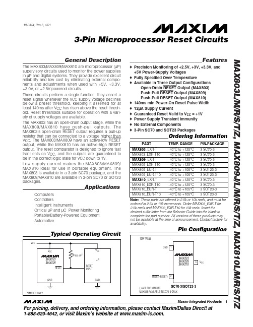
General Description The MAX803/MAX809/MAX810 are microprocessor (µP) supervisory circuits used to monitor the power supplies in µP and digital systems. They provide excellent circuit reliability and low cost by eliminating external compo-nents and adjustments when used with +5V, +3.3V, +3.0V, or +2.5V-powered circuits.These circuits perform a single function: they assert a reset signal whenever the V CC supply voltage declines below a preset threshold, keeping it asserted for at least 140ms after V CC has risen above the reset thresh-old. Reset thresholds suitable for operation with a vari-ety of supply voltages are available.The MAX803 has an open-drain output stage, while the MAX809/MAX810 have push-pull outputs. The MAX803’s open-drain RESET output requires a pull-up resistor that can be connected to a voltage higher than V CC. The MAX803/MAX809 have an active-low RESET output, while the MAX810 has an active-high RESET output. The reset comparator is designed to ignore fast transients on V CC, and the outputs are guaranteed to be in the correct logic state for V CC down to 1V.Low supply current makes the MAX803/MAX809/ MAX810 ideal for use in portable equipment. The MAX803 is available in a 3-pin SC70 package, and the MAX809/MAX810 are available in 3-pin SC70 or SOT23 packages.Applications ComputersControllersIntelligent InstrumentsCritical µP and µC Power MonitoringPortable/Battery-Powered EquipmentAutomotive ____________________________Features o Precision Monitoring of +2.5V, +3V, +3.3V, and +5V Power-Supply Voltageso Fully Specified Over Temperatureo Available in Three Output ConfigurationsOpen-Drain RESET Output (MAX803)Push-Pull RESET Output (MAX809)Push-Pull RESET Output (MAX810)o140ms min Power-On Reset Pulse Widtho12µA Supply Currento Guaranteed Reset Valid to V CC= +1Vo Power Supply Transient Immunityo No External Components o3-Pin SC70 and SOT23 Packages MAX803L/M/R/S/T/Z, MAX809J/L/M/R/S/T/Z, MAX810L/M/R/S/T/Z3-Pin Microprocessor Reset Circuits________________________________________________________________Maxim Integrated Products1Pin Configuration Typical Operating Circuit19-0344; Rev 4; 12/99Note: These parts are offered in 2.5k or 10k reels, and must beordered in 2.5k or 10k increments. Order MAX803_EXR-T for2.5k reels and MAX803_EXR-T10 for 10k reels. Insert thedesired suffix letter from the Selector Guide into the blank tocomplete the part number. All versions of these products maynot be available at the time of announcement. Contact factory foravailability.For free samples & the latest literature: , or phone 1-800-998-8800. For small orders, phone 1-800-835-8769.Ordering InformationM A X 803L /M /R /S /T /Z , M A X 809J /L /M /R /S /T /Z , M A X 810L /M /R /S /T /Z3-Pin Microprocessor Reset CircuitsABSOLUTE MAXIMUM RATINGSELECTRICAL CHARACTERISTICS(V CC = full range, T A = -40°C to +105°C, unless otherwise noted. Typical values are at T A = +25°C, V CC = 5V for L/M/J versions, V CC = 3.3V for T/S versions, V CC = 3V for R version, and V CC = 2.5V for Z version.) (Note 1)Stresses beyond those listed under “Absolute Maximum Ratings” may cause permanent damage to the device. These are stress ratings only, and functional operation of the device at these or any other conditions beyond those indicated in the operational sections of the specifications is not implied. Exposure to absolute maximum rating conditions for extended periods may affect device reliability.Terminal Voltage (with respect to GND)V CC ....................................................................-0.3V to +6.0V RESET, RESET (push-pull).....................-0.3V to (V CC + 0.3V)RESET (open drain)...........................................-0.3V to +6.0V Input Current, V CC ..............................................................20mA Output Current, RESET, RESET ..........................................20mA Rate of Rise, V CC ............................................................100V/µsContinuous Power Dissipation (T A = +70°C)3-Pin SC70 (derate 2.17mW/°C above +70°C)............174mW 3-Pin SOT23 (derate 4mW/°C above +70°C)...............320mW Operating Temperature Range .........................-40°C to +105°C Storage Temperature Range.............................-65°C to +150°C Lead Temperature (soldering, 10s).................................+300°CMAX803L/M/R/S/T/Z, MAX809J/L/M/R/S/T/Z, MAX810L/M/R/S/T/Z3-Pin Microprocessor Reset Circuits_______________________________________________________________________________________3A Note 2:RESET output for MAX803/MAX809; RESET output for MAX810.POWER-DOWN RESET DELAY vs. TEMPERATURE (MAX8_ _R/S/T/Z)80100TEMPERATURE (°C)P O W E R -D O W N R E S E T D E L A Y (µs )402060-408520-2006040Typical Operating Characteristics(V CC = full range, T A = -40°C to +105°C, unless otherwise noted. Typical values are at T A = +25°C, V CC = +5V for L/M/J versions,V CC = +3.3V for T/S versions, V CC = +3V for R version, and V CC = +2.5V for Z version.)ELECTRICAL CHARACTERISTICS (continued)(V CC = full range, T A = -40°C to +105°C, unless otherwise noted. Typical values are at T A = +25°C, V CC = 5V for L/M/J versions, V CC = 3.3V for T/S versions, V CC = 3V for R version, and V CC = 2.5V for Z version.) (Note 1)-402040-206085SUPPLY CURRENT vs. TEMPERATURE(SC70 PACKAGE, NO LOAD)TEMPERATURE (°C)S U P P L Y C U R R E N T (µA )051015M A X 803L /M /R /S /T /Z , M A X 809J /L /M /R /S /T /Z , M A X 810L /M /R /S /T /Z3-Pin Microprocessor Reset Circuits 4_______________________________________________________________________________________Typical Operating Characteristics (continued)(V CC = full range, T A = -40°C to +105°C, unless otherwise noted. Typical values are at T A = +25°C, V CC = +5V for L/M/J versions,V CC = +3.3V for T/S versions, V CC = +3V for R version, and V CC = +2.5V for Z version.)225POWER-UP RESET TIMEOUTvs. TEMPERATURE245250TEMPERATURE (°C)P O W E R -U P R E S E T T I M E O U T (m s )235230240-408520-2060400.997NORMALIZED RESET THRESHOLDvs. TEMPERATURE1.0011.0021.003M A X 803-T O C 6TEMPERATURE (°C)N O R M A L I Z E D T H R E S H O L D0.9990.9981.000-408520-206040Selector Guide0POWER-DOWN RESET DELAY vs. TEMPERATURE (MAX8_ _J/L/M)80100120140TEMPERATURE (°C)P O W E R -D O W N R E S E T D E L A Y (µs )402060-408520-2006040MAX803L/M/R/S/T/Z, MAX809J/L/M/R/S/T/Z, MAX810L/M/R/S/T/Z_______________________________________________________________________________________5Detailed DescriptionA microprocessor’s (µP’s) reset input starts the µP in a known state. The MAX803/MAX809/MAX810 assert reset to prevent code-execution errors during power-up, power-down, or brownout conditions. They assert a reset signal whenever the V CC supply voltage declines below a preset threshold, keeping it asserted for at least 140ms after V CC has risen above the reset thresh-old. The MAX803 uses an open-drain output, and the MAX809/MAX810 have a push-pull output stage.Connect a pull-up resistor on the MAX803’s RESET out-put to any supply between 0 and 6V.Applications InformationNegative-Going V CC TransientsIn addition to issuing a reset to the µP during power-up,power-down, and brownout conditions, the MAX803/MAX809/MAX810 are relatively immune to short-duration negative-going V CC transients (glitches).Figure 1 shows typical transient duration vs. reset com-parator overdrive, for which the MAX803/MAX809/MAX810 do not generate a reset pulse. The graph was generated using a negative-going pulse applied to V CC ,starting 0.5V above the actual reset threshold and end-ing below it by the magnitude indicated (reset compara-tor overdrive). The graph indicates the maximum pulse width a negative-going V CC transient can have without causing a reset pulse. As the magnitude of the transient increases (goes farther below the reset threshold), the maximum allowable pulse width decreases. Typically, for the MAX8__L and MAX8__M, a V CC transient that goes 100mV below the reset threshold and lasts 20µs or less will not cause a reset pulse. A 0.1µF bypass capacitor mounted as close as possible to the V CC pin provides additional transient immunity.Ensuring a Valid Reset OutputDown to V CC = 0When V CC falls below 1V, the MAX809 RESET output no longer sinks current—it becomes an open circuit.Therefore, high-impedance CMOS logic inputs con-nected to RESET can drift to undetermined voltages.This presents no problem in most applications since most µP and other circuitry is inoperative with V CC below 1V. However, in applications where RESET must be valid down to 0V, adding a pull-down resistor to RESET causes any stray leakage currents to flow to3-Pin Microprocessor Reset CircuitsFigure 2. RESET Valid to V CC = Ground Circuit_____________________Pin DescriptionFigure 1. Maximum Transient Duration Without Causing a Reset Pulse vs. Reset Comparator OverdriveM A X 803L /M /R /S /T /Z , M A X 809J /L /M /R /S /T /Z , M A X 810L /M /R /S /T /Zground, holding RESET low (Figure 2). R1’s value is not critical; 100k Ωis large enough not to load RESET and small enough to pull RESET to ground.A 100k Ωpull-up resistor to V CC is also recommended for the MAX810 if RESET is required to remain valid for V CC < 1V.Interfacing to µPs with Bidirectional Reset PinsSince the RESET output on the MAX803 is open drain,this device interfaces easily with µPs that have bidirec-tional reset pins, such as the Motorola 68HC11.Connecting the µP supervisor’s RESET output directly to the microcontroller’s (µC’s) RESET pin with a single pull-up resistor allows either device to assert reset (Figure 3).MAX803 Open-Drain RESET Output Allows Use with Multiple SuppliesG enerally, the pull-up connected to the MAX803 will connect to the supply voltage that is being monitored at the IC’s V CC pin. However, some systems may use the open-drain output to level-shift from the monitored sup-ply to reset circuitry powered by some other supply (Figure 4). Note that as the MAX803’s V CC decreases below 1V, so does the IC’s ability to sink current at RESET . Also, with any pull-up, RESET will be pulled high as V CC decays toward 0. The voltage where this occurs depends on the pull-up resistor value and the voltage to which it is connected.Benefits of Highly AccurateReset ThresholdMost µP supervisor ICs have reset threshold voltages between 5% and 10% below the value of nominal sup-ply voltages. This ensures a reset will not occur within 5% of the nominal supply, but will occur when the sup-ply is 10% below nominal.When using ICs rated at only the nominal supply ±5%,this leaves a zone of uncertainty where the supply is between 5% and 10% low, and where the reset may or may not be asserted.The MAX8__L/T/Z use highly accurate circuitry to ensure that reset is asserted close to the 5% limit, and long before the supply has declined to 10% below nominal.3-Pin Microprocessor Reset Circuits 6_______________________________________________________________________________________Figure 4. MAX803 Open-Drain RESET Output Allows Use with Multiple SuppliesFigure 3. Interfacing to µPs with Bidirectional Reset I/OTRANSISTOR COUNT:275 (SOT23)380 (SC70)___________________Chip InformationMAX803L/M/R/S/T/Z, MAX809J/L/M/R/S/T/Z, MAX810L/M/R/S/T/Z3-Pin Microprocessor Reset Circuits_______________________________________________________________________________________7Package InformationM A X 803L /M /R /S /T /Z , M A X 809J /L /M /R /S /T /Z , M A X 810L /M /R /S /T /Z3-Pin Microprocessor Reset Circuits Maxim cannot assume responsibility for use of any circuitry other than circuitry entirely embodied in a Maxim product. No circuit patent licenses are implied. Maxim reserves the right to change the circuitry and specifications without notice at any time.8_____________________Maxim Integrated Products, 120 San Gabriel Drive, Sunnyvale, CA 94086 408-737-7600©1999 Maxim Integrated ProductsPrinted USAis a registered trademark of Maxim Integrated Products.Package Information (continued)。
MAX809RTRG中文资料
Supply Voltage (Typ)
ABSOLUTE MAXIMUM RATINGS
Rating
Symbol
Value
Unit
Power Supply Voltage (VCC to GND) RESET rrent, VCC Output Current, RESET
VCC
The MAX809/810 are optimized to reject fast transient glitches on the VCC line. Low supply current of 0.5 mA (VCC = 3.2 V) makes these devices suitable for battery powered applications.
MAX809 Series, MAX810 Series
ELECTRICAL CHARACTERISTICS TA = −40°C to +105°C unless otherwise noted. Typical values are at TA = +25°C. (Note 3)
Characteristic
Typical Applications
• Computers • Embedded Systems • Battery Powered Equipment • Critical Microprocessor Power Supply Monitoring
MAX809S中文资料
19-0344; Rev 5; 1/01
3-Pin Microprocessor Reset Circuits
General Description
The MAX803/MAX809/MAX810 are microprocessor (µP) supervisory circuits used to monitor the power supplies in µP and digital systems. They provide excellent circuit reliability and low cost by eliminating external components and adjustments when used with +5V, +3.3V, +3.0V, or +2.5V powered circuits. These circuits perform a single function: they assert a reset signal whenever the VCC supply voltage declines below a preset threshold, keeping it asserted for at least 140ms after VCC has risen above the reset threshold. Reset thresholds suitable for operation with a variety of supply voltages are available. The MAX803 has an open-drain output stage, while the MAX809/MAX810 have push-pull outputs. The MAX803’s open-drain RESET output requires a pull-up resistor that can be connected to a voltage higher than VCC. The MAX803/MAX809 have an active-low RESET output, while the MAX810 has an active-high RESET output. The reset comparator is designed to ignore fast transients on VCC, and the outputs are guaranteed to be in the correct logic state for VCC down to 1V. Low supply current makes the MAX803/MAX809/ MAX810 ideal for use in portable equipment. The MAX803 is available in a 3-pin SC70 package, and the MAX809/MAX810 are available in 3-pin SC70 or SOT23 packages.
MAX809
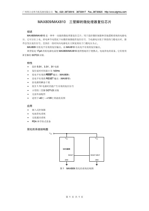
图 3 MAX809 的管脚配置
图 4 MAX810 的管脚配置 第2页共2页
广州周立功单片机发展有限公司 Tel 020 38730916 38730917 Fax 38730925
MAX809 的管脚说明
管脚
符号
1
GND
2
RESET
3
VCC
描述 器件的地 低电平有效复位信号 电源电压输入
广州周立功单片机发展有限公司 Tel 020 38730916 38730917 Fax 38730925
MAX809/MAX810 三管脚的微处理器复位芯片
综述
MAX809/MAX810 是一种单一功能的微处理器复位芯片 用于监控微控制器和其他逻辑系统的电源电 压 它可以在上电 掉电和节电情况下向微控制器提供复位信号 当电源电压低于预设的门槛电压时 器 件会发出复位信号 直到在一段时间内电源电压又恢复到高于门槛电压为止
VCC
VCC
RESET
MAX809
4.7 k Ω
GND
VCC RESET
MOTOROLA 68HCxx GND
图 7 通过双向复位 I/O 接口到微控制器
封装方式
MAX809 和 MAX810 都以卷盘封装 如图 8 所示
第6页共6页
广州周立功单片机发展有限公司 Tel 020 38730916 38730917 Fax 38730925
条件
最小值 -0.3 -0.3
-0.3 -40 -65 在 Tamb=70 以上 时下降 4mW/
最大值 6.0 VCC+0.3
单位 V V
VCC+0.3 20 20 100 +105 +150 320
MAX809SD中文资料
COVER TAPECARRIER TAPEREELAS-SEMBLY TAPE GUARBAND CODELABELBOXFigure 8. Tape and reel packing method.MAX809/MAX810 3-pin microprocessor resetsSOT23-3: plastic small outline package; 3 leads; body width 1.5 mm1.351.21.00.250.500.250.220.083.002.701.701.500.550.352310.150.0510°0°MAX809/MAX810 3-pin microprocessor resetsSC70-3:plastic small outline package; 3 leads; body width 1.15 mm1.0 0.80.40.250.2250.102.11.90.40.1MAX809/MAX810 3-pin microprocessor resetsDefinitionsShort-form specification — The data in a short-form specification is extracted from a full data sheet with the same type number and title. For detailed information see the relevant data sheet or data handbook.Limiting values definition — Limiting values given are in accordance with the Absolute Maximum Rating System (IEC 60134). Stress above one or more of the limiting values may cause permanent damage to the device. These are stress ratings only and operation of the device at these or at any other conditions above those given in the Characteristics sections of the specification is not implied. Exposure to limiting values for extended periods may affect device reliability.Application information — Applications that are described herein for any of these products are for illustrative purposes only. Philips Semiconductors make no representation or warranty that such applications will be suitable for the specified use without further testing or modification.DisclaimersLife support — These products are not designed for use in life support appliances, devices, or systems where malfunction of these products can reasonably be expected to result in personal injury. Philips Semiconductors customers using or selling these products for use in such applications do so at their own risk and agree to fully indemnify Philips Semiconductors for any damages resulting from such application.Right to make changes — Philips Semiconductors reserves the right to make changes in the products—including circuits, standard cells, and/or software—described or contained herein in order to improve design and/or performance. When the product is in full production (status ‘Production’), relevant changes will be communicated via a Customer Product/Process Change Notification (CPCN). Philips Semiconductors assumes no responsibility or liability for the use of any of these products, conveys no license or title under any patent, copyright, or mask work right to these products, and makes no representations or warranties that these products are free from patent, copyright, or mask work right infringement, unless otherwise specified.Contact informationFor additional information please visit.Fax: +31 40 27 24825For sales offices addresses send e-mail to:© Koninklijke Philips Electronics N.V. 2003All rights reserved. Printed in U.S.A.Date of release: 08-03Document order number:9397 750 11889。
MAX809中文资料

ON Semiconductor and are trademarks of Semiconductor Components Industries, LLC (SCILLC). SCILLC reserves the right to make changes without further notice to any products herein. SCILLC makes no warranty, representation or guarantee regarding the suitability of its products for any particular purpose, nor does SCILLC assume any liability arising out of the application or use of any product or circuit, and specifically disclaims any and all liability, including without limitation special, consequential or incidental damages. “Typical” parameters which may be provided in SCILLC data sheets and/or specifications can and do vary in different applications and actual performance may vary over time. All operating parameters, including “Typicals” must be validated for each customer application by customer’s technical experts. SCILLC does not convey any license under its patent rights nor the rights of others.SCILLC products are not designed, intended, or authorized for use as components in systems intended for surgical implant into the body, or other applications intended to support or sustain life, or for any other application in which the failure of the SCILLC product could create a situation where personal injury or death may occur. Should Buyer purchase or use SCILLC products for any such unintended or unauthorized application, Buyer shall indemnify and hold SCILLC and its officers, employees, subsidiaries, affiliates, and distributors harmless against all claims, costs, damages, and expenses, and reasonable attorney fees arising out of, directly or indirectly, any claim of personal injury or death associated with such unintended or unauthorized use, even if such claim alleges that SCILLC was negligent regarding the design or manufacture of the part. SCILLC is an Equal Opportunity/Affirmative Action Employer. PUBLICATION ORDERING INFORMATIONCENTRAL/SOUTH AMERICA:Spanish Phone:303–308–7143 (Mon–Fri 8:00am to 5:00pm MST)Email:ONlit–spanish@ASIA/PACIFIC: LDC for ON Semiconductor – Asia SupportPhone:303–675–2121 (Tue–Fri 9:00am to 1:00pm, Hong Kong Time)Toll Free from Hong Kong & Singapore:001–800–4422–3781Email: ONlit–asia@JAPAN: ON Semiconductor, Japan Customer Focus Center4–32–1 Nishi–Gotanda, Shinagawa–ku, Tokyo, Japan 141–8549Phone: 81–3–5740–2745Email: r14525@。
MAX908中文资料
元器件交易网ห้องสมุดไป่ตู้
MAX907/MAX908/MAX909
Single/Dual/Quad High-Speed, Ultra Low-Power, Single-Supply TTL Comparators
ABSOLUTE MAXIMUM RATINGS
Positive Supply Voltage (V+ to GND) . . . . . . . . . . . . . . . . . . . . . . . . +7V Negative Supply Voltage (V- to GND, MAX909 only) . . . . . . . . . -7V Differential Input Voltage
High-Speed Sampling Circuits
Zero Crossing Detectors
___________________________Features
o 40ns Propagation Delay o 700µA (3.5mW) Supply Current per Comparator o Single 4.5V to 5.5V Supply Operation
________________________________________________________________ Maxim Integrated Products 1
Call toll free 1-800-998-8800 for free samples or literature.
8 CERDIP
Ordering Information continued on last page. * Dice are specified at +25°C, DC parameters only.
MAX809替代料
MAX809替代料Maxim Semiconductor MAX809芯片可采用TOREX XC61F替换XC61F品牌:TOREX产地:日本特点:内置延迟电路的电压检测器代理商:深圳市泰德兰电子有限公司TOREX XC61F系列为内置延迟电路的电压检测器。
采用CMOS工艺和激光微调技术,实现了高精度,低电流消耗。
检测电压精度高,且温度漂移极小。
输出电路有N沟开漏和CMOS 2种。
因内置延迟电路,所以不需要外置元件,可实现高密度安装。
TOREX XC61F可与Maxim Semiconductor MAX809相媲美,替换MAX809芯片TOREX XC61F检测电压范围能够在1.6V~6.0V范围内以0.1V间隔设定;MAX809检测电压+2.5 V,+3 V,+3.3 V和+5 VTOREX XC61F輸出形式N沟道开漏/CMOS輸出;MAX809輸出形式Push-Pull active-low RESET Output (MAX809)TOREX XC61F内置延迟电路1ms~50ms 50ms~200ms 80ms~400msXC61F特征:高电压检测精度±2%低消耗电流1.0μA(TYP.)[VIN=2.0V]检测电压范围能够在1.6V~6.0V范围内以0.1V间隔设定工作电压范围0.7V~10.0V检测电压温度特性±100ppm/℃(TYP.)内置延迟电路1ms~50ms50ms~200ms80ms~400ms輸出形式N沟道开漏/CMOS輸出小型封装SOT-23, SOT-89, TO-92Highly Accurate : ± 2%Low Power Consumption : 1.0μA(TYP.)[ VIN=2.0V ]Detect V oltage Range : 1.6V ~ 6.0V in 0.1V incrementsOperating V oltage Range : 0.7V ~ 10.0VDetect V oltage Temperature Characteristics:±100ppm/℃(TYP.)Built-In Delay Circuit : ①1ms ~ 50ms②50ms ~ 200ms③80ms ~ 400msOutput Configuration : N-ch open drain output or CMOS Packages : SOT-23: SOT-89: TO-92Environmentally Friendly : EU RoHS Compliant, Pb Free XC61F电路图:XC61F引脚配置:TOREX品牌优势:TOREX以提高客户满足度为目标,Torex取得质量管理系统的国际规格ISO9001本公司所提供之产品,由合作工厂生产。
MSP430复位电路(MAX809)
MSP43O单片机复位电路可靠性设计引言TI公司的混合信号处理器MSP430系列单片机以其处理能力强大、外围器件集成度高、功率消耗低、产品系列全面、全系列工业级等特点,作为目前MCU主流市场的产品之一,在电子应用领域中得到广泛应用,被越来越多的电子设计师所青睐。
由于复位电路设计问题而导致的系统出现上电后不工作或状态不正确是很多MSP430单片机电路设计者们在设计、调试和应用中曾遇到过的问题,尽管这种情况发生的几率很低,但对于可靠性要求较高的应用场合,这个现象仍需引起电子设计人员的足够重视。
为此,本文对MSP430全系列单片机的复位系统和复位机制进行了详细深入的分析,并针对性地提出了具体的外围复位电路设计方案和有关电子元器件的详细介绍,以供同行参考和交流。
1、MSP430复位机制1.1 MSP430复位电路MSP430的复位电路包括一个上电复位(POR)和上电清除信号(PUC)。
POR是设备复位信号,它通常在以下三种事件发生时被触发:a.上电;b.复位模式下RST/NMI脚出现低电平;c.电压监控设备(Brownout)触发。
POR时序见图1(a)所示。
当供电电压VCC缓慢上升时,POR监测器保持POR信号有效直到VCC超出VPOR水平;当供电电压VCC快速上升时,POR延时t(POR DELAY)提供了足够长的有效POR信号以确保MSP430有足够的时间进行初始化。
1.2 Brownout电路Brownout电路是电压不足重置功能电路。
它取代了POR检测和POR延时电路。
Brownout电路能够检测到上电或掉电过程中的较低的供电电压值,并能在供电或掉电过程中通过触发POR信号重置芯片。
图l(b)为Brownout电路的复位时序。
从图中看出,当VCC超过启动电压VCC(star-t)时POR 信号有效,POR信号保持有效直到VCC电压值高于极限电压V(B_IT+)并经过一段时间的延时t(BOR);滞后电压Vhys(B_IT-)用于确保供电电压必须低于V(B_IT-)时Brownout电路才会产生下一个POR信号。
MAX809STRG中文资料
(1 ms, 20 ms, 100 ms, and 140 ms)
• RESET Output Guaranteed to VCC = 1.0 V. • Low Supply Current • Compatible with Hot Plug Applications • VCC Transient Immunity • No External Components • Wide Operating Temperature: −40°C to 105°C • Pb−Free Packages are Available
characterization.
2. The maximum package power dissipation limit must not be exceeded.
PD
+
TJ(max) * RqJA
TA
with TJ(max) = 150°C
2
元器件交易网
4.78
−
5.02
4.66
−
5.14
MAX8xxLTR, MAX8xxSQ463 TA = +25°C TA = −40°C to +85°C TA = +85°C to +105°C
4.56
4.63
4.70
4.50
−
4.75
4.40
−
4.86
MAX809HTR TA = +25°C TA = −40°C to +85°C TA = +85°C to +105°C
- 1、下载文档前请自行甄别文档内容的完整性,平台不提供额外的编辑、内容补充、找答案等附加服务。
- 2、"仅部分预览"的文档,不可在线预览部分如存在完整性等问题,可反馈申请退款(可完整预览的文档不适用该条件!)。
- 3、如文档侵犯您的权益,请联系客服反馈,我们会尽快为您处理(人工客服工作时间:9:00-18:30)。
MAX809R/S/T/Z VCC < 3.6 V; MAX810R/S/T/Z Tamb = –40 °C to +85 °C
MAX809J/L/M MAX810J/L/M
VCC < 5.5 V; Tamb = +85 °C to +105 °C
MAX809R/S/T/Z VCC < 3.6 V; MAX810R/S/T/Z Tamb = +85 °C to +105 °C
2003 Aug 08
4
Philips Semiconductors
3-pin microprocessor resets
Product data
MAX809/MAX810
ELECTRICAL CHARACTERISTICS
VCC = full range (Tamb = –40 °C to +105 °C) unless otherwise noted; typical values are at Tamb = +25 °C, and VCC = 5 V (J/L/M versions), VCC = 3.3 V (T/S versions), VCC = 3 V (R version), and VCC = 2.5 V (Z version) (Note 1).
TEMPERATURE RANGE
–40 to +105 °C –40 to +105 °C –40 to +105 °C –40 to +105 °C
Part number
MAX809
MAX809ZD, MAX809ZW
MAX809RD, MAX809RW
MAX809SD, MAX809SW
MAX809TD, MAX809TW
Part
Marking
Part
Marking
MAX809
MAX810
MAX809JD
AMUx
MAX810LD
ANTx
MAX809LD
AMVx
MAX810RD
ANUx
MAX809MD
AMWx
MAX810SD
ANVx
MAX809RD, W AMXx
MAX810JD
ANWx
MAX809SD
AMYx
MAX810MD
• Power supply transient immunity • Guaranteed reset valid for 1.1 V • Available in small SOT23 and SC70 3-pin packages • No external components needed • Specified over full temperature range –40 °C to +105 °C
ICC
Supply current (SC70-3)
MAX809J/L/M VCC < 5.5 V;
MAX810J/L/M Tamb = –40 °C to +85 °C
MAX809R/S/T/Z VCC < 3.6 V; MAX810R/S/T/Z Tamb = –40 °C to +85 °C
MAX809J/L/M MAX810J/L/M
CONDITIONS Derate 4 mW/°C above Tamb = 70 °C
MIN. –0.3 –0.3 –0.3
– – – –40 –65 –
MAX. 6.0
VCC + 0.3 VCC + 0.3
20 20 100 +105 +150 320
UNIT V V V mA mA
V/µs °C °C mW
VCC
VCC
VCC
VCC
VCC
VCC
MAX809
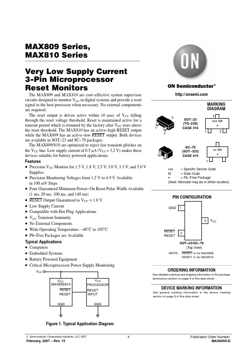
RESET GND
MICROPROCESSOR RESET INPUT
GND
SL01642
Figure 1. MAX809 simplified system diagram.
MAX810
RESET GND
MICROPROCESSOR RESET INPUT
MAX809 3 VCC
RESET 2
SL01641
Figure 3. MAX809 pin configuration.
MAX809 pin description
PIN SYMBOL
DESCRIPTION
1 GND
Device ground.
2 RESET Active-LOW reset signal.
INTEGRATED CIRCUITS
MAX809/MAX810 3-pin microprocessor resets
Product data Supersedes data of 2002 Oct 21
2003 Aug 08
Philips Semiconductors
Philips Semiconductors
MAX809xW
SC70-3
plastic small outline package; 3 leads; body width 1.15 mm
MAX810xW
SC70-3
plastic small outline package; 3 leads; body width 1.15 mm
NOTE: Each device has 7 voltage options, indicated by the ‘x’ on the ‘Type number’.
2 RESET Active-HIGH reset signal.
3 VCC
Supply voltage input.
MAXIMUM RATINGS
SYMBOL
PARAMETER
VCC Vi(RESET) Vi(RESET) Ii(VCC) Io
Tamb Tstg P
Supply voltage Input voltage at RESET pin (MAX809) Input voltage at RESET pin (MAX810) Input current at VCC pin Output current Rate of rise at VCC Ambient temperature Storage temperature Power dissipation
MAX810ZD, MAX810ZW
MAX810RD, MAX810RW
MAX810SD, MAX810SW
MAX810TD, MAX810TW
MAX810JD, MAX810JW
MAX810MD, MAX810MW
MAX810LD, MAX810LW
Reset Threshold Voltage (Typical)
3-pin microprocessor resets
Product data
MAX809/MAX810
DESCRIPTION
The MAX809/MAX810 are single function microprocessor resets used to monitor supply voltages in microprocessor and other logic systems. They provide a reset signal to the microprocessor during power-up, power-down, and brownout conditions. The reset signal is asserted when the supply voltage drops below the preset threshold, and the signal is released a set time after the supply voltage has risen above the preset threshold.
FEATURES
• Monitors 5.0 V, 3.3 V and 3 V supplies • 140 ms min. reset delay time:
– Active-LOW RESET output (MAX809) – Active-HIGH RESET output (MAX810)
APPLICATIONS
• Embedded controllers • Battery operated systems • Wireless communication systems • PDAs and handheld equipment
SIMPLIFIED SYSTEM DIAGRAMS
2.32 V 2.63 V 2.93 V 3.08 V 4.00 V 4.38 V 4.63 V
Marking code
Each device is marked with a four letter code. The first three letters designate the product. The fourth, represented by an ‘x’, designates the date tracking code.
SYMBOL
PARAMETER
CONDITIONS
MIN.
TYP. MAX. UNIT
VCC range
Tamb = 0 °C to +70 °C
Tamb = –40 °C to +105 °C
ICC
Supply current (SOT23-3)
MAX809J/L/M VCC < 5.5 V;