RT8543富佳维
FOSAN富信电子 三极管 2SC945-产品规格书

安徽富信半导体科技有限公司ANHUI FOSAN SEMICONDUCTOR TECHNOLOGY CO.,LTD.2SC945TO-92Bipolar Transistor双极型三极管▉Features特点NPN General Purpose通用▉Absolute Maximum Ratings最大额定值Characteristic特性参数Symbol符号Rat额定值Unit单位Collector-Base Voltage集电极基极电压V CBO60V Collector-Emitter Voltage集电极发射极电压V CEO50V Emitter-Base Voltage发射极基极电压V EBO5V Collector Current集电极电流I C150mA Power dissipation耗散功率P C(T a=25℃)400mW Thermal Resistance Junction-Ambient热阻RΘJA313℃/WJunction and Storage TemperatureT J,T stg-55to+150℃结温和储藏温度■Device Rank产品分档Rank档位O Y GR BLH FE Range70-140120-240200-400350-700ANHUI FOSAN SEMICONDUCTOR TECHNOLOGY CO.,LTD.2SC945■ElectricalCharacteristics 电特性(T A =25℃unless otherwise noted 如无特殊说明,温度为25℃)Characteristic 特性参数Symbol 符号Min 最小值Type 典型值Max 最大值Unit 单位Collector-Base Breakdown V oltage 集电极基极击穿电压(I C =100uA ,I E =0)BV CBO60——VCollector-Emitter Breakdown Voltage 集电极发射极击穿电压(I C =1mA ,I B =0)BV CEO 50——VEmitter-Base Breakdown V oltage 发射极基极击穿电压(I E =100uA ,I C =0)BV EBO 5——VCollector-Base Leakage Current 集电极基极漏电流(V CB =60V ,I E =0)I CBO ——100nA Emitter-Base Leakage Current 发射极基极漏电流(V EB =5V ,I C =0)I EBO——100nADC Current Gain 直流电流增益(V CE =6V ,I C =1mA)H FE 70—700Collector-Emitter Saturation Voltage 集电极发射极饱和压降(I C =100mA ,I B =10mA)V CE(sat)——0.3VBase-Emitter Saturation V oltage 基极发射极饱和压降(I C =100mA ,I B =10mA)V BE(sat)——1V Transition Frequency 特征频率(V CE =6V ,I C =10mA)f T200——MH Z Noise Figure 噪声系数(V CE =6V ,I C =0.1mA,f=1KH Z )NF——10dBOutput Capacitance 输出电容(V CB =10V ,I E =0,f=1MH Z )C ob——3pFANHUI FOSAN SEMICONDUCTOR TECHNOLOGY CO.,LTD.2SC945■Typical Characteristic Curve典型特性曲线ANHUI FOSAN SEMICONDUCTOR TECHNOLOGY CO.,LTD.2SC945■Dimension外形封装尺寸。
VSC854xRT 放射性耐受快速 ги格兹以太网物理单端口 PHY说明书

VSC854xRT Radiation-Tolerant Ethernet PHYSingle-Port, Fast, Gigabit Ethernet Copper PHY With MII, RMII, GMII and RGMIIVSC8541RT Key FeaturesSuperior PHY and Interface Technology• Integrated 10/100/1000BASE-T Ethernet copper trans-ceiver (IEEE ® 802.3ab compliant) with the industry’s only non-TDR-based VeriPHY™ cable diagnostics algorithm • Patented line driver with low EMI voltage mode architec-ture and integrated line-side termination resistors • Wake-on-LAN using magic packets• HP Auto-MDIX and manual MDI/MDIX support • MII, RMII, GMII and RGMII for MAC•Jumbo frame support up to 16 Kilobytes with program-mable synchronization FIFOsSynchronous Ethernet and IEEE 1588 Time Stamp Support • Recovered clock output with programmable clock squelch control for G.8261 Synchronous Ethernet applications • 1000 BASE-T ring resiliency feature to switch between master and slave timing without dropping link • Clock output squelch to inhibit clocks during auto-negotiation and no link status• Clause 45 registers to support IEEE 802.3bf•IEEE 1588 Start of Frame (SOF) detection to enhance1588v2 PTP time stamp accuracyFast Link Up/Link Drop Modes• Fast link failure indication (<1 ms typical, programmable down to <10 μs)•Supports 1000BASE-T forced mode for both master and slave end point configurations with constant link self-monitoring and link auto-reset should the link come downBest-In-Class Power Consumption• EcoEthernet v2.0 green energy efficiency with ActiPHY, PerfectReach and IEEE 802.3az energy-efficient Ethernet• Fully optimized power consumption for all link speeds •Clause 45 registers to support energy-efficient EthernetKey Specifications• Compliant with IEEE 802.3 (10BASE-T, 100BASE-TX, and 1000BASE-T) specifications• Supports MII, RMII, GMII and RGMII• Supports 1.5, 1.8, 2.5 and 3.3V CMOS for RGMII versions 1.3 and 2.0 (without HSTL support), GMII/MII and RMII version 1.2• Supports 25 MHz XTAL and 25/50/125 MHz OSC clock sources• Supports programmable output frequencies of 25, 50 or 125 MHz regardless of chosen XTAL or OSC frequencies • Supports a wide array of stand-alone hardware configura -tion options• Supports all five bits of MDIO/MDC addressing possible for managed-mode designs using pull-up/pull-down resistors•Optionally reports if a link partner is requesting in-line Power over Ethernet (PoE and PoE+)The Microchip name and logo and the Microchip logo are registered trademarks of Microchip Technology Incorporated in the U.S.A. and other countries. All other trademarks mentioned herein are property of their respective companies. © 2021, Microchip Technology Incorporated. All Rights Reserved. 7/21 DS00003337BSpace Environment• Full wafer lot traceability• 68-pin hermetic ceramic CQFP package • Space-grade screening and qualification• Total ionizing dose: up to 100 krad (Si), QML and ESCC)• Heavy ions and protons test• Single event latch-up LET > 78 MeV.cm²/mg •SEU full characterization for all functional blockHiRel/New Space Application• Full wafer lot traceability • 68-pin plastic VQFN package• QML-N/AQEC/AEC-Q100 equivalent• Unitary burn-in and temperature cycling (opt.)• Qual pack documentation •Single lot date codeVSC8540RTThe Radiation-Tolerant, Single-Port, Fast Ethernet Copper PHYTargeting space-constrained 10/100BASE-T applications in both ceramic and plastic packages, the VSC8540RT is a radiation-tolerant, single-port, fast Ethernet copper PHY with RGMII/MII/RMII interfaces that withstands the harsh aerospace environments with enhanced radiation performance and high reliability in extreme temperatures and vacuums. With its equivalent feature set, VSC8540RT is the radiation-tolerant Ethernet PHY solution for customers not requiring gigabit capabilities.VSC8541 Evaluation KitProduct Selection GuideTHERMDATHERMDCP0_D0N P0_D0P P0_D1N P0_D1P P0_D2N P0_D2P P0_D3N P0_D3PRCVRD_CLK CLK_SQUELCH_IN FASTLINK_FAILCLKOUTXTAL1/REFCLK XTAL2REFCLK_SEL[1:0]REF_FILT_A REF_REXT_ALED[1:0]。
高输入阻抗运算放大器

CA3130 高输入阻抗运算放大器Intersil[DA TA]CA3140 高输入阻抗运算放大器CD4573 四可编程运算放大器MC14573ICL7650 斩波稳零放大器LF347(NS[DA TA]) 带宽四运算放大器KA347LF351 BI-FET单运算放大器NS[DA TA]LF353 BI-FET双运算放大器NS[DA TA]LF356 BI-FET单运算放大器NS[DA TA]LF357 BI-FET单运算放大器NS[DA TA]LF398 采样保持放大器NS[DATA]LF411 BI-FET单运算放大器NS[DA TA]LF412 BI-FET双运放大器NS[DA TA]LM124 低功耗四运算放大器(军用档) NS[DA TA]/TI[DATA] LM1458 双运算放大器NS[DATA]LM148 四运算放大器NS[DA TA]LM224J 低功耗四运算放大器(工业档) NS[DA TA]/TI[DATA] LM2902 四运算放大器NS[DATA]/TI[DATA]LM2904 双运放大器NS[DATA]/TI[DATA]LM301 运算放大器NS[DATA]LM308 运算放大器NS[DATA]LM308H 运算放大器(金属封装)NS[DA TA]LM318 高速运算放大器NS[DATA]LM324(NS[DA TA]) 四运算放大器HA17324,/LM324N(TI)LM348 四运算放大器NS[DA TA]LM358 NS[DA TA] 通用型双运算放大器HA17358/LM358P(TI) LM380 音频功率放大器NS[DATA]LM386-1 NS[DATA] 音频放大器NJM386D,UTC386LM386-3 音频放大器NS[DA TA]LM386-4 音频放大器NS[DA TA]LM3886 音频大功率放大器NS[DA TA]LM3900 四运算放大器LM725 高精度运算放大器NS[DA TA]LM733 带宽运算放大器LM741 NS[DA TA] 通用型运算放大器HA17741MC34119 小功率音频放大器NE5532 高速低噪声双运算放大器TI[DA TA]NE5534 高速低噪声单运算放大器TI[DA TA]NE592 视频放大器OP07-CP 精密运算放大器TI[DA TA]OP07-DP 精密运算放大器TI[DA TA]TBA820M 小功率音频放大器ST[DA TA]TL061 BI-FET单运算放大器TI[DATA]TL062 BI-FET双运算放大器TI[DATA] TL064 BI-FET四运算放大器TI[DATA] TL072 BI-FET双运算放大器TI[DATA] TL074 BI-FET四运算放大器TI[DATA] TL081 BI-FET单运算放大器TI[DATA] TL082 BI-FET双运算放大器TI[DATA] TL084 BI-FET四运算放大器TI[DATA]。
Festo VUVS-L30-M52-AD-G38-F8-1C1+G 电磁电压控制5 2单位稳定阀说

Valor
5/2 monoestable eléctrico 31 mm 2.300 l/min 0,25 ... 1 MPa 2,5 ... 10 bar Corredera muelle neumático c UL us - Recognized (OL) IP65 con conector tipo zócalo según IEC 60529 9,4 mm Estrangulable blando indistinto con enclavamiento mediante pulsador prepilotado interno no reversible Superposición positiva 0,4 9,9 l/sbar 49 ms 24 ms 100 % 2.000 µs 3.600 µs 24 V DC: 3,3 W +/- 10 % Aire comprimido según ISO 8573-1:2010 [7:4:4] Opción de funcionamiento con lubricación (necesaria en otro modo de funcionamiento)
2 - riesgo de corrosión moderado -10 ... 60 °C Aire comprimido según ISO 8573-1:2010 [7:4:4] -10 ... 60 °C 510 g Esquema de conexiones forma C, según EN 175301-803 según EN 175301-803 Sobre regleta de bornes
Material de la carcasa
Material de la corredera Material de los tornillos
常用芯片(基准源+运放)

常⽤芯⽚(基准源+运放)⼀、基准源1%级:MC1403,LM336,TL4310.1%:REF43等0.05%:AD780,ADR421等LM385是美国国家半导体公司⽣产的精密基准电压源集成电路,其可以提供1.2v或2.5v的精密基准电压源可以⽤常见的TL431间接代换,⽤ICL8069、LM335直接代换。
封装:sot-23.PRODUCT VOLTAGE (V)REF3012 1.25REF3020 2.048REF3025 2.5REF3030 3.0REF3033 3.3REF3040 4.096⼆、运放低成本:AD8541零漂移:8551⾼驱动能⼒:8531⾼端电流检测芯⽚INA138INA196 带放⼤10倍5VRail to Rail:AD820 AD8223VRail to Rail:ADA4528OP184:兼⾼精度和REF3030输出3.0V,REF3033,输出3.3V,驱动能⼒25mA,SOT23封装,可以直接接到VDDA上⾯,做为模拟电源和基准电源。
如果系统有运放,可以⽤轨到轨,如果5V系统,直接5V供电,如果锂电池系统就⽤3.7V供电,实在不⾏,还可以选⽤3.0V的,然后运放⽤3.3V,轨到轨运放也有很便宜的啊3V的电压基准,除了TI还可以考虑其它公司,⽐如MAXIM的:MAX6003。
MAX6003的初始精度<1%,⽐REF2930来得好。
⼜找了⼀下,MAX6010B更好:超低电源电流:5µA (最⼤值)3.2V输⼊下输出3V⼩尺⼨、3引脚SOT23封装初始精度:±0.4% (最⼤值)低温漂:50ppm/°C (最⼤值)200mV低压差负载调节(7mA源出电流):200µV/mA (最⼤值)输⼊调节3.2V⾄5.5V:350µV/V (最⼤值)。
管代换表——精选推荐
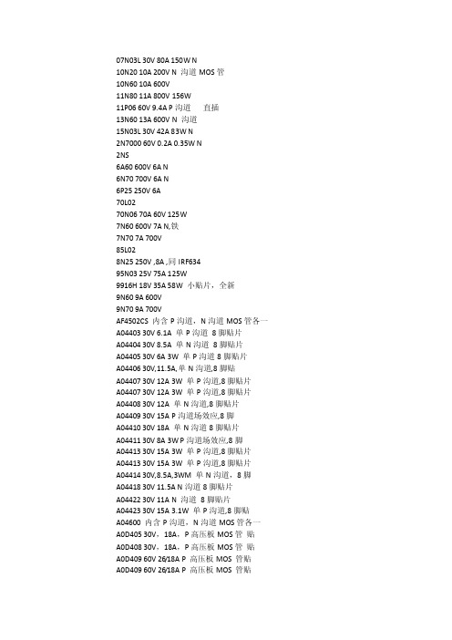
07N03L 30V 80A 150W N10N20 10A 200V N 沟道MOS管10N60 10A 600V11N80 11A 800V 156W11P06 60V 9.4A P沟道直插13N60 13A 600V N 沟道15N03L 30V 42A 83W N2N7000 60V 0.2A 0.35W N2NS6A60 600V 6A N6N70 700V 6A N6P25 250V 6A70L0270N06 70A 60V 125W7N60 600V 7A N,铁7N70 7A 700V85L028N25 250V ,8A ,同IRF63495N03 25V 75A 125W9916H 18V 35A 58W 小贴片,全新9N60 9A 600V9N70 9A 700VAF4502CS 内含P沟道,N沟道MOS管各一A04403 30V 6.1A 单P沟道8脚贴片A04404 30V 8.5A 单N沟道8脚贴片A04405 30V 6A 3W 单P沟道8脚贴片A04406 30V,11.5A,单N沟道,8脚贴A04407 30V 12A 3W 单P沟道,8脚贴片A04407 30V 12A 3W 单P沟道,8脚贴片A04408 30V 12A 单N沟道,8脚贴片A04409 30V 15A P沟道场效应,8脚A04410 30V 18A 单N沟道8脚贴片A04411 30V 8A 3W P沟道场效应,8脚A04413 30V 15A 3W 单P沟道,8脚贴片A04413 30V 15A 3W 单P沟道,8脚贴片A04414 30V,8.5A,3WM 单N沟道,8脚A04418 30V 11.5A N沟道8脚贴片A04422 30V 11A N 沟道8脚贴片A04423 30V 15A 3.1W 单P沟道,8脚贴A04600 内含P沟道,N沟道MOS管各一A0D405 30V,18A,P高压板MOS管贴A0D408 30V,18A,P高压板MOS管贴A0D409 60V 26/18A P 高压板MOS 管贴A0D409 60V 26/18A P 高压板MOS 管贴A0D420 30V,10A,N高压板MOS管贴A0D442 60V,38/27A,N 高压板MOS管贴A0D442 60V38/27A,N高压板MOS管贴A0D444 60V,12A,N 高压板MOS管贴A0P600 内含P,N沟道各1,30V 7.5AA0P605 内含P,N沟道各1,30V 7.5AA0P607 内含P、N沟道各1,60V 4。
EG8403 3W无滤波器D类立体声音频功放
ELECTRONIC GIANT EG8403芯片用户手册3W无滤波器D类立体声音频功放D类立体声音频功放版本变更记录D类立体声音频功放目录1. 特点 (3)2. 描述 (3)3. 应用领域 (3)4. 引脚 (4)4.1. 引脚定义 (4)4.2. 引脚描述 (4)5. 结构框图 (5)6. 典型应用电路 (5)6.1 EG8403典型应用电路图 (5)7. 电气特性 (6)7.1 极限参数 (6)7.2 典型参数 (6)7.3 热信息 (6)7.4 电气参数 (6)8. 应用信息 (8)8.1最大增益 (8)8.2静音工作模式 (8)8.3关断工作模式 (8)8.4电源退耦 (8)8.5输入电容 (8)8.6模拟基准旁路电容(C BYP) (9)8.7电源开启/关闭时噼噗噪声 (9)8.8欠压锁定(UVLO) (9)8.9短路电流保护(SCP) (9)8.10过温保护 (9)8.11电磁辐射(EMI) (10)9. 封装尺寸 (11)9.1 SOP16封装尺寸 (11)D类立体声音频功放EG8403芯片数据手册V1.01. 特点⏹无滤波器的D类放大器,低静态电流和低EMI⏹在4Ω负载和5V电源条件下,提供高达3W输出功率⏹效率高达90%⏹低THD,低噪声⏹短路电流保护⏹热保护⏹极少的外围元器件,节省空间和成本⏹封装形式: SOP16无铅封装2. 描述EG8403立体声D类音频功率放大器能够以D类放大器的效率提供AB类功率放大器的性能。
采用低噪声,无滤波器结构可以省去传统D类放大器的输出低通滤波器。
需要极少的外围元件,从而节省PCB的空间和系统成本,是便携式应用的理想选择。
EG8403能够以高于85%的效率提供3W功率,同时具有系统关断及静音控制功能。
特殊的线路架构增强了抗噪声能力,减少了射频干扰。
3. 应用领域⏹LCD电视、监视器⏹笔记本电脑⏹手机/免提电话⏹便携式DVD播放器,游戏机D 类立体声音频功放4. 引脚4.1. 引脚定义12345678161514131211109图4-1. EG8403管脚定义4.2. 引脚描述D类立体声音频功放5. 结构框图图5-1. EG8403结构框图6. 典型应用电路6.1 EG8403典型应用电路图图6-1. EG8403典型应用电路图D类立体声音频功放7. 电气特性7.1 极限参数注:超出所列的极限参数可能导致芯片内部永久性损坏,在极限的条件长时间运行会影响芯片的可靠性。
微波介质基板材料及选用
微波介质基板材料及选用微波介质基板是在微波电路设计和制造中广泛使用的一种重要材料。
它具有低介电损耗、高绝缘强度、良好的化学稳定性、低热膨胀系数和高温性能等特点。
基于不同的应用需求,选择适当的基板材料对于确保微波电路的性能至关重要。
本文将介绍几种常见的微波介质基板材料及其选用。
1.常见的介质基板材料:(1)FR4板:FR4是一种常见的玻纤增强热固性塑料,主要由玻璃纤维和环氧树脂组成。
它具有低成本、良好的机械性能和绝缘性能,因此被广泛应用于通信、计算机和消费电子等领域的微波电路设计。
(2)RO4003C板:RO4003C是一种高频率低介电损耗复合介质基板。
它由玻璃纤维增强PTFE(聚四氟乙烯)和陶瓷复合材料构成。
RO4003C具有较低的介电损耗、优秀的尺寸稳定性和化学稳定性,因此适用于高性能的射频和微波电路设计。
(3)RO4350B板:RO4350B是一种高频率低介电损耗复合介质基板。
它由玻璃纤维增强PTFE和陶瓷复合材料构成。
RO4350B具有较低的介电损耗、低热膨胀系数和优秀的维护性能,因此适用于高频率和高功率应用的微波电路设计。
(4)PTFE板:PTFE(聚四氟乙烯)是一种常见的高频率低介电损耗材料。
它具有优异的高温稳定性、化学稳定性和绝缘性能。
PTFE板常用于扩展频率范围和提高微波电路性能的特殊应用,如天线、传输线和滤波器等。
2.基于应用需求的选用:(1)频率要求:不同的基板材料具有不同的频率特性。
对于低频应用,如2.4GHzWLAN,FR4板就能满足需求。
而对于高频应用,如6GHzWLAN,RO4003C和RO4350B等低介电损耗基板将更适合。
(2)功率要求:高功率应用需要具备较好的热导性和绝缘性能,以确保电路的稳定性和性能。
RO4003C和RO4350B等陶瓷复合材料基板具有较低的热膨胀系数和较高的绝缘强度,适用于高功率应用。
(3)尺寸要求:一些特定领域的微波电路设计可能对尺寸稳定性和机械性能有较高的要求。
北京聚英翱翔电子有限公司 4路继电器板说明书
4路继电器板说明书
------双串口版产品功能及特点
7-30V宽电压供电
RS232、RS485(隔离)双串口通信方式
4路继电器手动控制
支持级联,1-32地址选择
接线方法
实物照片
地址选择:
1、五个拨码全都拨到“ON”位置时,为地址“1”;
2、五个拨码全都拨到“OFF”位置时,为地址“32”;
3、最左边1为二进制最低位。
通信协议
本产品可通过RS485总线,依照标准Modbus协议通信。
Modbus地址为00001-00004对应线圈1-4。
支持功能码1、5、15。
用户使用“16路继电器串口控制软件”或“16路继电器以太网口控制软件”对每一路进行手动控制
软件使用方法
软件界面
将产品通过串口与计算机连接,通过拨码开关设定地址(1-32),在设备地址一栏输入相对应的数值,选择正确串口及串口波特率(4路继电器板为38400,不可更改),点击打开串口,设备即可正常通信。
用户点击需要控制的某一路继电器开关,即可控制相应继电器的开闭。
按钮旁边的指示灯表示当前继电器状态,
常开触点闭合即亮红灯,否则为灰色。
该软件是为16路继电器板定制,所以,只有“继电器1”“继电器2”“继电器3”“继电器4”几个按键可用,5-16号继电器不可用,而且“打开全部”“关
闭全部”也不可用。
华为产品线划分、华为四大业务群整理
一、统一通讯 1.1 数据通讯产品 Quidway® AR46系列智能业务中心路由器 AR系列路由器 (中低端系列产 Quidway® AR28系列路由器 品) Quidway® AR18系列路由器 Quidway® NetEngine 5000E核心路由器 Quidway® NetEngine 80E核心路由器 NE系列路由器 Quidway® NetEngine 40E全业务路由器 (高端系列产品) Quidway® NetEngine 80核心路由器 Quidway® NetEngine 40系列通用交换路由器 Quidway® NetEngine 20/20E系列路由器 Quidway® S9300系列T比特路由交换机 Quidway® S8500系列万兆核心路由交换机 Quidway® S7800系列运营级汇聚交换机 Quidway® S6500系列高端多业务路由交换机 Quidway® S5600系列全千兆智能弹性交换机 以太网交换机 Quidway® S5300系列全千兆运营级交换机 Quidway® S3900系列智能弹性交换机 Quidway® S3500EA系列运营级园区交换机 Quidway® S3300系列运营级园区交换机 Quidway® S2300系列运营级接入交换机 Quidway® S2000TP-MI系列接入交换机 Quidway® S2000-EA系列运营级接入交换机 华为 Eudemon8000E 系列高端安全网关 华为Quidway Eudemon200E系列统一安全网关 华为Quidway SVN3000 安全接入网关 网络安全产品 SIG9280E/1000E SIG9800 DSM Secoway eLog CX系列城域业务平 Quidway® CX300系列城域业务平台 台 Quidway® CX200系列城域业务平台 Quidway® ME60系列 MSCG多业务控制网 Quidway® MA5200G系列 关 SmartAX® MA5200F系列 Quidway® RM9000系统 OptiX PTN 912 OptiX PTN 910 PTN OptiX PTN 950 OptiX PTN 1900 OptiX PTN 3900-8 OptiX PTN 3900 SRG系列业务路由 HUAWEI SRG1200系列业务路由网关 网关 HUAWEI SRG2200系列业务路由网关 HUAWEI SRG3200系列业务路由网关 1.2 视频产品 视讯 常用 常用
- 1、下载文档前请自行甄别文档内容的完整性,平台不提供额外的编辑、内容补充、找答案等附加服务。
- 2、"仅部分预览"的文档,不可在线预览部分如存在完整性等问题,可反馈申请退款(可完整预览的文档不适用该条件!)。
- 3、如文档侵犯您的权益,请联系客服反馈,我们会尽快为您处理(人工客服工作时间:9:00-18:30)。
RT8543®PreliminaryDS8543-P01 December 20121Copyright 2012 Richtek Technology Corporation. All rights reserved. is a registered trademark of Richtek Technology Corporation.©6-String 43V White LED Driver with Boost RegulatorGeneral DescriptionThe RT8543 is a high efficiency white LED driver. It is designed for LCD panel that employs an LED array as the lighting source. An integrated switch current mode Boost controller drives six strings in parallel and supports up to 10 pieces of LEDs per string. The internal current sinks support maximum ±2% current matching for excellent brightness uniformity in each LED string. T o provide enough headroom for the operating of current sink, Boost controller monitors the minimum voltage of feedback pins and regulates an optimized output voltage for power efficiency.The RT8543 has wide input voltage range from 2.5V to 24V and provides adjustable 5mA to 50mA LED current.The internal 200m Ω, 43V power switch with current-mode control provides cycle-by-cycle over current protection.The RT8543 also integrates PWM and analog dimming functions for accurate LED current control. The input PWM dimming frequency can operate from 100Hz to 20kHz without inducing any inrush current in LED or inductor.The RT8543 is available in thin WQFN-20L 4x4 package.Featuresz Wide Input Voltage : V IN 2.5V to 24Vz High Output Voltage : V OUT up to 43V zCurrent Mode Boost Regulator` 600kHz to 1.2MHz Switching Frequency ` Up to 85% High FrequencyzAdjustable Full Channel Current from 5mA to 50mA and Matched to 2%z Channel Current Regulation with ±3% Accuracy zDimming Controls` Direct PWM Dimming up to 20kHz and Minimum On-Time to 500ns` PWM to Analog Dimming up to 20kHz with 8 bit resolutionzBuilt-In Soft Start to Prevent Inrush Current without External Capacitorz Disconnects LED in Shutdown zProtection` Strings Open Detection ` Current Limit Protection` Adjustable Over Voltage Protection ` Over Temperature Protection z 20-Lead WQFN PackagezRoHS Compliant and Halogen FreeSimplified Application CircuitApplicationszUMPC and Notebook Computer Backlight2RT8543DS8543-P01 December 2012Preliminary©Copyright 2012 Richtek Technology Corporation. All rights reserved. is a registered trademark of Richtek Technology Corporation.Ordering InformationNote :Richtek products are :` RoHS compliant and compatible with the current require-ments of IPC/JEDEC J-STD-020.` Suitable for use in SnPb or Pb-free soldering processes.Pin ConfigurationsWQFN-20L 4x4(TOP VIEW)RT8543G : Green (Halogen Free and Pb Free)MODE ISET EN FREQ LX PGND OVP PGND L E D 6L E D 5L E D 3O M PI N W M D C XAGNDLED1L E D 2L E D 4Marking Information0N= : Product CodeYMDNN : Date Code3RT8543DS8543-P01 December 2012Preliminary©Copyright 2012 Richtek Technology Corporation. All rights reserved. is a registered trademark of Richtek Technology Corporation.Function Block DiagramOperationEnable ControlWhen VIN is higher than the UVLO voltage and the EN pin input voltage is higher than rising threshold, the VDC will be regulated around 3.8V if VIN is higher than 3.8V.OSCThe switching frequency is adjustable by the external resistor connected between the FREQ pin and GND.PWM ControllerThis controller includes some logic circuit to control LX N-MOSFET on/off. This block controls the minimum on-time and max duty of LX.OCP & OTPWhen LX N-MOSFET peak current is higher than 2.5A(typically), the LX N-MOSFET is turned off immediately and resumed again at next clock pulse. When the junction temperature is higher than 150°C (typically),the LX N-MOSFET will be turned off until the temperature is lower than the 120°C (typically).OVPWhen the OVP pin voltage is higher than 1.2V, the LX N-MOSFET is turned off immediately to protect the LX N-MOSFET .Minimum LED SelectionThis block detects all LEDx voltage and select a minimum voltage to EA (Error Amplifier). This function can guarantee the lowest of the LED pin voltage is around 600mV and Vout can be Boost to the highest forward voltage of LED strings.LED Open DetectionIf the voltage at LEDx pin is lower than 100mV, this channel is defined as open channel and the Minimum LED Selection function will discard it to regulate other used channels in proper voltage.……4RT8543DS8543-P01 December 2012Preliminary©Copyright 2012 Richtek Technology Corporation. All rights reserved. is a registered trademark of Richtek Technology Corporation.Electrical CharacteristicsRecommended Operating Conditions (Note 4)z Supply Input Voltage, VIN -----------------------------------------------------------------------------------------------2.5V to 24V z Junction T emperature Range --------------------------------------------------------------------------------------------−40°C to 125°C zAmbient T emperature Range --------------------------------------------------------------------------------------------−40°C to 85°CAbsolute Maximum Ratings (Note 1)z Supply Input Voltage, VIN to GND ------------------------------------------------------------------------------------−0.3V to 26.5V z EN, PWM, ISET , COMP , MODE, FREQ to GND ------------------------------------------------------------------−0.3V to 26.5V z LX, OVP , LED1 to LED6 to GND ---------------------------------------------------------------------------------------−0.3V to 48V z VDC to GND ----------------------------------------------------------------------------------------------------------------−0.3V to 7V zPower Dissipation, P D @ T A = 25°CWQFN −20L 4x4------------------------------------------------------------------------------------------------------------3.57W zPackage Thermal Resistance (Note 2)WQFN −20L 4x4, θJA ------------------------------------------------------------------------------------------------------28°C/W WQFN −20L 4x4, θJC ------------------------------------------------------------------------------------------------------7°C/W z Lead Temperature (Soldering, 10 sec.)-------------------------------------------------------------------------------260°C z Junction T emperature -----------------------------------------------------------------------------------------------------150°Cz Storage T emperature Range --------------------------------------------------------------------------------------------−65°C to 150°C zESD Susceptibility (Note 3)HBM (Human Body Model)----------------------------------------------------------------------------------------------2kV MM (Machine Model)-----------------------------------------------------------------------------------------------------200V5RT8543DS8543-P01 December 2012Preliminary©Copyright 2012 Richtek Technology Corporation. All rights reserved. is a registered trademark of Richtek Technology Corporation.Note 1. Stresses beyond those listed “Absolute Maximum Ratings ” may cause permanent damage to the device. These arestress ratings only, and functional operation of the device at these or any other conditions beyond those indicated in the operational sections of the specifications is not implied. Exposure to absolute maximum rating conditions may affect device reliability.Note 2. θJA is measured at T A = 25°C on a high effective thermal conductivity four-layer test board per JEDEC 51-7. θJC ismeasured at the exposed pad of the package.Note 3. Devices are ESD sensitive. Handling precaution is recommended.Note 4. The device is not guaranteed to function outside its operating conditions.6RT8543DS8543-P01 December 2012Preliminary©Copyright 2012 Richtek Technology Corporation. All rights reserved. is a registered trademark of Richtek Technology Corporation.Typical Application CircuitFigure 1. For General Application CircuitFigure 2. For Low Input Voltage Application CircuitOUTL1D1L1D1V OUT25V MAX(V OUT depends on D MAX )7RT8543DS8543-P01 December 2012Preliminary©Copyright 2012 Richtek Technology Corporation. All rights reserved. is a registered trademark of Richtek Technology Corporation.OVP Threshold Voltage vs. Input Voltage1.01.11.21.31.41.54812162024Input Voltage (V)O V P T h r e s h o l d V o l t a g e (V)Typical Operating CharacteristicsLED Driver Efficiency020406080100102030405060708090100Dimming Duty (%)E f f i c i e n c y (%)LED Current vs. Temperature1819202122-50-25255075100125Temperature (°C)L E D C u r r e n t (m A)LED Current vs. Input Voltage18192021224812162024Input Voltage V IN (V)L E D C u r r e n t (m A )LED Current vs. PWM Duty Cycle04812162020406080100PWM Duty Cycle (%)L E D C u r r e n t (m A)Quiescent Current vs. Input Voltage1.51.82.02.32.52.57.011.516.020.525.0Input Voltage (V)Q u i e s c e n t C u r r e n t(m A )8RT8543DS8543-P01 December 2012Preliminary©Copyright 2012 Richtek Technology Corporation. All rights reserved. is a registered trademark of Richtek Technology Corporation.Time (10ms/Div)Power On Mixed Mode1V IN = 12V, 60 LEDs, R ISET = 49.9k ΩEN (5V/Div)V IN (10V/Div)PWM (5V/Div)I LED(100mA/Div)Time (10ms/Div)Power On PWM Mode EN (5V/Div)V IN (10V/Div)PWM (5V/Div)I LED(50mA/Div)V IN = 12V, 60 LEDs, R ISET = 49.9k ΩTime (10ms/Div)Power On Mixed Mode2V IN = 12V, 60 LEDs, R ISET = 49.9k ΩEN (5V/Div)V IN (10V/Div)PWM (5V/Div)I LED(100mA/Div)Time (5ms/Div)Power On from ENEN (5V/Div)V LED (20V/Div)LX (20V/Div)I IN(500mA/Div)V IN = 12V, 60 LEDs, R ISET = 49.9k ΩV IN = 5V to 13V, R ISET = 49.9k ΩTime (50ms/Div)LED Line Transient Response I LED(10mA/Div)V IN (5V/Div)Time (10ms/Div)Power On Mixed Mode3V IN = 12V, 60 LEDs, R ISET = 49.9k ΩEN (5V/Div)V IN (10V/Div)PWM (5V/Div)I LED(100mA/Div)9RT8543DS8543-P01 December 2012Preliminary©Copyright 2012 Richtek Technology Corporation. All rights reserved. is a registered trademark of Richtek Technology Corporation.Application InformationThe RT8543 is a general purpose 6-CH LED driver capable of delivering an adjustable 5mA to 50mA LED current. The IC is a current mode Boost converter integrated with a 43V/2.5A power switch and can cover a wide VIN range from 2.5V to 24V. The part integrates built-in soft-start with PWM dimming control provides over voltage, over temperature and current limit protection features. It also integrates PWM and mixed mode dimming function for accurate LED current control. The PWM dimming frequency can operate from 100Hz to 20kHz without inducing any inrush current in LED or inductor.LED Power Soft-Start FunctionThe period from EN is enabled to LED current rises, is several tens of milliseconds according to the brightness dimming mode (PWM Mode or Mixed Mode). The LED current starts up after VIN, PWM and EN signals are all ready. The RT8543 supports soft-start function to reduce inrush current, and the soft-start inrush peak current must be less than 2.5A.LED Driver CompensationThe control loop can be compensated by adjusting the external components connected to the COMP pin. The COMP pin is the output of the internal error amplifier. The compensation capacitors, C C and C COMP , will adjust the zero and pole respectively to maintain stability. Moreover,the resistor, R COMP , will adjust the mid-band gain for fast transient response.Setting and Regulation of LED CurrentThe LED current can be calculated by the following equation :LED ISET 1000I (mA)R =where, R ISET is the resistor between the ISET pin and GND. This setting is the reference for the LED current at LED1 to LED6 and represents the sensed LED current for each string. The DC/DC converter regulates the LED current according to the setting.LED Driver Inductor SelectionThe value of the inductor (L) calculated by the following equation determines the criteria of the transition from DCM to CCM mode :()2OUT IN IN 2OUT SW OUT V V V L 2I f V −×=×××()OUT OUT IN SW OUT IN PEAK IN OUT V I V T V V I V 2L V ×⎛⎞×−⎛⎞=+×⎜⎟⎜⎟××⎝⎠⎝⎠ηwhere,V OUT is the maximum output voltage.V IN is the minimum input voltage.f SW is the switching frequency.I OUT is the sum of current from all LED strings.The LED Boost converter operates in DCM over the entire input voltage range when the inductor value L1 is less than this value L. With an inductance greater than L, the converter operates in CCM at the minimum input voltage and may be discontinuous at higher voltages. The inductor must be selected with saturation current rating greater than the peak current calculated by the following equation :LED Driver Diode SelectionSchottky diode is a good choice for any asynchronousBoost converter due to its small forward voltage and fast switching speed. However, when selecting a Schottky diode, important parameters such as power dissipation,reverse voltage rating and pulsating peak current must all be taken into consideration. Choose a suitable diode with reverse voltage rating greater than the maximum output voltage.LED Driver Capacitor SelectionThe input capacitor reduces current spikes from the input supply and minimizes noise injection to the converter. For most applications, a 4.7μF ceramic capacitor is sufficient.A value higher or lower may be used depending on the noise level from the input supply and the input current to the converter. It is recommended to choose a ceramic10RT8543DS8543-P01 December 2012Preliminary©Copyright 2012 Richtek Technology Corporation. All rights reserved. is a registered trademark of Richtek Technology Corporation.()OUT IN OUTOUT RIPPLE OUT SWV V I C V V f η−×=×××PWM Mode / Mixed Mode and Pure DC Mode Brightness DimmingThe RT8543 allows three ways of LED brightness control.PWM Mode Dimming : When the MODE pin is set to float, the dimming mode operates in PWM Mode (Figure 3). During the PWM dimming, the current source turn-on/off is synchronized with the PWM signal. The LED current frequency is equivalent to PWM input frequency.Mixed Mode Dimming : If the MODE pin is set to GND,the dimming mode operates in Mixed Mode (Figure 4). In this mode, the PWM and I OUT dimming cycle will delay by two periods. First cycle delay is required for the period,while the second cycle delay is for the duty rate calculation.(a) When 25% ≤ PWM duty ≤ 100%, the current source outputs are DC dimming, and the PWM duty cycle modulates the amplitude of the currents.(b) PWM Duty < 25%, the DC dimming will translate to DC-PWM dimming to control the LED current. In this state,the LED current is fixed at 0.25 x I SET , and the dimming duty is 4 x PWM duties.Pure DC Mode Dimming : If the MODE pin is set to VDC,the PWM and I OUT will delay by two periods. First cycle delay is required for the period, while the second cycle delay is for the duty rate calculation.The minimum D/A converter is 512 steps resolution for I SET regulation.Figure 3. LED Current Control Using PWM DimmingMode (MODE = Floating)Figure 4. LED Current Control Using Mixed DimmingMode (MODE = GND)Figure 5. LED Current Control Using Pure DC DimmingMode (MODE = VDC)PWMI SETI OUTOAII capacitor based on the output voltage ripple requirements.The minimum value of the output capacitor, C OUT , can be calculated by the following equation :DS8543-P01 December 2012©Copyright 2012 Richtek Technology Corporation. All rights reserved. is a registered trademark of Richtek Technology Corporation.Figure 6. LED UVLO FunctionFigure 7. LED Driver Power On Sequence (PWM Mode)VINENV OUTI OUTBrightness ControlThe RT8543 features the digital dimming control scheme.A very high contrast ratio true digital PWM dimming can be achieved by driving PWM pin with a the PWM signal and the recommended PWM frequency is 100Hz to 10kHz. Dimming frequency can be sufficiently adjusted from 100Hz to 20kHz. However, LED current cannot be 100% proportional to duty cycle especially for high frequency and low duty ratio because of physical limitation caused by inductor rising time. Please refer to Table 1,Table 2 and Table 3.Table 1. Mixed Dimming ModeTable 3. DC Dimming ModeNote : The minimum duty in Table 1 and Table 2 is based on the application circuit and does not consider the deviation of current linearity when f PWM > 10kHz, ILED may not achieve setting current in duty (min.) due to different VOUT / VIN ratio at V IN = 12V.LED Driver Under Voltage Lockout (UVLO)The UVLO circuit compares the LED driver input voltage at VIN with the UVLO threshold (2.3V rising, typ.) to ensure the input voltage is high enough for reliable operation.The 200mV (typ.) hysteresis prevents supply transients from causing a shutdown. Once VIN exceeds the UVLO rising threshold, the LED soft-start will begin after a delaytime around several milliseconds. When VIN falls below the UVLO falling threshold, the controller turns off all LED driver functions.Figure 8. LED Driver Power On Sequence (Mixed Mode)V I VIN PWM ENV OUT I OUTV I Figure 9. LED Driver Power On Sequence (Mixed Mode;Duty = 100%)©Copyright 2012 Richtek Technology Corporation. All rights reserved. is a registered trademark of Richtek Technology Corporation.Figure 10. Derating Curve of Maximum PowerDissipation LED Channel Open Circuit ProtectionIf at least one channel is in normal operation, the LED driver will automatically ignore the open channels and continue to regulate current for the channels in normal operation.LED Driver Over Voltage ProtectionThe LED driver equips an Over Voltage Protection (OVP)function. When the voltage at the OVP pin reaches a threshold of approximately 1.2V, the driver will turn off.The drivers turn on again once the voltage at OVP drops below the threshold voltage. Thus, the output voltage can be clamped at a certain voltage level. This voltage level can be calculated by the following equation :OVP2OUT, OVP OVP OVP1R V V 1R ⎛⎞=×+⎜⎟⎝⎠where R OVP1 and R OVP2 are the resistors in the voltagedivider connected to close to the OVP pin. It is suggested to use 1M Ω for R OVP2 to reduce loading effect.Over Temperature ProtectionThe RT8543 includes an Over Temperature Protection (OTP) feature to prevent overheating due to excessive power dissipation from damaging the device. The OTP function will shut down LED driver when the junction temperature exceeds 150°C. It will reactivate the device when powered on again. T o maintain continuous operation,the junction temperature should be kept below 125°C.Thermal ConsiderationsFor continuous operation, do not exceed absolute maximum junction temperature. The maximum power dissipation depends on the thermal resistance of the IC package, PCB layout, rate of surrounding airflow, and difference between junction and ambient temperature. The maximum power dissipation can be calculated by the following formula :P D(MAX) = (T J(MAX) − T A ) / θJAwhere T J(MAX) is the maximum junction temperature, T A is the ambient temperature, and θJA is the junction to ambient thermal resistance.For recommended operating condition specifications, the maximum junction temperature is 125°C. The junction toambient thermal resistance, θJA , is layout dependent. For WQFN-20L 4x4 package, the thermal resistance, θJA , is 28°C/W on a standard JEDEC 51-7 four-layer thermal test board. The maximum power dissipation at T A = 25°C can be calculated by the following formula :P D(MAX) = (125°C − 25°C) / (28°C/W) = 3.57W for WQFN-20L 4x4 packageThe maximum power dissipation depends on the operating ambient temperature for fixed T J(MAX) and thermal resistance, θJA . The derating curve in Figure 10 allows the designer to see the effect of rising ambient temperature on the maximum power dissipation.0.00.81.62.43.24.0255075100125Ambient Temperature (°C)M a x i m u m P o w e r D i s s i p a t i o n (W )Layout ConsiderationsPCB layout is very important to design power switching converter circuits. The following layout guide lines should be strictly followed for best performance of the RT8543.`The power components L1, D1, C IN and C OUT must be placed as close as possible to reduce the ac current loop. The PCB trace between power components must be short and wide as possible due to large current flow through these trace during operation.`Place L1 and D1 connected to LX pins as close as possible. The trace should be short and wide as possible.`It is recommend to place C1 close to VIN pin.`Pin 20 is the compensation point to adjust system stability. Place the compensation components to pin 20 as close as possible.Copyright 2012 Richtek Technology Corporation. All rights reserved. is a registered trademark of Richtek Technology Corporation.DS8543-P01 December W-Type 20L QFN 4x4 PackageRichtek Technology Corporation5F, No. 20, Taiyuen Street, Chupei CityHsinchu, Taiwan, R.O.C.Tel: (8863)5526789Richtek products are sold by description only. Richtek reserves the right to change the circuitry and/or specifications without notice at any time. Customers should obtain the latest relevant information and data sheets before placing orders and should verify that such information is current and complete. Richtek cannot assume responsibility for use of any circuitry other than circuitry entirely embodied in a Richtek product. Information furnished by Richtek is believed to be accurate and reliable. However, no responsibility is assumed by Richtek or its subsidiaries for its use; nor for any infringements of patents or other rights of third parties which may result from its use. No license is granted by implication or otherwise under any patent or patent rights of Richtek or its subsidiaries.Copyright 2012 Richtek Technology Corporation. All rights reserved. is a registered trademark of Richtek Technology Corporation.DS8543-P01 December 。