RT9297富佳维
富捷电子 RT9296 3x3同步增压转换器数据手册说明书

1DS9296-01 April 2011Note :Richtek products are :` RoHS compliant and compatible with the current require-ments of IPC/JEDEC J-STD-020.` Suitable for use in SnPb or Pb-free soldering processes.Ordering InformationPin Configurations(TOP VIEW)WDFN-10L 3x3Synchronous Boost Converter with LDO ControllerGeneral DescriptionThe RT9296 is a synchronous boost converter, which is based on a fixed frequency pulse-width-modulation (PWM)controller using a synchronous rectifier to obtain maximum efficiency. The converter provides a power supply solution for products powered by a variety of batteries such as single cell, dual cell alkaline, NiMH and NiCd battery. At light load currents, the converter enters the power save mode to maintain a high efficiency over a wide load current range.The output voltage can be programmed by an external resistor divider, or be a fixed voltage. Moreover, the converter can be disabled to the minimize battery drain.During shutdown, the load is completely disconnected from the battery. The maximum peak current in the boost switch is limited to 2A for current limit.For the RT9296, a low-EMI (anti-ringing) mode is implemented (by trim option) to reduce ringing of the inductor phase pin when the converter enters the discontinuous conduction mode. Moreover, a linear controller is built-in in the chip for linear regulator application.Featuresz True Load Disconnection During Shutdown z Internal Synchronous Rectifier z Up to 96% EfficiencyzCurrent Mode PWM Operation with Internal Compensationz Low Start-Up Voltage z Low Quiescent Current z Internal Soft-Start Control z Linear Controllerz Low EMI Converter (Anti-Ringing)zPower Save Mode for Improved Efficiency at Light Load Currentz Over-Current Protection z Short Circuit Protectionz Over Temperature Protection z Over Voltage Protectionz Small 10-Lead WDFN PackagezRoHS Compliant and Halogen FreeApplicationszAll One-Cell, Two-Cell and Three-Cell Alkaline, NiCd,NiMH and Single-Cell Li Batteries z Hand-Held Devices zWLED Flash LightMarking InformationFor marking information, contact our sales representative directly or through a Richtek distributor located in your area.PGND LXVBATFBLPGOOD Boost VOUTDefault : Adjustable 33 : 3.3V 50 : 5.0VRT9296(2DS9296-01 April 2011Typical Application CircuitFigure 2. Adjustable Output Voltage Boost Converter with WLED DriverFigure 1. Fixed Output Voltage Boost Converter with Linear RegulatorOUTOUT3DS9296-01 April 2011Function Block DiagramFigure 3. Fixed Voltage RegulatorFigure 4. Adjustable Voltage Regulator4DS9296-01 April 2011 Electrical Characteristics(V2.5V or V = V + 0.7V, V = V , C = 10μF, C = 22μF, T = 25°C, unless otherwise specified)To be continuedRecommended Operating Conditions (Note 4)z Supply Input Voltage Range, V BAT -------------------------------------------------------------------------------------1.2V to 5Vz Junction T emperature Range --------------------------------------------------------------------------------------------−40°C to 125°C zAmbient T emperature Range --------------------------------------------------------------------------------------------−40°C to 85°CAbsolute Maximum Ratings (Note 1)z Supply Input Voltage, V BAT ----------------------------------------------------------------------------------------------−0.3V to 6V z Boost Output Voltage, V OUT --------------------------------------------------------------------------------------------−0.3V to 6.5V z Switch Output Voltage, LX ----------------------------------------------------------------------------------------------−0.3V to 6.5V z Digital Input Voltage, EN, FBL -----------------------------------------------------------------------------------------−0.3V to 6V z Digital Output Voltage, DRV, PGOOD --------------------------------------------------------------------------------−0.3V to 6V z Others Pin-------------------------------------------------------------------------------------------------------------------−0.3V to 6V zPower Dissipation, P D @ T A = 25°CWDFN-10L 3x3-------------------------------------------------------------------------------------------------------------1.429W zPackage Thermal Resistance (Note 2)WDFN-10L 3x3, θJA -------------------------------------------------------------------------------------------------------70°C/W WDFN-10L 3x3, θJC -------------------------------------------------------------------------------------------------------7.8°C/W z Junction T emperature Range --------------------------------------------------------------------------------------------150°C z Lead Temperature (Soldering, 10 sec.)-------------------------------------------------------------------------------260°Cz Storage T emperature Range --------------------------------------------------------------------------------------------−65°C to 150°C zESD Susceptibility (Note 3)HBM (Human Body Mode)----------------------------------------------------------------------------------------------2kV MM (Machine Mode)------------------------------------------------------------------------------------------------------200V5DS9296-01 April 2011Note 1. Stresses listed as the above "Absolute Maximum Ratings" may cause permanent damage to the device. These are forstress ratings. Functional operation of the device at these or any other conditions beyond those indicated in the operational sections of the specifications is not implied. Exposure to absolute maximum rating conditions for extended periods may remain possibility to affect device reliability.Note 2. θJA is measured in the natural convection at T A = 25°C on a high effective four layers thermal conductivity test board ofJEDEC 51-7 thermal measurement standard. The case point of θJC is on the expose pad for the WDFN package.Note 3. Devices are ESD sensitive. Handling precaution is recommended.Note 4. The device is not guaranteed to function outside its operating conditions.6DS9296-01 April 2011 Efficiency vs. Load Current1020304050607080901000.0010.010.11Load Current (A)E f f i c i e n c y (%)Efficiency vs. Load Current1020304050607080901000.0010.010.11Load Current (A)E f f i c i e n c y (%)Efficiency vs. Input Voltage0.91.41.92.42.93.4Input Voltage (V)E f f i c i e n c y (%)Efficiency vs. Input Voltage0.91.41.92.42.93.43.94.44.9Input Voltage (V)E f f i c i e n c y (%)Output Voltage vs. Load Current3.003.053.103.153.203.253.303.353.400.0010.010.11Load Current (A)O u t p u t V o l t a g e (V )Output Voltage vs. Load Current4.54.64.74.84.95.05.10.0010.010.11Load Current (A)O u t p u t V o l t a g e (V )Typical Operating Characteristics7DS9296-01 April 2011Output Voltage vs. Input Voltage2.02.53.03.54.04.55.05.56.00.91.41.92.42.93.43.94.44.9Input Voltage (V)O u t p u t V o l t a g e (V )Switching Frequency vs. Temperature9009501000105011001150120012501300-50-25255075100125Temperature S wi t c h i n g F re q u e n c y (k H z )FB Reference Voltage vs. Temperature0.450.460.470.480.490.500.510.520.530.540.55-50-25255075100125Temperature F B R e f e r e n c e V o l t a g e (V )FBL Reference Voltage vs Temperature0.150.160.170.180.190.200.210.220.230.240.25-50-25255075100125Temperature F B L R e f e r e n c e V o l t a g e (V )(°C)(°C)(°C)DCM Switching I LX(200mA/Div)V IN (2V/Div)Time (1μs/Div)V BAT = 3.6V, V OUT = 5V, I LOAD = 20mAV OUT (20mV/Div)CCM SwitchingI LX(500mA/Div)V IN (2V/Div)Time (250ns/Div)V BAT = 3.6V, V OUT = 5V, I LOAD = 200mAV OUT (50mV/Div)V LX (5V/Div)8DS9296-01 April 2011 Load Transient ResponseI OUT(200mA/Div)V IN (2V/Div)Time (500μs/Div)V BAT = 3.6V, V OUT = 5V, I LOAD = 100mA to 200mAV OUT(100mV/Div)Line Transient ResponseI OUT(200mA/Div)V IN (2V/Div)Time (500μs/Div)V BAT = 3V to 3.6V, V OUT = 5V, I LOAD = 200mAV OUT(100mV/Div)9DS9296-01 April 2011Application InformationThe RT9296 integrates a high-efficiency synchronous step-up DC-DC converter and a linear regulator controller. To fully utilize its advantages, peripheral components should be appropriately selected. The following information provides detailed description of application.Inductor SelectionFor a better efficiency in high switching frequency converter, the inductor selection has to use a proper core material such as ferrite core to reduce the core loss and choose low ESR wire to reduce copper loss. The most important point is to prevent the core saturation when handling the maximum peak current. Using a shielded inductor can minimize radiated noise in sensitive applications. The maximum peak inductor current is the maximum input current plus the half of inductor ripple current. The calculated peak current has to be smaller than the current limitation in the electrical characteristics.A typical setting of the inductor ripple current is 20% to 40% of the maximum input current. If the selection is 40%The minimum inductance value is derived from the followingequation :Depending on the application, the recommended inductorvalue is between 2.2μH and 10μH.Input Capacitor SelectionFor better input bypassing, low-ESR ceramic capacitors are recommended for performance. A 10μF input capacitor is sufficient for most applications. For a lower output power requirement application, this value can be decreased Output Capacitor SelectionFor lower output voltage ripple, low-ESR ceramic capacitors are recommended. The tantalum capacitors can be used as well, but the ESR is bigger than ceramic capacitor. The output voltage ripple consists of two components: one is the pulsating output ripple currentOutput Voltage SettingReferring to application circuit (Figure 2), the output voltage of the switching regulator (V OUT ) can be set with below equation :where V FB = 0.5V (typ.)Linear RegulatorThe RT9296 integrates a linear controller with an open-drain output. An external P-MOSFET and external feedback resistors are required for this application. The feedback voltage is set at 0.2V typically.For linear regulator application, the output voltage can be set by an external voltage resistive divider. For WLED driver application, the LED current can be set by an external feedback resistor.Thermal ConsiderationsFor continuous operation, do not exceed absolute maximum operation junction temperature. The maximum power dissipation depends on the thermal resistance of IC package, PCB layout, the rate of surroundings airflow and temperature difference between junction to ambient.The maximum power dissipation can be calculated by following formula :P D(MAX) = (T J(MAX) − T A ) / θJAWhere T J(MAX) is the maximum operation junction temperature, T A is the ambient temperature and the θJA is the junction to ambient thermal resistance.For recommended operating conditions specification of RT9296, the maximum junction temperature is 125°C . The junction to ambient thermal resistance θJA is layout dependent. For WDFN-10L 3x3 packages, the thermal resistance θJA is 70°C /W on the standard JEDEC 51-7four layers thermal test board. The maximum power dissipation at T A = 25°C can be calculated by followingPK IN(MAX)RIPPLE IN(MAX)OUT(MAX)OUT IN(MIN)1I I I 1.2I 2I V 1.2V η=+=×⎡⎤×=×⎢⎥×⎣⎦[]22IN(MIN)OUT IN(MIN)OUT(MAX)OUT SWI V V L 0.4I V f η××−=×××RIPPLE RIPPLE(ESR)RIPPLE(C)PEAK OUT IN PEAK ESR OUT OUT SW V V V I V V I R C V f =+−⎡⎤≅×+⎢×⎣⎦OUT FBR1V 1V R2⎛⎞=+×⎜⎟⎝⎠flows through the ESR, and the other is the capacitive ripple caused by charging and discharging.10DS9296-01 April 2011 Figure 5. Derating Curves for RT9296 Packages Layout ConsiderationFor Best performance of RT9296, the following layout guidelines must be strictly followed.`Input and Output capacitors should be placed close to the IC and connected to ground plane to reduce noise coupling.`The GND and Exposed Pad should be connected to a strong ground plane for heat sinking and noise protection.`Keep the main current traces as possible as short and wide.`Place the feedback components as close as possible to the IC and keep away from the noisy devices.formula :P D(MAX) = (125°C − 25°C ) / (70°C /W) = 1.429W for WDFN-10L 3x3 packagesThe maximum power dissipation depends on operating ambient temperature for fixed T J(MAX) and thermal resistance θJA . For RT9296 packages, the Figure 5 of derating curves allows the designer to see the effect of rising ambient temperature on the maximum power allowed.0.00.20.40.60.81.01.21.41.6255075100125Ambient Temperature (°C)M a x i m u m P o w e r D i s s i p a t i o n (W )Figure 6. PCB Layout Guidearea should be pin)C IN and C OUT should be placed close to the IC and connected to ground plane to reduce connected to a strong ground plane for heat sinking and noise protection.11DS9296-01 April 2011Information that is provided by Richtek Technology Corporation is believed to be accurate and reliable. Richtek reserves the right to make any change in circuit design, specification or other related things if necessary without notice at any time. No third party intellectual property infringement of the applications should be guaranteed by users when integrating Richtek products into any application. No legal responsibility for any said applications is assumed by Richtek.Richtek Technology CorporationHeadquarter5F, No. 20, Taiyuen Street, Chupei City Hsinchu, Taiwan, R.O.C.Tel: (8863)5526789 Fax: (8863)5526611Richtek Technology CorporationTaipei Office (Marketing)5F, No. 95, Minchiuan Road, Hsintien City Taipei County, Taiwan, R.O.C.Tel: (8862)86672399 Fax: (8862)86672377Email:*********************W-Type 10L DFN 3x3 Package。
HSP 94107
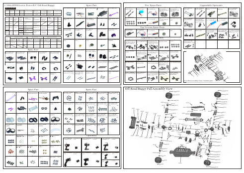
102048-Aluminum Nut M3
103009-Aluminum Battery Posts+Flat Head Machine3*10*2P
3*8
3*8
3*10
3*10
3*10
0200322078
3*12
3*11 3*15
4*4
3*15
102049-Aluminum Nut M4
106617-Front/Rear & 106619-Front Lower Arm 106621-Rear Lower Arm
26mm
86mm
32mm(R) 29mm(F)
GEAR RATIO 1:8.133
Styles
KV
Motor (Brushless Motor)
Motor RPM range
Brush Version Rc540
20000rpm
Brushless 3650 Version (RC540)
3300KV
Motor Gear
Gear Ratio
PRO1.GEAR
Diff.Main
Gear
Motor Gear
Gear Ratio
PRO2.GEAR(Metal)
Diff.Main
Gear
Gear
Motor Gear Ratio
#11164-64T #11153-23T 1:8.133 #11188-48T #11177-17T 1:8.25 #11184-64T #11176-26T 1:7.195
ESC Specification
Continue Forward150A/ Continue outward100A
Bosch GSN29UW3V NoFrost 161 x 60 cm diepvriezer 商品

Serie | 4, vrijstaande diepvriezer, 161 x 60 cm,GSN29UW3VDe NoFrost diepvriezer met FreshSense:beschermt uw diepvrieswaren door eenconstante diepvriestemperatuur.Technische gegevensTemperatuur in display vriezer : DigitaalVerlichting : NeenProductcategorie : VrieskastUitvoering : VrijstaandMeubeldeur opties : Niet mogelijkNo-frost systeem : Koelkast en vriezerHoogte van het apparaat : 1610 mmBreedte apparaat : 600 mmDiepte apparaat : 650 mmAfmetingen inclusief verpakking hxbxd : 1680 x 765 x 660 mmNettogewicht : 67,846 kgBrutogewicht : 74,1 kgAansluitwaarde : 90 WMinimale smeltveiligheid : 10 AFrequentie : 50 HzKeurmerken : CE, VDELengte elektriciteitssnoer : 230 cmDeurscharnier : Rechts verwisselbaarMaximale bewaarduur bij stroomuitval (uren) : 25 hKleur en materiaal ombouw : WhiteAlarmsignaal bij storing : Optisch en akoestischDeur afsluitbaar : NeenAantal vriesladen/manden : 5Aantal vriesvakken met klep : 1EAN-code : 4242005051946Merk : BoschProductnaam : GSN29UW3VProductcategorie : VrieskastEnergieverbruik - NIEUW (2010/30/EG) : 214,00 kWh/annumNetto inhoud - nieuw (2010/30/EC) : 200 lInvriescapaciteit in 24 uur - nieuw (2010/30/EC) : 20 kg/24hKlimaatklasse : SN-TGeluidsniveau : 42 dBType installatie : n.v.t'!2E20A F-a f b j e g!1/3Serie | 4, vrijstaande diepvriezer, 161 x 60cm,GSN29UW3VDe NoFrost diepvriezer met FreshSense:beschermt uw diepvrieswaren door eenconstante diepvriestemperatuur.Algemene informatie-NoFrost - nooit meer ontdooien-Energie-efficiëntieklasse A++ op een schaal van energie-efficiëntieklassen van A+++ tot D-Energie-efficiëntieklasse A++ op een schaal van energie-efficiëntieklassen van A+++ tot D : 214 kWu/jaar-Totale netto-inhoud: 200 l-Invriesvermogen: 20 kg in 24 uur-Bewaartijd bij stroomonderbreking: 25 u-Geluidsniveau: 42 dB(A) re 1 pWUitrusting-Deuren Wit, zijwanden Wit-Verticale handgreep-Elektronische temperatuurregeling, afleesbaar via LED-Actief waarschuwingssysteem met optisch en akoestischalarm bij temperatuurtoename-FreshSense - constante temperatuur met intelligentesensortechnologieDiepvriesgedeelte-Schakelaar voor supervriezen: Manual/automatic activiation-MultiAirflow-systeem-VarioZone - uitneembare glazen legplateaus voor extra ruimte!-5 transparante diepvriesladen, waarvan 1 BigBoxToebehoren-Koude accu'sAfmetingen-Afmetingen toestel (H x B x D): 161 x 60 x 65 cm-Deuropening 90°Technische informatie-Draairichting deur rechts, verwisselbaar-In de hoogte verstelbare voetjes vooraan, rolwieltjes achteraan-Aansluitwaarde: 90 W-Netspanning 220 - 240 V-Klimaatklasse: SN-T2/3Serie | 4, vrijstaande diepvriezer, 161 x 60cm,GSN29UW3V3/3。
Motorola 3.5 kHz 产品说明书
RVN4126 3.59100-386-9100-386/T DEVICERVN41772-CD2-3.5MCS/MTSRVN41821-CD2-3.5XTS3000/SABER PORTABLE YES RKN4046KHVN9085 3.51-20 R NO HLN9359 PROG. STAND RVN4057 3.532 X 8 CODEPLUG NO3080385B23 & 5880385B30 MDVN4965 3.59100-WS/T CONFIG KITRVN4053 3.5ASTRO DIGITAL INTERFACE NO3080385B23RVN41842-CD RKN4046A (Portable) 2-3.5ASTRO PORTABLE /MOBILE YES3080369B73 or0180300B10 (Mobile) RVN41831-CD3080369B732-3.5ASTRO SPECTRA MOBILE YES(Low / Mid Power)0180300B10 (High Power) RVN4185CD ASTRO SPECTRA PLUS MOBILE NO MANY OPTIONS; SEESERVICE BRIEF#SB-MO-0101RVN4186CD ASTRO SPECTRA PLUS MANY OPTIONS;MOBILE/PORTABLE COMB SEE SERVICE BRIEF#SB-MO-0101RVN4154 3.5ASTROTAC 3000 COMPAR.3080385B23RVN5003 3.5ASTROTAC COMPARATORS NO3080399E31 Adpt.5880385B34RVN4083 3.5BSC II NO FKN5836ARVN4171 3.5C200RVN4029 3.5CENTRACOM SERIES II NO VARIOUS-SEE MANUAL6881121E49RVN4112 3.5COMMAND PLUS NORVN4149 3.5COMTEGRA YES3082056X02HVN6053CD CT250, 450, 450LS YES AAPMKN4004RVN4079 3.5DESKTRAC CONVENTIONAL YES3080070N01RVN4093 3.5DESKTRAC TRUNKED YES3080070N01RVN4091 3.5DGT 9000 DESKSET YES0180358A22RVN4114 3.5GLOBAL POSITIONING SYS.NO RKN4021AHVN8177 3.5GM/GR300/GR500/GR400M10/M120/130YES3080070N01RVN4159 3.5GP60 SERIES YES PMLN4074AHVN9128 3.5GP300 & GP350RVN4152 3.5GP350 AVSRVN4150 3.5GTX YES HKN9857 (Portable)3080070N01(Mobile) HVN9025CD HT CDM/MTX/EX SERIES YES AARKN4083/AARKN4081RiblessAARKN4075RIBLESS NON-USA RKN4074RVN4098H 3.5HT1000/JT1000-VISAR YES3080371E46(VISAR CONV)RVN4151 3.5HT1000 AVSRVN4098 3.5HT1000/ VISAR CONV’L.YES RKN4035B (HT1000) HVN9084 3.5i750YES HLN-9102ARVN4156 3.5LCS/LTS 2000YES HKN9857(Portable)3080070N01(Mobile) RVN4087 3.5LORAN C LOC. RECV’R.NO RKN4021ARVN4135 3.5M100/M200,M110,M400,R100 includesHVN9173,9177,9646,9774YES3080070N01RVN4023 3.5MARATRAC YES3080070N01RVN4019 3.5MAXTRAC CONVENTIONAL YES3080070N01RVN4139 3.5MAXTRAC LS YES3080070N01RVN4043 3.5MAXTRAC TRK DUPLEX YES3080070N01RVN4178CD MC SERIES, MC2000/2500DDN6124AW/DB25 CONNECTORDDN6367AW/DB9 CONNECTOR RVN41751-CD Rib to MIC connector 1-3.5MCS2000 RKN4062BRVN41131-3.5MCS2000RVN4011 3.5MCX1000YES3000056M01RVN4063 3.5MCX1000 MARINE YES3000056M01RVN4117 3.5MDC/RDLAP DEVICESRVN4105 3.5MOBILE PROG. TOOLRVN4119 3.5MOBITEX DEVICESRVN4128 3.5MPT1327-1200 SERIES YES SEE MANUALRVN4025 3.5MSF5000/PURC/ANALOG YES0180355A30RVN4077 3.5MSF5000/10000FLD YES0180355A30RVN4017K 3.5MT 1000YES RTK4205CRVN4148 3.5MTR 2000YES3082056X02RVN4140 3.5MTRI 2000NORVN41761-CD MTS2000, MT2000*, MTX8000, MTX90001-3.5*programmed by DOS which is included in the RVN4176RVN4131 3.5MTVA CODE PLUG FIXRVN4142 3.5MTVA DOCTOR YES3080070N01RVN4131 3.5MTVA3.EXERVN4013 3.5MTX800 & MTX800S YES RTK4205CRVN4097 1-CD MTX8000/MTX9000,MTS2000,MT2000*,* programmed by DOS which is included in the RVN4176HVN9067CD MTX850/MTX8250MTX950,MTX925RVN4138 3.5MTX-LS YES RKN4035DRVN4035 3.5MX 1000YES RTK4203CRVN4073 3.5MX 800YES RKN4006BHVN9395 P100, P200 LB, P50+, P210, P500, PR3000RVN4134 3.5P100 (HVN9175)P200 LB (HVN9794)P50+ (HVN9395)P210 (HVN9763)P500 (HVN9941)PR3000 (HVN9586)YES RTK4205HVN9852 3.5P110YES HKN9755A/REX1143 HVN9262 3.5P200 UHF/VHF YES RTK4205RVN4129 3.5PDT220YVN4051 3.5PORTABLE REPEATER Portable rptr.P1820/P1821AXRVN4061C 3.5PP 1000/500NO3080385B23 & 5880385B30 RVN5002 3.5QUANTAR/QUANTRO NO3O80369E31RVN4135 3.5R100 (HVN9177)M100/M200/M110/M400YES0180358A52RVN4146 3.5RPM500/660RVN4002 3.5SABER YES RTK4203CRVN4131 3.5SETTLET.EXEHVN9007 3.5SM50 & SM120YESRVN4039 3.5SMART STATUS YES FKN5825AHVN9054 3.5SOFTWARE R03.2 P1225YES3080070N01HVN9001 3.5SOFTWARE R05.00.00 1225LS YES HLN9359AHVN9012 3.5SP50RVN4001N 3.5SPECTRA YES3080369B73 (STANDARD)0180300B10 (HIGH POWER) RVN4099 3.5SPECTRA RAILROAD YES3080369B73RVN4110 3.5STATION ACCESS MODULE NO3080369E31RVN4089A 3.5STX TRANSIT YES0180357A54RVN4051 3.5SYSTEMS SABER YES RTK4203BRVN4075 3.5T5600/T5620 SERIES NO3080385B23HVN9060CD TC3000, TS3000, TR3000RVN4123 3.5VISAR PRIVACY PLUS YES3080371E46FVN4333 3.5VRM 100 TOOLBOX FKN4486A CABLE &ADAPTORRVN4133 3.5VRM 500/600/650/850NORVN4181CD XTS 2500/5000 PORTABLES RKN4105A/RKN4106A RVN41002- 3.5XTS3000 ASTRO PORTABLE/MOBILERVN4170 3.5XTS3500YES RKN4035DRIB SET UPRLN4008E RADIO INTERFACE BOX (RIB)0180357A57RIB AC POWER PACK 120V0180358A56RIB AC POWER PACK 220V3080369B71IBM TO RIB CABLE (25 PIN) (USE WITH XT & PS2)3080369B72IBM TO RIB CABLE (9 PIN)RLN443825 PIN (F) TO 9 PIN (M) ADAPTOR (USE W/3080369B72 FOR AT APPLICATION) 5880385B308 PIN MODULAR TO 25 PIN ”D” ADAPTOR (FOR T5600 ONLY)0180359A29DUPLEX ADAPTOR (MOSTAR/TRAXAR TRNK’D ONLY)Item Disk Radio RIB Cable Number Size Product Required Number Item Disk Radio RIB Cable Number Size Product Required NumberUtilizing your personal computer, Radio Service Software (RSS)/Customer Programming Software (CPS)/CustomerConfiguration Software (CCS) enables you to add or reprogram features/parameters as your requirements change. RSS/CPS/CCS is compatible with IBM XT, AT, PS/2 models 30, 50, 60 and 80.Requires 640K RAM. DOS 3.1 or later. Consult the RSS users guide for the computer configuration and DOS requirements. (ForHT1000, MT/MTS2000, MTX838/8000/9000, Visar and some newer products —IBM model 386, 4 MEG RAM and DOS 5.0 or higher are recommended.) A Radio Interface Box (RIB) may be required as well as the appropriate cables. The RIB and cables must be ordered separately.Licensing:A license is required before a software (RVN) order is placed. The software license is site specific (customer number and ultimate destination tag). All sites/locations must purchase their own software.Be sure to place subsequent orders using the original customer number and ship-to-tag or other licensed sites; ordering software without a licensed customer number and ultimate tag may result in unnecessary delays. To obtain a no charge license agreement kit, order RPX4719. To place an order in the U.S. call 1-800-422-4210. Outside the U.S., FAX 847-576-3023.Subscription Program:The purchase of Radio ServiceSoftware/Customer Programming/Customer ConfigurationSoftware (RVN & HVN kits) entitles the buyer/subscriber to three years of free upgrades. At the end of these three years, the sub-scriber must purchase the same Radio Service Software kit to receive an additional three years of free upgrades. If the sub-scriber does not elect to purchase the same Radio Service Software kit, no upgrades will be sent. Annually a subscription status report is mailed to inform subscribers of the RSS/CPS/CCS items on our database and their expiration dates.Notes:1)A subscription service is offered on “RVN”-Radio Service Software/Customer Programming/Customer Configuration Software kits only.2)“RVN” software must only be procured through Radio Products and Services Division (RPSD). Software not procured through the RPSD will not be recorded on the subscription database; upgrades will not be mailed.3)Upgrades are mailed to the original buyer (customer number & ultimate tag).4)SP software is available through the radio product groups.The Motorola General Radio Service Software Agreement is now available on Motorola Online. If you need assistance please feel free to submit a “Contact Us” or call 800-422-4210.SMART RIB SET UPRLN1015D SMART RIB0180302E27 AC POWER PACK 120V 2580373E86 AC POWER PACK 220V3080390B49SMARTRIB CABLE (9 PIN (F) TO 9 PIN (M) (USE WITH AT)3080390B48SMARTRIB CABLE (25 PIN (F) TO 9 PIN (M) (USE WITH XT)RLN4488ASMART RIB BATTERY PACKWIRELESS DATA GROUP PRODUTS SOFTWARERVN4126 3.59100-386/9100T DEVICES MDVN4965 3.59100-WS/T CONFIG’TN RVN41173.5MDC/RDLAP DEVICESPAGING PRODUCTS MANUALS6881011B54 3.5ADVISOR6881029B90 3.5ADVISOR ELITE 6881023B20 3.5ADVISOR GOLD 6881020B35 3.5ADVISOR PRO FLX 6881032B30 3.5BR8506881032B30 3.5LS3506881032B30 3.5LS5506881032B30 3.5LS7506881033B10 3.5LS9506881035B20 3.5MINITOR III8262947A15 3.5PAGEWRITER 20008262947A15 3.5PAGEWRITER 2000X 6881028B10 3.5TALKABOUT T3406881029B35 3.5TIMEPORT P7308262947A15 3.5TIMEPORT P930NLN3548BUNIVERSAL INTERFACE KITItem Disk Radio NumberSize Product。
Vigor2920 系

Vigor2920 系列雙WAN安全防護路由器快速安裝手冊版本: 1.0韌體版本: V3.3.3.1日期: 19/07/2010因手冊更新無法及時通知用戶,請隨時連上居易網站,取得最新的手冊內容。
版權資訊版權聲明© 2010版權所有,翻印必究。
此出版物所包含資訊受版權保護。
未經版權所有人書面許可,不得對其進行拷貝、傳播、轉錄、摘錄、儲存到檢索系統或轉譯成其他語言。
交貨以及其他詳細資料的範圍若有變化,恕不預先通知。
商標本手冊內容使用以下商標:z Microsoft為微軟公司註冊商標z Windows視窗系列,包括Windows 95, 98, Me, NT, 2000, XP 以及其Explorer均屬微軟公司商標z Apple以及Mac OS均屬蘋果電腦公司的註冊商標z其他產品則為各自生產廠商之註冊商標安全說明和保障安全說明z在設置前請先閱讀安裝說明。
z由於路由器是複雜的電子產品,請勿自行拆除或是維修本產品。
z請勿自行打開或修復路由器。
z請勿把路由器置於潮濕的環境中,例如浴室。
z請將本產品放置在足以遮風避雨之處,適合溫度在攝氏5度到40度之間。
z請勿將本產品暴露在陽光或是其他熱源下,否則外殼以及零件可能遭到破壞。
z請勿將LAN網線置於戶外,以防電擊危險。
z請將本產品放置在小孩無法觸及之處。
z若您想棄置本產品時,請遵守當地的保護環境的法律法規。
保固自使用者購買日起二年內為保固期限,請將您的購買收據保存二年,因為它可以證明您的購買日期。
當本產品發生故障乃導因於製作及(或)零件上的錯誤,只要使用者在保固期間內出示購買證明,居易科技將採取可使產品恢復正常之修理或更換有瑕疵的產品(或零件),且不收取任何費用。
居易科技可自行決定使用全新的或是同等價值且功能相當的再製產品。
下列狀況不在本產品的保固範圍內:(1)若產品遭修改、錯誤(不當)使用、不可抗力之外力損害,或不正常的使用,而發生的故障;(2) 隨附軟體或是其他供應商提供的授權軟體;(3) 未嚴重影響產品堪用性的瑕疵。
Richtek RT9297 高效步进电源DC-DC转换器说明书

RT9297®DS9297-03 June 2019©Copyright 2019 Richtek Technology Corporation. All rights reserved. is a registered trademark of Richtek Technology Corporation.Pin Configuration(TOP VIEW)WDFN-10L 3x3Note :***Empty means Pin1 orientation is Quadrant 1Richtek products are :❝ RoHS compliant and compatible with the current require- ments of IPC/JEDEC J-STD-020.❝ Suitable for use in SnPb or Pb-free soldering processes.3A High Performance Step-Up DC-DC ConverterGeneral DescriptionThe RT9297 includes a high performance step-up DC-DCconverter that provides a regulated supply voltage for active-matrix thin-film transistor (TFT) liquid-crystal displays (LCDs).The Boost Converter incorporates current mode, fixed-frequency, pulse-width modulation (PWM) circuitry with a built-in N-Channel power MOSFET to achieve high efficiency and fast transient response.The RT9297 is available in a WDFN -10L 3x3 package.Features●High Efficiency Up to 90%●Adjustable Output Voltage : V DD to 24V ●Wide Input Supply Voltage : 2.6V to 5.5V ●Input Under Voltage Lockout●Pin-Programmable Switching Frequency 640kHz/1.2MHz●Programmable Soft-Start●Small 10-Lead WDFN Package●RoHS Compliant and Halogen FreeApplications●Notebook Computer Displays ●LCD Monitor Panels ●LCD TV PanelsSS FREQ VDD LXLX Marking Information***RT9297G : Green (Halogen Free and Pb Free)OP= : Product CodeYMDNN : Date CodeEZ= : Product Code YMDNN : Date CodeRT9297©Copyright 2019 Richtek Technology Corporation. All rights reserved. is a registered trademark of Richtek Technology Corporation.Functional Block DiagramFunctional Pin DescriptionTypical Application CircuitV DD2.6V to 5.5VV AVDDRT9297DS9297-03 June 2019©Copyright 2019 Richtek Technology Corporation. All rights reserved. is a registered trademark of Richtek Technology Corporation.Electrical Characteristics(V DD = 3.3V, T A= 25°C, unless otherwise specified)Absolute Maximum Ratings (Note 1)●LX to GND -------------------------------------------------------------------------------------------------------------------−0.3V to 26V ●Other Pins to GND --------------------------------------------------------------------------------------------------------−0.3V to 6V●Power Dissipation, P D @ T A = 25°CWDFN-10L 3x3-------------------------------------------------------------------------------------------------------------1.667W ●Package Thermal Resistance (Note 2)WDFN-10L 3x3, θJA -------------------------------------------------------------------------------------------------------60°C/W WDFN-10L 3x3, θJC -------------------------------------------------------------------------------------------------------8.2°C/W ●Lead Temperature (Soldering, 10 sec.)-------------------------------------------------------------------------------260°C ●Junction T emperature -----------------------------------------------------------------------------------------------------150°C●Storage T emperature Range --------------------------------------------------------------------------------------------−65°C to 150°C ●ESD Susceptibility (Note 3)HBM (Human Body Model)----------------------------------------------------------------------------------------------2kV MM (Machine Model)-----------------------------------------------------------------------------------------------------200VRecommended Operating Conditions (Note 4)●Supply Input Voltage, VDD ----------------------------------------------------------------------------------------------2.6V to 5.5V ●Junction T emperature Range --------------------------------------------------------------------------------------------−40°C to 125°C ●Ambient T emperature Range --------------------------------------------------------------------------------------------−40°C to 85°CRT9297©Copyright 2019 Richtek Technology Corporation. All rights reserved. is a registered trademark of Richtek Technology Corporation.Note 1. Stresses beyond those listed under “Absolute Maximum Ratings ” may cause permanent damage to the device.These are stress ratings only, and functional operation of the device at these or any other conditions beyond those indicated in the operational sections of the specifications is not implied. Exposure to absolute maximum rating conditions may affect device reliability.Note 2. θJA is measured at T A = 25°C on a high effective thermal conductivity four-layer test board per JEDEC 51-7. θJC ismeasured at the exposed pad of the package.Note 3. Devices are ESD sensitive. Handling precaution is recommended.Note 4. The device is not guaranteed to function outside its operating conditions.RT9297Copyright 2019 Richtek Technology Corporation. All rights reserved. is a registered trademark of Richtek Technology Corporation.Typical Operating CharacteristicsEfficiency vs. Load Current010203040506070809010000.050.10.150.20.250.30.350.4Load Current (A)E f f i c i e n c y (%)Efficiency vs. Load Current010203040506070809010000.050.10.150.20.250.30.350.4Load Current (A)E f f i c i e n c y (%)Output Voltage vs. Load Current13.6013.6113.6213.6313.6413.6513.6613.6713.6813.6913.7000.050.10.150.20.250.30.350.4Load Current (A)O u t p u t V o l t a g e (V )Output Voltage vs. Load Current13.6013.6113.6213.6313.6413.6513.6613.6713.6813.6913.7000.050.10.150.20.250.30.350.4Load Current (A)O u t p u t V o l t a g e (V )Output Voltage vs. Input VoltageOutput Voltage vs. Input VoltageRT9297©Copyright 2019 Richtek Technology Corporation. All rights reserved. is a registered trademark of Richtek Technology Corporation.V DD = 3.3V, V AVDD = 13.6V Start Up I VDD (1A/Div)Time (2.5ms/Div)V AVDD (5V/Div)V DD (2V/Div) f = 1.2MHz, I AVDD = 300mA V LX (10V/Div)Load Transient ResponseI AVDD(200mA/Div)Time (100μs/Div)V AVDD(500mV/Div)V DD = 3.3V, V AVDD = 13.6V, f = 1.2MHzLoad Transient ResponseI AVDD(500mA/Div)Time (100μs/Div)V AVDD(500mV/Div)V DD = 5V, V AVDD = 13.6V, f = 1.2MHzV DD = 5V, V AVDD = 13.6V Start UpI VDD (1A/Div)Time (2.5ms/Div)V AVDD (5V/Div)V DD (2V/Div) f = 1.2MHz, I AVDD = 300mAV LX (10V/Div)Switching Frequency vs. Temperature1.001.051.101.151.201.251.301.351.40-40-25-105203550658095110125Temperature (°C)Sw i t c h F r e q u e n c y (M H zReference Voltage vs. Temperature1.2201.2241.2281.2321.2361.2401.2441.2481.2521.2561.260-40-25-105203550658095110125Temperature (°C)R e f e r e n c e V o l t a g e (V )RT9297DS9297-03 June 2019©Copyright 2019 Richtek Technology Corporation. All rights reserved. is a registered trademark of Richtek Technology Corporation.Application InformationThe RT9297 contains a high performance boost regulator to generate voltage for the panel source driver ICs. The following content contains the detailed description and the information of component selection.Boost RegulatorThe boost regulator is a high efficiency current-mode PWM architecture with 640K / 1.2MHz operation frequency. It performs fast transient responses to generate source driver supplies for TFT LCD display. The high operation frequency allows smaller components used to minimize the thickne ss of the LCD panel. The output voltage setting can be achieved by setting the resistive voltage-divider sensing at FB pin. The error amplifier varies the COMP voltage by sensing the FB pin to regulate the output voltage. For better stability, the slope compensation signal summed with the current-sense signal will be compared with the COMP voltage to determine the current trip point and duty cycle.Soft-StartThe RT9297 provides soft-start function to minimize the inrush current. When power on, an internal constant current charges an external capacitor. The rising voltage rate on the COMP pin is limited during the charging period and the inductor peak current will also be limited at the same time. When power off, the external capacitor will be discharged for next soft start time.The soft-start function is implemented by the external capacitor with a 4μA constant current charging to the soft-start capacitor. Therefore, the capacitor should be large enough for output voltage regulation. Typical value for soft-start capacitor range is 33nF. The available soft-start capacitor range is from 10nF to 100nF.Output Voltage SettingThe regulated output voltage is shown as following equation :The recommended value for R2 should be up to 10k Ωwithout some sacrificing. To place the resistor divider as close as possible to the chip can reduce noise sensitivity.1AVDD 2R V = 1.24V x 1+R ⎛⎫⎪⎝⎭Loop CompensationT he voltage feedback loop can be compensated with an external compensation network consisted of R COMP and C COMP . Choose R COMP to set high frequency integrator gain for fast transient response and C COMP to set the integrator zero to maintain loop stability. For typical application V DD = 3.3V , V AVDD = 13.6V , C4 = 4.7μF x 3 ,L = 3.6μH, the recommended value for compensation is as below : R COMP = 56k Ω, C COMP = 330pF.Over Current ProtectionThe RT9297 boost converter has over-current protection to limit peak inductor current. It prevents large current from damaging the inductor and diode. During the ON-time, once the inductor current exceeds the current limit,the internal LX switch turns off immediately and shortens the duty cycle. Therefore, the output voltage drops if the over-current condition occurs. The current limit there should is also affected by the input voltage, duty cycle and inductor value.Over Temperature ProtectionThe RT9297 boost converter has thermal protection function to prevent the chip from overheating. When the junction temperature exceeds 155°C, it will shut down the device.Once the device cools down by approximately 30°C, it will start to operate normally. For continuous operation,do not operate over the maximum junction temperature rating 125°C.Inductor SelectionThe inductance depends on the maximum input current.The inductor current ripple is 20% to 40% of maximum input current that is a general rule. Assume, choose 40%as the criterion thenAVDD AVDD(MAX)VDD(MAX)DD V x I I =η x V I RIPPLE = 0.4 x I VDD(MAX)Where η is the efficiency, I IN(MAX) is the maximum input current, I RIPPLE is the inductor current ripple. Beside, the input peak current is maximum input current plus half of inductor current ripple.RT9297©Copyright 2019 Richtek Technology Corporation. All rights reserved. is a registered trademark of Richtek Technology Corporation.Thermal ConsiderationsFor continuous operation, do not exceed absolute maximum operation junction temperature. The maximum power dissipation depends on the thermal resistance of IC package, PCB layout, the rate of surroundings airflow and temperature difference between junction to ambient.The maximum power dissipation can be calculated by following formula :P D(MAX) = (T J(MAX) − T A ) / θJAWhere T J(MAX) is the maximum operation junction temperature 125°C, T A is the ambient temperature and the θJA is the junction to ambient thermal resistance.For recommended operating conditions specification,where T J(MAX) is the maximum junction temperature of the die (125°C) and T A is the maximum ambient temperature.The junction to ambient thermal resistance θJA is layout()()()2DD AVDD DD 2AVDD AVDD(MAX)OSCη x V x V -V L =0.4 x V x I x f Where f OSC is the switching frequency. To consider the system performance, a shielded inductor is preferred to avoid EMI issue.Diode SelectionSchottky diode is a good choice for an asynchronous Boost converter due to the small forward voltage. However,power dissipation, reverse voltage rating and pulsating peak current are the important parameters for Schottky diode selection. It is recommended to choose a suitable diode whose reverse voltage rating is greater than the maximum output voltage.Capacitor SelectionOutput ripple voltage is an important index for estimating the performance. This portion consists of two parts, one is the product of input current and ESR of output capacitor,another part is formed by charging and discharging process of output capacitor. Refer to Figure 1, evaluate DV OUT1 by ideal energy equalization. According to the definition of Q, the Q value can be calculated as following equation :I PEAK = 1.2 x I VDD(MAX)Note that the saturated current of inductor must be greater than I PEAK . The inductance can be eventually determined as follow equation :Input Capacitor SelectionLow ESR ceramic capacitors are recommended for input capacitor applications. Low ESR will effectively reduce the input voltage ripple caused by switching operation. A 10μF is sufficient for most applications. Nevertheless, this value can be decreased for lower output current requirement. Another consideration is the voltage rating of the input capacitor must be greater than the maximum input voltage.IN L OUT IN L OUT IN OUT OUT1OUT SW111Q = I I I I I I 222V1 = C V V f ⎡⎤⎛⎫⎛⎫⨯+∆-+-∆- ⎪ ⎪⎢⎥⎝⎭⎝⎭⎣⎦⨯⨯⨯∆where f SW is the switching frequency, and ΔI L is the inductor ripple current. Move C OUT to the left side to estimate the value of ΔV OUT1 as the following equation :⨯∆⨯⨯ηOUTOUT1OUT SWD I V =C f Finally, by taking ESR into consideration, the overall output ripple voltage can be determined as the following equation :⨯∆⨯+⨯⨯OUT OUT IN OUT SWD I V = I ESR ηC f Figure 1. The Output Ripple Voltage without theContribution of ESRRT9297DS9297-03 June 2019©Copyright 2019 Richtek Technology Corporation. All rights reserved. is a registered trademark of Richtek Technology Corporation.dependent. For WDFN-10L 3x3 packages, the thermal resistance θJA is 60°C/W on the standard JEDEC 51-7four layers thermal test board. The maximum power dissipation at T A = 25°C can be calculated by following formula :P D(MAX) = (125°C − 25°C) / (60°C/W) = 1.667W for WDFN-10L 3x3 packageThe maximum power dissipation depends on operating ambient temperature for fixed T J(MAX) and thermal resistance θJA . The Figure 2 of derating curves allows the designer to see the effect of rising ambient temperature on the maximum power allowed.Figure 2. Derating Curve of Maximum Power Dissipation0.00.20.40.60.81.01.21.41.61.820406080100120140Ambient Temperature (°C)M a x i m u m P o w e r D i s s i p a t i o n (W)Layout ConsiderationsFor high frequency switching power supplies, the PCB layout is important to get good regulation, high efficiency and stability. The following descriptions are the guidelines for better PCB layout.❝For good regulation, place the power components as close as possible. The traces should be wide and short enough especially for the high-current output loop.❝The feedback voltage-divider resistors must be near the feedback pin. The divider center trace must be shorter and the trace must be kept away from any switching nodes.❝The compensation circuit should be kept away from the power loops and be shielded with a ground trace to prevent any noise coupling.❝Minimize the size of the LX node and keep it wide and shorter. Keep the LX node away from the FB.❝The exposed pad of the chip should be connected to a strong ground plane for maximum thermal consideration.Figure 3. PCB Layout GuideFor good regulation place the power components as close as possible. The traces should be wide and short INThe compensation circuit should be kept away from the power loops and be shielded with a ground trace toW-Type 10L DFN 3x3 PackageRichtek Technology Corporation14F, No. 8, Tai Yuen 1st Street, Chupei CityHsinchu, Taiwan, R.O.C.Tel: (8863)5526789Richtek products are sold by description only. Richtek reserves the right to change the circuitry and/or specifications without notice at any time. Customers should obtain the latest relevant information and data sheets before placing orders and should verify that such information is current and complete. Richtek cannot assume responsibility for use of any circuitry other than circuitry entirely embodied in a Richtek product. Information furnished by Richtek is believed to be accurate and reliable. However, no responsibility is assumed by Richtek or its subsidiaries for its use; nor for any infringements of patents or other rights of third parties which may result from its use. No license is granted by implication or otherwise under any patent or patent rights of Richtek or its subsidiaries.。
国际牌油漆及稀释剂型号
时间:二O二一年七月二十九日
International 国际牌油漆-船用漆
产物名称
产物颜色
稀释剂
Interbond
Interbond201
环氧底漆/面漆
KD series100
GTA220
KDF684/KDA 100
GTA220
KDF724/KDA 100
弹性不沾污涂料
BXA810 series/BXA821/BXA822
Intersleek 717
连接漆
BXA716/BXA717
Intersleek 737
弹性不沾污过渡涂料
BXA316/BXA738/BXA739
Intersleek 757
弹性不沾污涂料
BXA757/BXA758/BXA759
Intersleek 970
含氟聚合物不沾污涂料
FXA970/FXA980/FXA981
FXA972/FXA980/FXA981
FXA977/FXA980/FXA981
Intermooth
Intermooth 360SPC
无锡自抛光共聚物防污漆
BEA354
Intermooth 365SPC
无锡自抛光共聚物防污漆
BEA357
Intermooth 460SPC
GTA713/GTA733/GTA056
Interthane 990
聚氨酯面漆
PH series/PHA046
GTA713/GTA733/GTA056
Interthem
Interthem 50
硅酮高温漆
HTA9097
GTA007
RT8284N中文资料
Current Sense Amplifier + -
VA
BOOT
5k EN
UV Comparator
FB
Copyright © 2012 Richtek Technology Corporation. All rights reserved.
is a registered trademark of Richtek Technology Corporation.
(TOP VIEW)
BOOT VIN SW GND
2 3 4 8 7 6 5
`
Marking Information
RT8284NGS RT8284NGS : Product Number
SS EN COMP FB
RT8284N GSYMDNN
YMDNN : Date Code SOP-8
BOOT
8 2 3 4
2
DS8284N-03 May 2012
RT8284N
Function Block Diagram
VIN Internal Regulator Shutdown VA VCC Comparator 1.2V + Lockout Comparator 2.7V 3V 6µA SS 0.923V + + Error Amp COMP + VCC 0.5V Oscillator Slope Comp Foldback Control + S + Current Comparator R Q Q 130m Ω SW 130m Ω GND
CSS 0.1µF
4, 9 (Exposed Pad)
CP Open
Recommended Component Selection VOUT (V) R1 (kΩ ) R2 (kΩ) RC (kΩ ) 8 76.8 10 27 5 45.3 10 20 3.3 26.1 10 13 2.5 16.9 10 9.1 1.8 9.53 10 5.6 1.2 3 10 3.6
FrSky Taranis X9D Plus 2019 2019 SE 说明书
2014-10-10 opentx-x9dp-v2.0.9 PXX output signal bug fixed 527 KB DOWNLOAD UpdateTime Version Notes File Size Download 2020-03-24 ACCST D16 v2.1.0 1.Fixed the channel output error (uncontrolled servo movements) under certain conditions.servo movements) under certain conditions. 2.Strengthened correction and verification capability. Note: Please update the firmware of all your radios, RF modules and receivers accordingly. 140kB DOWNLOAD 2017-05-21 170317 FrSky has improved the performance of the BK-RF board of Taranis X9D Plus since Nov.15th, 2016.For those with production dates between Nov. 15th, 2016 to Dec. 23rd, 2016, if you’d like to use with LR12 mode (L9R receiver), pls flash the firmware to Ver170317. For those with production dates earlier than Nov. 15th, 2016, no need to flash the firmware. For those with production dates later than Dec. 23rd, 2016, Ver170317 firmware will be as easier to navigate the menus. The upgraded MCU is used in conjunction with a re-designed mainboard that further increases the computing capability and increases the data storage. ninetojafavokopamorelega.pdf The upgrades not only improve the running of LUA scripts, it also optimizes overall performance like voice speech outputs.pilots to activate launch mode and features a program scroll wheel making it even easier to navigate the menus.The upgraded MCU is used in conjunction with a re-designed mainboard that further increases the computing capability and increases data storage. The upgrades not only improve the running of LUA scripts, it also optimizes overall performance like voice speech outputs.The 2019 version uses the latest ACCESS communication protocol, it boasts 24 the [Model] menu, press the button. To go to the [RADIO SETUP] menu, press the button, and hold for one second.PAGE ButtonTo go to switch the page, press the button.To go to the [Telemetry] menu, press the button, and hold for one second.EXIT ButtonTo exit current page or operation widgets.Where am I in the menu treeSystem item Currently selected pageOverview of the menu treeQuick select optionsFrSky 2.4GHz ACCESS Taranis X9D Plus 2019/Taranis X9D Plus SE 2019 ManualLong press the Scroll Button there will generate a pop-up where the user can reset the timer, reset telemetry values, reset all above, jump to the tele setup page.Model Setup for Taranis X9D Plus 2019/Taranis X9D Plus SE 2019 Internal RF ModuleStep 1: Set the Mode for Taranis X9D Plus 2019/Taranis X9D Plus SE 2019 Internal RF.Go to the MODEL SETUP menu, and select the Internal RF, select [Mode] [ACCESS].Step 2: Set the Channel RangeThe Internal RF module of Taranis X9D Plus 2019/Taranis X9D Plus SE 2019 supports up to 24 channels. The channel range is configurable and needs to be confirmed before use.Step 3: Set the Receiver NumberWhen you create a new model, the system will assign you a receiver number automatically, but this can be easily changed. The range of the receiver number is 00-63, with the default number being 01 (use 00 is not recommended). Once the receiver is set to the desired number and is bound to the Taranis X9D Plus 2019/Taranis X9D Plus SE 2019, the bind procedure will not need to be repeated unless the receiver number is changed.In this case, either set the receiver number to the previous one or repeat the bind procedure.Step 4: RegistrationIn ACCESS, select the Module [Register] into Registration status. Then Press the F/S button and power on your receiver, and select the “RX Name XX” and [ENTER] to complete the Registration process then power down the receiver.Note: If two or three receivers are used at the same time, the UID should be set to different values.Step 5: Automatic binding (Smart MatchTM )Move the cursor to Receiver1[Bind], and select it, power your receiver, select the RX and complete the process, the system will confirm “Bind successful”. (You do not need to press the “F/S” button in ACCESS to Bind. Refer to the receiver’s manual for details)Step 6: Set Failsafe modeThere are 4 failsafe modes: No pulse, Hold, Custom, and receiver. No Pulse: on the loss of signal the receiver produces no pulses on any channel. To use this type, select it in the menu and wait 9 seconds for the failsafe to take effect.Hold: the receiver continues to output the last positions before the signal was lost. To use this type, select it in the menu and wait 9 seconds for the failsafe to take effect.Custom: pre-set to required positions on lost signal. 178****0182.pdf Move the cursor to “Set” and press the Scroll Button, and you can see the FAILSAFE SETTING screen below. taxation law books pdf Move the cursor to the channel you want to set failsafe on, and press the Scroll Button. gilberts illinois police reports When moving the corresponding sticks or switches, you will see the channel bar moving. Move the channel bar to the place you want for failsafe and long-press the Scroll Button to finish the setting. Wait 9 seconds before the failsafe takeseffect.Receiver: set the failsafe on the receiver (see receiver instructions) in ACCESS, select it in the menu, and wait 9 seconds for the failsafe to take effect.Step 7: RangeRange refers to Taranis X9D Plus 2019/Taranis X9D Plus SE 2019 range check mode. manual de organizacion y funciones de la empresa nestle A pre-flight range check should be done before each flying session. drowning pool bodies mp3 download 320kbps Move the cursor to [Range] and press the Scroll Button. In range check mode, the effective distance will be decreased to 1/30.Press the Scroll Button or EXIT to exit.FCCThis equipment has been tested and found to comply with the limits for a Class B digital device, pursuant to part 15 of the FCC RulesCEThe product may be used freely in these countries: Germany, UK, Italy, Spain, Belgium, Netherlands, Portugal, Greece, Ireland, Denmark, Luxembourg, Austria, Finland,。
sae j2174标准
SAE Technical Standards Board Rules provide that: “This report is published by SAE to advance the state of technical and engineering sciences. The use of this report is entirely voluntary, and its applicability and suitability for any particular use, including any patent infringement arising therefrom, is the sole responsibility of the user.”SAE reviews each technical report at least every five years at which time it may be reaffirmed, revised, or cancelled. SAE invites your written comments and suggestions.TO PLACE A DOCUMENT ORDER: +1 (724) 776-4970 FAX: +1 (724) 776-0790SAE WEB ADDRESS Copyright 2002 Society of Automotive Engineers, Inc.2.2.2TMC P UBLICATIO N—Available from American Trucking Associations, 2200 Mill Road, Alexandria, VA 22314.TMC RP 110—Low Tension Cable for Heavy Duty Truck-Trailer Wiring Systems (sizing and color only)TMC RP 114 – Wiring Harness ProtectionTMC RP 137 – Antilock Electrical Supply from Tractors through the SAE J560 Seven Pin ConnectorTMC RP 141—Trailer ABS Power Supply Requirements2.2.3TTMA P UBLICATION—Available from Truck Trailer Manufacturers Association, 1020 Princess Street,Alexandria, VA 22314.TTMA RP97-97 – Trailer Antilock Braking System WiringTTMA RP111 – Electrical System Maintenance and Repair for Trailers Without Sealed Wiring Harness SystemsTTMA RP119 – Electrical Interface for Truck-Trailer InterconnectionDesign and Installation of Lighting Systems for Trailers2.2.4M ILITA RY S PECIFICATION—Available from Global Engineering Documents, 15 Inverness Way East,Englewood, CO 80112-5704.MIL-STD-1344A—Test Methods for Electrical Connectors3.Definitions3.1Connector—A coupling device which provides an electrical and mechanical junction between twomulticonductor cables, or between a cable and an electrical component.3.2Terminal—A device attached to a wire or cable to provide the electrical interface between two cables or acable and an electrical component.3.3Dolly—A chassis equipped with one or more axles, a fifth wheel and/or equivalent mechanism, and drawbar,the attachment of which converts a semitrailer to a full trailer.3.4Electrical Distribution System—The electrical wiring system includes all cables and wiring, connectors andterminations, coverings, seals, any other incorporated items to maintain the integrity and performance of the electrical system, and the connector to any mating device with the exception of the SAE J560 connector where only the electrical performance requirements apply. The electrical wiring system does not include the functional devices to which the wiring system is attached such as lamps, ABS electronic control modules or sensors.3.5Sealed—A condition which provides a nonleaking union between two mechanical components or any placewithin an electrical distribution system. A sealed union is defined as one which does not allow the ingress of moisture.4.Tests4.1Test Procedures—Conformance to the requirements of this document shall be determined by subjecting eachdevice to each test procedure listed in this document. Unless otherwise stated, the tests are to be performed at 25 °C ± 5 °C and at 12.5 V DC ± 0.1 V DC or per the manufacturers recommendations. Sample sizes shall be statistically valid. The tests shall be conducted in the sequence as follows:4.1.1Voltage Drop4.1.2Connector Durability4.1.3 Salt Fog4.1.4Thermal Cycle4.1.5Thermal Shock4.1.6Oil Absorption4.1.7Salt Water Immersion4.1.8 Spray Wash4.1.9Vibration4.1.10Insulation Resistance - Multiconductor Assemblies4.1.11Tensile Strength - Wire to Terminal4.1.12 Tensile Strength – Wire to Wire4.1.13 Connector Pull Force4.1.14 Connector Misengagement Force4.1.15 Connector Terminal Retention Force4.1.1V OLTAGE D ROP—The measurement of connection voltage drop shall be per SAE J163 and Figures 1 and 2.The voltage drop of the cables shall be subtracted from the measured values. Except for connectors specified by SAE J560, the voltage drop shall be measured at the current specified in Table 1 of this document.FIGURE 1—CABLE TO CABLE ASSEMBLYFIGURE 2—CABLE TO COMPONENT ASSEMBLY4.1.2C ONNECTOR D URAB ILITYa.An assembled connector with terminals shall be mated and unmated 25 times.ing the procedure described in 4.1.1, measure the millivolt drop of the mated terminal pair.4.1.3S ALT F O G—Testing shall be performed per ASTM B 117-73 test method for 96 h. During the test, each circuitshall be operating at the test currents specified in Table 1.4.1.4T HERMAL C YCLE—Connector and cable assemblies shall be connected to their mating parts. Theassemblies shall be exposed to 25 cycles of the thermal cycle profile shown in Figure 3. The assemblies shall be energized with test voltage commencing at point “A” of Figure 3 and de-energized at point “B” of each cycle. The current shall be limited to 1.0 A.FIGURE 3—THERMAL CYCLE PROFILE4.1.5T HERMAL S HOCK—The cable to cable or cable to component connector assemblies shall be subjected to10cycles of thermal shock. One cycle shall consist of 30 min at a temperature of –40 °C ± 2 °C followed by30 min at a temperature of 80 °C ± 2 °C with a transfer time of 2 min maximum.4.1.6O IL A BSORPTION—Connectors shall be capped prior to testing to prevent entry of oil into the connectorcavities during the test. The wiring assembly shall be immersed in ASTM D 471, IRM-902 engine oil at 50 °C ± 3 °C for a period of 20 h. After removal from the engine oil, remove excess oil from the surface and allow sufficient time for excess oil trapped in the assembly to drain completely.4.1.7S ALT W ATER I MMERSIO N4.1.7.1Cable to Cable Assemblya.Immerse the assembly at a minimum depth of 300 mm in a 5% solution of salt (sodium chloride) water.b.Extend the cable ends out of the solution.c.Connect the assembly to a source set at test voltage. The current flowing shall be a minimum of 1.0 A.d.Energize the assembly for 30 min each hour.e.Terminate test after 60 h.4.1.7.2Cable to Component Assemblya.Immerse the assembly at a minimum depth of 300 mm in a 5% solution of salt (sodium chloride) water.b.Extend the ends of the cable assembly out of the solution.c.Connect the assembly to a source set at component rated voltage or test voltage.d.Energize the assembly for 30 min each hour.e.Terminate test after 60 h.4.1.8S PRAY W ASH—Conduct testing per SAE J1455. The addition of detergents or other additives to the water isrecommended. The sample should be oriented in an as installed condition, simulating normal operating conditions.4.1.9V IBRATIO N4.1.9.1Applicability—It is difficult to subject a complete trailer wiring system to a vibration test due to its size. Toaccomplish a meaningful test, individual sections need to be tested alone or along with other sections.Each connector system as well as each mounting support location must be tested. Unsupported sections routed around tight corners or passing through cutouts should also be tested.4.1.9.2Test Set Up—The section of wiring under test shall be attached to the shaker table simulating the actualinstallation. The remainder of the wiring shall be free and unsupported for a minimum of one vertical meter, draped off the test table. If the section under test may accumulate ice during actual usage, a 2 kg weight shall be added to the free wiring, one half meter below the surface of the shaker table.4.1.9.3Test Method—Alternative test methods, 4.1.9.3.1 or 4.1.9.3.2, may be applied depending upon availabilityof equipment. Method 4.1.9.3.1 is recommended.With 100 mA flowing through the circuits under test during the last thirty minutes of the test, monitor each circuit for discontinuities.Measure millivolt drop at the termination of the test using the procedure described in 4.1.1.4.1.9.3.1Vibration testing shall be performed by the procedure described in SAE J2139.4.1.9.3.2Vibration testing shall be performed by the procedure described in SAE J1455, sine sweep profile from10 to 1000 Hz, single axis for 6 h.4.1.10I NS ULATION R ESISTANCE—M ULTICONDUCTO R A SSEMBLIES—Using a 500 V megohmmeter or 500 V, AC or DC,hipotential tester, check each terminal to all other terminals and any conducting shells or conduits.4.1.11T ENSILE S TRENGTH—W IRE TO T ERMINAL—If insulation crimps are present, the crimp wings shall be openedbefore testing. The terminal and wire assembly shall be placed in a wire terminal pull tester. Sufficient force shall be applied to pull the wire out of the terminal or break the wire. All testing is to be conducted at a uniform rate of speed not to exceed 305 mm/min.4.1.12T ENSILE S TRENGTH—W IRE TO W IRE—The wire to wire splice shall be placed in a pull tester. Sufficient forceshall be applied to break the wire or break the wire to wire splice. All testing is to be conducted at a uniform rate of speed not to exceed 305 mm/min.4.1.13C ONNECTOR P ULL F ORCE—All mated connectors that may be subjected to disconnection forces during useshall have a force of 100 N applied in the axis of engagement of the connector pair in the direction of disengagement. The force shall be applied at a rate not to exceed 5 N/s.4.1.14C ONNECTOR M IS ENG AGEMENT F ORCE—Unmated multicavity connector pairs shall have a force of 178 Napplied in the axis of and in the direction of engagement. The connectors shall be oriented to test the mechanical strength of the connector system's polarization features.4.1.15T ERMINA L R ETE NTION TENSILE F ORCE—The terminal retention force within the connector cavity shall bedetermined by applying and measuring a tensile load along the axis of the terminal. The load should be applied to the attached conductor .5.Requirements5.1Voltage Drop—The voltage drop shall not exceed the values tabulated in Table 1:TABLE 1—VOLTAGE DROPSAE Cable Size(mm2)Test Current(Amperes)MaximumMillivolt Drop(cable to device)(cable to cable)0.551000.8101001.0151002.0201003.030100 5.040100 8.050100 13.0601005.2Tensile Strength—Wire to Terminal—The tensile strength shall exceed the values listed in Table 2 for an effective electrical and mechanical connection.5.3Tensile Strength—Wire to Wire—The tensile strength shall exceed the values listed in Table 2 for an effective electrical and mechanical connection.5.4Connector Durability—The millivolt drop shall not exceed the values listed in Table 1 for the wire size under evaluation. At the conclusion of the test, there shall be no evidence of cracking, breaking or physical deformation that would affect performance in the other required tests.5.5Vibration—The millivolt drop shall not exceed the values listed in Table 1 for the wire size under consideration. There shall be no apparent loosening of terminals within a connector. There shall have been no electrical discontinuities greater than 100 Ω for greater than 10 µs in the last half hour of the test. There shall be no signs of mechanical or electrical damage or defects upon visual examination.5.6Thermal Cycle—Upon completion of the thermal cycle exposure, there shall be no cracking, warping, or rupture of any of the components. The connectors shall remain serviceable.5.7Thermal Shock—There shall be no evidence of damage detrimental to the normal operation of the assembly.5.8Oil Absorption—Upon completion of the oil absorption tests, the connectors must remain serviceable. A serviceable part is one that can be removed with reasonable force and reinstalled without visible damage. A visual inspection shall reveal no cracks, splits, or other damage to the items used in the construction of the assembly.5.9Insulation Resistance—The insulation resistance shall be in excess of 1 M Ω. The leakage current shall be less than 50 mA.5.10Salt Water Immersion—At the completion of the test, there shall be no visual evidence of corrosion residueon any of the electrical terminals and the terminals shall be intact in their original condition.Allow the assembly to dry for 4 h after concluding the test and check each circuit for shorting between circuits and grounding to any conducting shell or conduit.5.11Salt Fog—At the completion of the test, there shall be no visual evidence of corrosion residue on any of theelectrical terminals and the terminals shall be intact in their original shape.Allow the assembly to dry for 4 h after test and check each circuit for shorting between circuits and grounding to any conducting shell or conduit.TABLE 2—MINIMUM TENSILE STRENGTHSAE Cable Size(mm 2)Force (N)(Wire to Terminal)(Wire to Wire)0.5700.88011242155317752008222133555.12Spray Wash—Upon visual examination at the conclusion of the test, there shall be no evidence of wateringress into any sealed cavities, particularly connector cavities and sealed cables.5.13Connector Pull Force—The mated connectors shall withstand the specified load for a minimum of 30 swithout any damage or disengagement.5.14Connector Misengagement Force—The connectors shall withstand the specified load for a minimum of 30 swithout any damage, without connector engagement, and without electrical connection in any terminal position.5.15Terminal Retention Tensile Force—The minimum terminal retention tensile force shall meet the minimumrequirements as specified in Table 3. Note that the retention force includes secondary locking devices if provided. The harness designer shall be responsible for determining the application of Standard or Heavy-Duty ratings.6.Design Requirements6.1All single conductor primary wire shall conform to the requirements of SAE J1128 excluding the thin wall types TWP, TXL and TWE. Consideration should be given to more stringent cold bend requirements in locations where flexing occurs. Wherever possible, all conductors shall be grouped together in a suitable conduit or jacket to protect them from detrimental environmental conditions. All seven conductor ABS power cables shall conform to the performance requirements of SAE J2394.6.2Wire sizes for the main and all branch circuits shall be sufficient to provide all electrical components with component design voltage or component manufacturer's recommended voltage. Particular attention should be paid to any components with safety related functions such as ABS, lighting, etc.6.3Wire and cable assemblies shall be designed such that all uninsulated terminals are on the ground side of each connection. This applies to terminals which may be insulated in their connected state but which are uninsulated should a disconnect occur.6.4Noncorrosive flux must be used during any solder operation performed on any wire or cable assembly or component. Acid core solders or acid based fluxes must not be used.6.5If terminals are soldered to the wires, solder shall not wick under the insulation beyond the end of the terminal insulation support.6.6Connectors shall be polarized to assure proper mating when circuit polarization is necessary. 6.7When exposed to water or condensation, connectors shall be sealed.TABLE 3—MINIMUM TERMINAL RETENTION IN CONNECTOR CAVITYCable Size (mm 2)Minimum Pull Force (N)StandardMinimum Pull Force (N)Heavy Duty0.553890.85389153111253111353133553133853155131001556.8All terminals shall incorporate a corrosion resistant plating, and wherever possible, incorporate an insulation crimp.6.9Conductor splices shall be sealed, located in regions of the harness where flexing does not occur, and located within covered areas of the harness.6.10Conductor sizes for the main and all branch circuits shall be determined by the voltage drop method using thefollowing equation:(Eq. 1)whereVD = Maximum allowable voltage drop (volts)L = Total length of the copper circuit (mm),NOTE—Consider the use of doubles, triples and dollies when calculating the overall lengthI = Maximum steady-state current in circuit (A)Calculate cable resistance [R] in micro ohms/mm and locate the cable size in Table 4. If the resistance falls between two conductor sizes, specify the larger conductor.6.11The electrical distribution system and its added-on components shall conform to the requirements of thisdocument when subjected to the test procedures outlined in this document. The electrical distribution system may support specific components which impose additional more stringent performance requirements which must also be met.7.Installation Requirements7.1The edges of all metal members through which wire and cable passes, shall be deburred and rolled or covered with a durable protective covering. The insulated conductors shall be protected to prevent cutting, pinching, or abrasion at any point in the system.7.2Wire and cable shall be mechanically and electrically secure. When necessary, clips for retaining cables and wires shall be permanently attached to the body or frame members and shall hold the wire and cable permanently without cutting into the insulation.7.3Wire and cable shall be protected from moving mechanisms, snags, excessive heat, road splash, stones,grease, oil, and fuels. Wire and cable exposed to such conditions shall be protected by the use of heavy wall insulation and/or additional tubing resistant to the hazards. Other methods which provide protection are acceptable.TABLE 4—CONDUCTOR SIZING (REFERENCE SAE J2202)Cable Size (mm 2)Resistance at 20 °C Micro Ohms/mm0.535.20.822.2115.129.183 5.855 3.78 2.37131.48R VD ()10+6×[]L l ×[]÷=7.4Dielectric compound at terminals and connectors is not considered to be a primary sealing mechanism. Allcomponents intended for use with a sealed electrical distribution system for trailers shall have features which maintain the sealed characteristics of the system. If used, the dielectric compound shall not adversely affect the function of the device. Dielectric compounds may cause connector seals to swell resulting in an adverse change in performance.7.5Use of dissimilar metals which can encourage galvanic corrosion must be avoided.8.Guidelines8.1Electrical tape should not be used for sealing or insulation.8.2Terminals shall be used and applied per the manufacturer's specifications. Terminals designed for fullyautomated assembly operations are preferred over manually assembled parts to assure consistent, high quality terminations8.3If soldered terminals are used, care should be taken to adhere to the manufacturer's recommendations.8.4Spray wash equipment in common use often is at significantly higher pressure than the performancerequirements in this specification. It is recommended that additional connector protection be provided to address any avenues of water entry into connector cavities if the connector location in the application may be subject to this high pressure spray wash equipment.8.5To minimize voltage drop and current requirements for double and triple trailer combinations, the use of lowcurrent lighting devices such as LED lamps is recommended.8.6Oxides on the surface of non-noble terminal contact plating may affect voltage drop when operated at lowvoltages or currents. If circuits operate at less than 5 volts or less than 0.5 amps in the operation of a component, then the component manufacturer should be consulted to assure that adequate testing is performed to assure proper operation of the device.9.Notes9.1Marginal Indicia—The change bar (l) located in the left margin is for the convenience of the user in locatingareas where technical revisions have been made to the previous issue of the report. An (R) symbol to the left of the document title indicates a complete revision of the report.PREPARED BY THE SAE TRUCK AND BUS ELECTRICAL SYSTEMS SUBCOMMITTEE OF THESAE TRUCK AND BUS ELECTRICAL/ELECTRONIC COMMITTEERationale—The trailer electrical system has always been considered to be primary to transportation safety. It is an absolute necessity to have a durable system which supplies sufficient power to the trailer electrical components. Safety considerations must be applied to single trailers, doubles, triples and dollies.The task force has studied the durability and the power issues and developed this SAE Standard from the prior Recommended Practice. Since this document includes procedures and data which have gained broad acceptance, it is being requested that it be approved as an SAE Standard.First and foremost, this rewrite addressed the concerns expressed by the National Highway Traffic Safety Administration regarding the finding that some multiple configurations did not provide adequate power to ABS, or stop lamp circuits. To address this concern, a method to determine the appropriate conductor sizing was added to the Design Requirements.The task force, understanding the application and environmental requirements of Heavy-Duty Wiring Systems for Trailers, recognized the need for additional test requirements. Specifically, Salt Fog, Spray Wash, Tensile Strength - Wire to Wire, Connector Pull Force, Connector Misengagement Force and Connector Terminal Retention Force were added.Certain tests were in need of improvement. The temperature range of the Thermal Shock test was extended to –40 °C from –30 °C and to 80 °C from 75 °C. The Oil Absorption test was more clearly defined. Vibration testing now references standard test methods, the test set up was clarified, and discontinuities were defined. Table 2 - Minimum tensile Strength was added. Additionally, The Design Requirements and Guidelines Sections were significantly expanded.Relationship of SAE Standard to ISO Standard—Not applicable.Application—This SAE Standard establishes the minimum performance requirements for electrical distribution systems for use in dollies and trailers in single or multiple configurations.Reference SectionSAE J163 - Low Tension Wiring and Cable and Splice ClipsSAE J560—Seven Conductor Electrical Connector for Truck-Trailer Jumper CableSAE J575—Tests for Motor Vehicle Lighting Devices and ComponentsSAE J1128—Low Tension Primary CableSAE J2139— Tests for Lighting Devices and Components Used on Vehicles 2032 mm or more in Overall WidthSAE J2202 – Heavy-Duty Wiring Systems for On-Highway TrucksSAE J2247 - Truck Tractor Power Output for Trailer ABSSAE J2394 – Seven Conductor Cable for ABS PowerASTM B 117—Standard Method of Salt Spray (Fog) TestingASTM D 471-Standard Test Method for Rubber Property-Effect of LiquidsMIL-STD-1344A, Method 3002.1 - Low-Signal Level Contact ResistanceTMC RP 110—Low Tension Cable for Heavy Duty Truck-Trailer Wiring SystemsTMC RP 114 – Wiring Harness ProtectionTMC RP 137 – Antilock Electrical Supply from Tractors through the SAE J560 Seven Pin ConnectorTMC RP 141 - Trailer ABS Power Supply RequirementsTTMA RP97-97 – Trailer Antilock Braking System WiringTTMA RP111 – Electrical System Maintenance and Repair for Trailers Without Sealed Wiring Harness SystemsTTMA RP119 – Electrical Interface for Truck-Trailer InterconnectionDesign and Installation of Lighting Systems for TrailersDeveloped by the SAE Truck and Bus Electrical Systems SubcommitteeSponsored by the SAE Truck and Bus Electrical/Electronic Committee。
- 1、下载文档前请自行甄别文档内容的完整性,平台不提供额外的编辑、内容补充、找答案等附加服务。
- 2、"仅部分预览"的文档,不可在线预览部分如存在完整性等问题,可反馈申请退款(可完整预览的文档不适用该条件!)。
- 3、如文档侵犯您的权益,请联系客服反馈,我们会尽快为您处理(人工客服工作时间:9:00-18:30)。
Function Block DiagramFunctional Pin DescriptionNote 1. Stresses listed as the above "Absolute Maximum Ratings"may cause permanent damage to the device. These are for stress ratings. Functional operation of the device at these or any other conditions beyond those indicated in the operational sections of the specifications is not implied. Exposure to absolute maximum rating conditions for extended periods may remain possibility to affect device reliability.Note 2. θJA is measured in the natural convection at T A = 25°C on a high effective four layers thermal conductivity test board of JEDEC 51-7 thermal measurement standard. The case point of θJC is on the exposed pad for the package.Note 3. Devices are ESD sensitive. Handling precaution is recommended.Note 4. The device is not guaranteed to function outside its operating conditions.Switching Frequency vs. Temperature1.001.051.101.151.201.251.301.351.40-40-25-105203550658095110125Temperature S w i t c h F r e q u e n c y (M H z(°C)Reference Voltage vs. Temperature1.2201.2241.2281.2321.2361.2401.2441.2481.2521.2561.260-40-25-105203550658095110125Temperature R ef e r e n c e V o l t ag e (V )(°C)V DD = 3.3V, V AVDD = 13.6V Start Up I VDD (1A/Div)Time (2.5ms/Div)V AVDD (5V/Div)V DD (2V/Div) f = 1.2MHz, I AVDD = 300mA V LX (10V/Div)Load Transient ResponseI AVDD(200mA/Div)Time (100μs/Div)V AVDD(500mV/Div)V DD = 3.3V, V AVDD = 13.6V, f = 1.2MHzLoad Transient ResponseI AVDD(500mA/Div)Time (100μs/Div)V AVDD(500mV/Div)V DD = 5V, V AVDD = 13.6V, f = 1.2MHzV DD = 5V, V AVDD = 13.6V Start UpI VDD (1A/Div)Time (2.5ms/Div)V AVDD (5V/Div)V DD (2V/Div) f = 1.2MHz, I AVDD = 300mAV LX (10V/Div)DS9297-00 May 2010Application Information The RT9297 contains a high performance boost regulator to generate voltage for the panel source driver ICs. The following content contains the detailed description and the information of component selection.Boost RegulatorThe boost regulator is a high efficiency current-mode PWM architecture with 640K / 1.2MHz operation frequency. It performs fast transient responses to generate source driver supplies for TFT LCD display. The high operation frequency allows smaller components used to minimize the thickne ss of the LCD panel. The output voltage setting can be achieved by setting the resistive voltage-divider sensing at FB pin. The error amplifier varies the COMP voltage by sensing the FB pin to regulate the output voltage. For better stability, the slope compensation signal summed with the current-sense signal will be compared with the COMP voltage to determine the current trip point and duty cycle.Soft-StartThe RT9297 provides soft-start function to minimize the inrush current. When power on, an internal constant current charges an external capacitor. The rising voltage rate on the COMP pin is limited during the charging period and the inductor peak current will also be limited at the same time. When power off, the external capacitor will be discharged for next soft start time.The soft-start function is implemented by the external capacitor with a 4μA constant current charging to the soft-start capacitor. Therefore, the capacitor should be large enough for output voltage regulation. Typical value for soft-start capacitor range is 33nF. The available soft-start capacitor range is from 10nF to 100nF.Output Voltage SettingThe regulated output voltage is shown as following equation:The recommended value for R2 should be up to 10k Ωwithout some sacrificing. To place the resistor divider as close as possible to the chip can reduce noise sensitivity.1AVDD 2R V = 1.24V x1+R ⎛⎞⎜⎟⎝⎠Loop CompensationT he voltage feedback loop can be compensated with an external compensation network consisted of R COMP andC COMP. Choose R COMP to set high frequency integrator gain for fast transient response and C COMP to set the integrator zero to maintain loop stability. For typical application V DD = 3.3V , V AVDD = 13.6V , C4 = 4.7μF x 3 ,L = 3.6μH, the recommended value for compensation is as below : R COMP = 56k Ω, C COMP = 330pF.Over Current ProtectionThe RT9297 boost converter has over-current protection to limit peak inductor current. It prevents large current from damaging the inductor and diode. During the ON-time, once the inductor current exceeds the current limit,the internal LX switch turns off immediately and shortens the duty cycle. Therefore, the output voltage drops if the over-current condition occurs. The current limit there should is also affected by the input voltage, duty cycle and inductor value.Over Temperature ProtectionThe RT9297 boost converter has thermal protection function to prevent the chip from overheating. When the junction temperature exceeds 155°C, it will shut down the device.Once the device cools down by approximately 30°C, it will start to operate normally. For continuous operation,do not operate over the maximum junction temperature rating 125°C.Inductor SelectionThe inductance depends on the maximum input current.The inductor current ripple is 20% to 40% of maximum input current that is a general rule. Assume, choose 40%as the criterion thenAVDD AVDD(MAX)VDD(MAX)DD V xI I =η x V I RIPPLE = 0.4 x I VDD(MAX)Where η is the efficiency, I IN(MAX) is the maximum input current, I RIPPLE is the inductor current ripple. Beside, the input peak current is maximum input current plus half of inductor current ripple.I PEAK = 1.2 x I VDD(MAX)Thermal ConsiderationsFor continuous operation, do not exceed absolutemaximum operation junction temperature. The maximum power dissipation depends on the thermal resistance of IC package, PCB layout, the rate of surroundings airflow and temperature difference between junction to ambient.The maximum power dissipation can be calculated by following formula :P D(MAX) = (T J(MAX) − T A ) / θJAWhere T J(MAX) is the maximum operation junction temperature 125°C, T A is the ambient temperature and the θJA is the junction to ambient thermal resistance.For recommended operating conditions specification,where T J(MAX) is the maximum junction temperature of the die (125°C) and T A is the maximum ambient temperature.The junction to ambient thermal resistance θJA is layout dependent. For WDFN-10L 3x3 packages, the thermal resistance θJA is 36°C/W on the standard JEDEC 51-7four layers thermal test board. The maximum power dissipation at T A = 25°C can be calculated by following formula:P D(MAX) = (125°C − 25°C) / (60°C/W) = 1.667 W for WDFN-10L 3x3 packagesThe maximum power dissipation depends on operating ambient temperature for fixed T J(MAX) and thermal resistance θJA . For WDFN-10L 3x3 package, the Figure 1 of derating curves allows the designer to see the effect of rising ambient temperature on the maximum power allowed.Figure 1. Derating Curve for RT9297 Package()()()2DD AVDD DD 2AVDDAVDD(MAX)OSCη x V x V -V L =0.4 x V x I x f Where f OSC is the switching frequency. To consider the system performance, a shielded inductor is preferred to avoid EMI issue.Diode SelectionSchottky diode is a good choice for an asynchronous Boost converter due to the small forward voltage. However,power dissipation, reverse voltage rating and pulsating peak current are the important parameters for Schottky diode selection. It is recommended to choose a suitable diode whose reverse voltage rating is greater than the maximum output voltage.Output Capacitor SelectionOutput voltage ripple is an important index for estimating the performance. This portion consists of two parts, one is the product of inductor current ripple and ESR of the output capacitor, another part is formed by charging and discharging process of output capacitor. Evaluate ΔV AVDD by ideal energy equalization. According to the definition of Q :Input Capacitor SelectionLow ESR ceramic capacitors are recommended for input capacitor applications. Low ESR will effectively reduce the input voltage ripple caused by switching operation. A 10μF is sufficient for most applications. Nevertheless, this value can be decreased for lower output current requirement. Another consideration is the voltage rating of the input capacitor must be greater than the maximum input voltage.L S AVDD111Q = ΔI x T = C4 x ΔV 222⎛⎞⎜⎟⎝⎠L SAVDD ΔI xT ΔV =8 x C4And the output voltage ripple can be determined asLSAVDD L ΔI xT ΔV = ΔI x ESR + 8 x C4Note that the saturated current of inductor must be greater than I PEAK . The inductance can be eventually determined as follow equation :Where T S is the inverse of switching frequency and the ΔI L is the inductor current ripple. Move C4 to left side to estimate the value of ΔV AVDD as0.00.20.40.60.81.01.21.41.61.820406080100120140Ambient Temperature (°C)M a x i m u m P o w e r D i s s i p a t i o n (W)Richtek Technology CorporationHeadquarter5F, No. 20, Taiyuen Street, Chupei City Hsinchu, Taiwan, R.O.C.Tel: (8863)5526789 Fax: (8863)5526611Richtek Technology CorporationTaipei Office (Marketing)8F, No. 137, Lane 235, Paochiao Road, Hsintien City Taipei County, Taiwan, R.O.C.Tel: (8862)89191466 Fax: (8862)89191465Email: marketing@Information that is provided by Richtek Technology Corporation is believed to be accurate and reliable. Richtek reserves the right to make any change in circuit design, specification or other related things if necessary without notice at any time. No third party intellectual property infringement of the applications should be guaranteed by users when integrating Richtek products into any application. No legal responsibility for any said applications is assumed by Richtek.W-Type 10L DFN 3x3 Package。