CD4044BE手册
CD4045BEE4中文资料
The CD4045B types are supplied in 16-lead dual-in-line plastic packages (E suffix), 16-lead small-outline package (NSR suffix), and 16-lead thin shrink small-outline packages (PW and PWR suffixes).PACKAGING INFORMATIONOrderable Device Status(1)PackageType PackageDrawingPins PackageQtyEco Plan(2)Lead/Ball Finish MSL Peak Temp(3)CD4045BE ACTIVE PDIP N1625Pb-Free(RoHS)CU NIPDAU N/A for Pkg TypeCD4045BEE4ACTIVE PDIP N1625Pb-Free(RoHS)CU NIPDAU N/A for Pkg TypeCD4045BNSR ACTIVE SO NS162000Green(RoHS&no Sb/Br)CU NIPDAU Level-1-260C-UNLIMCD4045BNSRE4ACTIVE SO NS162000Green(RoHS&no Sb/Br)CU NIPDAU Level-1-260C-UNLIMCD4045BNSRG4ACTIVE SO NS162000Green(RoHS&no Sb/Br)CU NIPDAU Level-1-260C-UNLIMCD4045BPW ACTIVE TSSOP PW1690Green(RoHS&no Sb/Br)CU NIPDAU Level-1-260C-UNLIMCD4045BPWE4ACTIVE TSSOP PW1690Green(RoHS&no Sb/Br)CU NIPDAU Level-1-260C-UNLIMCD4045BPWG4ACTIVE TSSOP PW1690Green(RoHS&no Sb/Br)CU NIPDAU Level-1-260C-UNLIMCD4045BPWR ACTIVE TSSOP PW162000Green(RoHS&no Sb/Br)CU NIPDAU Level-1-260C-UNLIMCD4045BPWRE4ACTIVE TSSOP PW162000Green(RoHS&no Sb/Br)CU NIPDAU Level-1-260C-UNLIMCD4045BPWRG4ACTIVE TSSOP PW162000Green(RoHS&no Sb/Br)CU NIPDAU Level-1-260C-UNLIM(1)The marketing status values are defined as follows:ACTIVE:Product device recommended for new designs.LIFEBUY:TI has announced that the device will be discontinued,and a lifetime-buy period is in effect.NRND:Not recommended for new designs.Device is in production to support existing customers,but TI does not recommend using this part in a new design.PREVIEW:Device has been announced but is not in production.Samples may or may not be available.OBSOLETE:TI has discontinued the production of the device.(2)Eco Plan-The planned eco-friendly classification:Pb-Free(RoHS),Pb-Free(RoHS Exempt),or Green(RoHS&no Sb/Br)-please check /productcontent for the latest availability information and additional product content details.TBD:The Pb-Free/Green conversion plan has not been defined.Pb-Free(RoHS):TI's terms"Lead-Free"or"Pb-Free"mean semiconductor products that are compatible with the current RoHS requirements for all6substances,including the requirement that lead not exceed0.1%by weight in homogeneous materials.Where designed to be soldered at high temperatures,TI Pb-Free products are suitable for use in specified lead-free processes.Pb-Free(RoHS Exempt):This component has a RoHS exemption for either1)lead-based flip-chip solder bumps used between the die and package,or2)lead-based die adhesive used between the die and leadframe.The component is otherwise considered Pb-Free(RoHS compatible)as defined above.Green(RoHS&no Sb/Br):TI defines"Green"to mean Pb-Free(RoHS compatible),and free of Bromine(Br)and Antimony(Sb)based flame retardants(Br or Sb do not exceed0.1%by weight in homogeneous material)(3)MSL,Peak Temp.--The Moisture Sensitivity Level rating according to the JEDEC industry standard classifications,and peak solder temperature.Important Information and Disclaimer:The information provided on this page represents TI's knowledge and belief as of the date that it is provided.TI bases its knowledge and belief on information provided by third parties,and makes no representation or warranty as to the accuracy of such information.Efforts are underway to better integrate information from third parties.TI has taken and continues to take reasonable steps to provide representative and accurate information but may not have conducted destructive testing or chemical analysis on incoming materials and chemicals.TI and TI suppliers consider certain information to be proprietary,and thus CAS numbers and other limited information may not be available for release.In no event shall TI's liability arising out of such information exceed the total purchase price of the TI part(s)at issue in this document sold by TIto Customer on an annual basis.TAPE AND REEL INFORMATION*All dimensions are nominalDevicePackage Type Package Drawing Pins SPQReel Diameter (mm)Reel Width W1(mm)A0(mm)B0(mm)K0(mm)P1(mm)W (mm)Pin1Quadrant CD4045BNSR SO NS 162000330.016.48.210.5 2.512.016.0Q1CD4045BPWRTSSOPPW162000330.012.47.05.61.68.012.0Q1*All dimensions are nominalDevice Package Type Package Drawing Pins SPQ Length(mm)Width(mm)Height(mm) CD4045BNSR SO NS162000346.0346.033.0 CD4045BPWR TSSOP PW162000346.0346.029.0IMPORTANT NOTICETexas Instruments Incorporated and its subsidiaries(TI)reserve the right to make corrections,modifications,enhancements,improvements, and other changes to its products and services at any time and to discontinue any product or service without notice.Customers should obtain the latest relevant information before placing orders and should verify that such information is current and complete.All products are sold subject to TI’s terms and conditions of sale supplied at the time of order acknowledgment.TI warrants performance of its hardware products to the specifications applicable at the time of sale in accordance with TI’s standard warranty.Testing and other quality control techniques are used to the extent TI deems necessary to support this warranty.Except where mandated by government requirements,testing of all parameters of each product is not necessarily performed.TI assumes no liability for applications assistance or customer product design.Customers are responsible for their products and applications using TI components.To minimize the risks associated with customer products and applications,customers should provide adequate design and operating safeguards.TI does not warrant or represent that any license,either express or implied,is granted under any TI patent right,copyright,mask work right, or other TI intellectual property right relating to any combination,machine,or process in which TI products or services are rmation published by TI regarding third-party products or services does not constitute a license from TI to use such products or services or a warranty or endorsement e of such information may require a license from a third party under the patents or other intellectual property of the third party,or a license from TI under the patents or other intellectual property of TI.Reproduction of TI information in TI data books or data sheets is permissible only if reproduction is without alteration and is accompanied by all associated warranties,conditions,limitations,and notices.Reproduction of this information with alteration is an unfair and deceptive business practice.TI is not responsible or liable for such altered rmation of third parties may be subject to additional restrictions.Resale of TI products or services with statements different from or beyond the parameters stated by TI for that product or service voids all express and any implied warranties for the associated TI product or service and is an unfair and deceptive business practice.TI is not responsible or liable for any such statements.TI products are not authorized for use in safety-critical applications(such as life support)where a failure of the TI product would reasonably be expected to cause severe personal injury or death,unless officers of the parties have executed an agreement specifically governing such use.Buyers represent that they have all necessary expertise in the safety and regulatory ramifications of their applications,and acknowledge and agree that they are solely responsible for all legal,regulatory and safety-related requirements concerning their products and any use of TI products in such safety-critical applications,notwithstanding any applications-related information or support that may be provided by TI.Further,Buyers must fully indemnify TI and its representatives against any damages arising out of the use of TI products in such safety-critical applications.TI products are neither designed nor intended for use in military/aerospace applications or environments unless the TI products are specifically designated by TI as military-grade or"enhanced plastic."Only products designated by TI as military-grade meet military specifications.Buyers acknowledge and agree that any such use of TI products which TI has not designated as military-grade is solely at the Buyer's risk,and that they are solely responsible for compliance with all legal and regulatory requirements in connection with such use. TI products are neither designed nor intended for use in automotive applications or environments unless the specific TI products are designated by TI as compliant with ISO/TS16949requirements.Buyers acknowledge and agree that,if they use any non-designated products in automotive applications,TI will not be responsible for any failure to meet such requirements.Following are URLs where you can obtain information on other Texas Instruments products and application solutions:Products ApplicationsAmplifiers AudioData Converters AutomotiveDSP BroadbandClocks and Timers Digital ControlInterface MedicalLogic MilitaryPower Mgmt Optical NetworkingMicrocontrollers SecurityRFID TelephonyRF/IF and ZigBee®Solutions Video&ImagingWirelessMailing Address:Texas Instruments,Post Office Box655303,Dallas,Texas75265Copyright©2008,Texas Instruments Incorporated。
CD4014中文资料
4 1 5 2 6 3 7 4 8 5 C 6 B 7 VSS 8
16 VDD 15 0 14 D 13 3 12 2 11 1 10 9 9 A
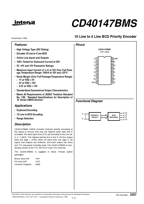
Functional Diagram
Applications
• Keyboard Encoding • 10 Line to BCD Encoding • Range Selection
3. For accuracy, voltage is measured differentially to VDD. Limit is 0.050V max.
9 0 PRIORITY SELECT BCD ENCODER D C B A 23 22 21 20
Description
CD40147BMS CMOS encoder features priority encoding of the inputs to ensure that only the highest order data line is encoded. Ten data input lines (0-9) are encoded to four line (8, 4, 2, 1) BCD. The highest priority line is line 9. All four output lines are logic 1 (VSS) when all input lines are logic 0. All inputs and outputs are buffered, and each output can drive one TTL low power Schottky load. The CD40147BMS is functionally similar to the TTL 54/74147 if pin 15 is tied low. The CD40147BMS is supplied in these 16-lead outline packages: Braze Seal DIP Frit Seal DIP Ceramic Flatpack H4T H1E H6W
CD4000系列芯片功能

CD4000系列芯片功能CD4000系列芯片功能型号器件名称备注CD4000 双3输入端或非门+单非门 TICD4001 四2输入端或非门 HIT/NSC/TI/GOLCD4002 双4输入端或非门 NSCCD4006 18位串入/串出移位寄存器 NSCCD4007 双互补对加反相器 NSCCD4008 4位超前进位全加器 NSCCD4009 六反相缓冲/变换器 NSCCD4010 六同相缓冲/变换器 NSCCD4011 四2输入端与非门 HIT/TICD4012 双4输入端与非门 NSCCD4013 双主-从D型触发器 FSC/NSC/TOSCD4014 8位串入/并入-串出移位寄存器 NSCCD4015 双4位串入/并出移位寄存器 TICD4016 四传输门 FSC/TICD4017 十进制计数/分配器 FSC/TI/MOTCD4018 可预制1/N计数器 NSC/MOTCD4019 四与或选择器 PHICD4020 14级串行二进制计数/分频器 FSCCD4021 08位串入/并入-串出移位寄存器PHI/NSC CD4022 八进制计数/分配器 NSC/MOTCD4023 三3输入端与非门 NSC/MOT/TICD4024 7级二进制串行计数/分频器 NSC/MOT/TICD4025 三3输入端或非门 NSC/MOT/TICD4026 十进制计数/7段译码器 NSC/MOT/TICD4027 双J-K触发器 NSC/MOT/TICD4028 BCD码十进制译码器 NSC/MOT/TICD4029 可预置可逆计数器 NSC/MOT/TICD4030 四异或门 NSC/MOT/TI/GOLCD4031 64位串入/串出移位存储器 NSC/MOT/TICD4032 三串行加法器 NSC/TICD4033 十进制计数/7段译码器 NSC/TICD4034 8位通用总线寄存器 NSC/MOT/TICD4035 4位并入/串入-并出/串出移位寄存NSC/MOT/TI CD4038 三串行加法器 NSC/TICD4040 12级二进制串行计数/分频器 NSC/MOT/TICD4041 四同相/反相缓冲器 NSC/MOT/TICD4042 四锁存D型触发器 NSC/MOT/TICD4043 4三态R-S锁存触发器("1"触发) NSC/MOT/TI CD4044 四三态R-S锁存触发器("0"触发) NSC/MOT/TI CD4046 锁相环NSC/MOT/TI/PHICD4047 无稳态/单稳态多谐振荡器 NSC/MOT/TICD4048 4输入端可扩展多功能门 NSC/HIT/TICD4049 六反相缓冲/变换器 NSC/HIT/TICD4050 六同相缓冲/变换器 NSC/MOT/TICD4051 八选一模拟开关 NSC/MOT/TICD4052 双4选1模拟开关 NSC/MOT/TICD4053 三组二路模拟开关 NSC/MOT/TICD4054 液晶显示驱动器 NSC/HIT/TICD4055 BCD-7段译码/液晶驱动器 NSC/HIT/TICD4056 液晶显示驱动器 NSC/HIT/TICD4059 “N”分频计数器 NSC/TICD4060 14级二进制串行计数/分频器 NSC/TI/MOTCD4063 四位数字比较器 NSC/HIT/TICD4066 四传输门 NSC/TI/MOTCD4067 16选1模拟开关 NSC/TICD4068 八输入端与非门/与门 NSC/HIT/TICD4069 六反相器 NSC/HIT/TICD4070 四异或门 NSC/HIT/TICD4071 四2输入端或门 NSC/TICD4072 双4输入端或门 NSC/TICD4073 三3输入端与门 NSC/TICD4075 三3输入端或门 NSC/TICD4076 四D寄存器CD4077 四2输入端异或非门 HITCD4078 8输入端或非门/或门CD4081 四2输入端与门 NSC/HIT/TICD4082 双4输入端与门 NSC/HIT/TICD4085 双2路2输入端与或非门CD4086 四2输入端可扩展与或非门CD4089 二进制比例乘法器CD4093 四2输入端施密特触发器 NSC/MOT/ST CD4094 8位移位存储总线寄存器 NSC/TI/PHI CD4095 3输入端J-K触发器CD4096 3输入端J-K触发器CD4097 双路八选一模拟开关CD4098 双单稳态触发器 NSC/MOT/TICD4099 8位可寻址锁存器 NSC/MOT/STCD40100 32位左/右移位寄存器CD40101 9位奇偶较验器CD40102 8位可预置同步BCD减法计数器CD40103 8位可预置同步二进制减法计数器CD40104 4位双向移位寄存器CD40105 先入先出FI-FD寄存器CD40106 六施密特触发器 NSC\TICD40107 双2输入端与非缓冲/驱动器 HAR\TICD40108 4字×4位多通道寄存器CD40109 四低-高电平位移器CD40110 十进制加/减,计数,锁存,译码驱动 STCD40147 10-4线编码器 NSC\MOTCD40160 可预置BCD加计数器 NSC\MOTCD40161 可预置4位二进制加计数器 NSC\MOTCD40162 BCD加法计数器 NSC\MOTCD40163 4位二进制同步计数器 NSC\MOTCD40174 六锁存D型触发器 NSC\TI\MOTCD40175 四D型触发器 NSC\TI\MOTCD40181 4位算术逻辑单元/函数发生器CD40182 超前位发生器CD40192 可预置BCD加/减计数器(双时钟) NSC\TICD40193 可预置4位二进制加/减计数器 NSC\TICD40194 4位并入/串入-并出/串出移位寄存NSC\MOT CD40195 4位并入/串入-并出/串出移位寄存NSC\MOT CD40208 4×4多端口寄存器。
CD4000系列说明

CD40xx,这个“xx”有很多,CD系列门电路CD4000 双3输入端或非门CD4001 四2输入端或非门CD4002 双4输入端或非门CD4007 双互补对加反向器CD4009 六反向缓冲/变换器CD4011 四2输入端与非门CD4012 双4输入端与非门CD4023 三2输入端与非门CD4025 三2输入端与非门CD4030 四2输入端异或门CD4041 四同相/反向缓冲器CD4048 8输入端可扩展多功能门CD4049 六反相缓冲/变换器CD4050 六同相缓冲/变换器CD4068 8输入端与门/与非门CD4069 六反相器CD4070 四2输入异或门CD4071 四2输入端或门CD4072 双4输入端或门CD4073 三3输入端与门CD4075 三3输入端或门CD4077 四异或非门CD4078 8输入端与非门/或门CD4081 四2输入端与门CD4082 双4输入端与非门CD4085 双2路2输入端与或非门CD4086 四2输入端可扩展与或非门CD40104 TTL至高电平CMOS转换器 CD40106 六施密特触发器CD40107 双2输入端与非缓冲/驱动器 CD40109 四低-高电平位移器CD4501 三多输入门CD4052 六反向缓冲器(三态输出)CD4503 六同相缓冲器(三态输出)CD4504 6TTL或CMOS同级移相器CD4506 双可扩展AIO门CD4507 四异或门CD4519 4位与/或选择器CD4530 双5输入多数逻辑门CD4572 四反向器加二输入或非门加二输入与非门CD4599 8位可寻址锁存器***************************************************触发器CD4013 双D触发器CD4027 双JK触发器CD4042 四锁存D型触发器CD4043 四三态R-S锁存触发器(“1”触发)CD4044 四三态R-S锁存触发器(“0”触发)CD4047 单稳态触发/无稳多谐振荡器CD4093 四2输入端施密特触发器CD4098 双单稳态触发器CD4099 8位可寻址锁存器CD4508 双4位锁存触发器CD4528 双单稳态触发器(与CD4098管脚相同,只是3、13脚复位开关为高电平有效) CD4538 精密单稳多谐振荡器CD4583 双施密特触发器CD4584 六施密特触发器CD4599 8位可寻址锁存器***************************************************计数器CD4017 十进制计数/分配器CD4020 14位二进制串行计数器/分频器CD4022 八进制计数/分配器CD4024 7位二进制串行计数器/分频器CD4029 可预置数可逆计数器(4位二进制或BCD码)CD4040 12二进制串行计数器/分频器CD4045 12位计数/缓冲器CD4059 四十进制N分频器CD4060 14二进制串行计数器/分频器和振荡器CD4095 3输入端J-K触发器(相同J-K输入端)CD4096 3输入端J-K触发器(相反和相同J-K输入端)CD40110 十进制加/减计数/锁存/7端译码/驱动器CD40160 可预置数BCD加计数器(异步复位)CD40161 可预置数4位二进制加计数器(R非=0时,CP上脉冲复位)(异步复位)CD40162 可预置数BCD加计数器(同步复位)CD40163 可预置数4位二进制加计数器(R非=0时,CP上脉冲复位)(同步复位)CD40192 可预置数BCD加/减计数器CD40193 可预置数4位二进制加/减计数器CD4510 可预置BCD加/减计数器CD4516 可预置4位二进制加/减计数器CD4518 双BCD同步加计数器CD4520 双同步4位二进制加计数器CD4521 24级频率分频器CD4522 可预置数BCD同步1/N加计数器CD4526 可预置数4位二进制同步1/N加计数器CD4534 实时与译码计数器CD4536 可编程定时器CD4541 可编程定时器CD4553 3数字BCD计数器CD4568 相位比较器/可编程计数器CD4569 双可预置BCD/二进制计数器CD4597 8位总线相容计数/锁存器CD4598 8位总线相容可建地址锁存器***************************************************译码器CD4511 BCD锁存/7段译码器/驱动器CD4514 4位锁存/4-16线译码器CD4515 4位锁存/4-16线译码器(负逻辑输出)CD4026 十进制计数/7段译码器(适用于时钟计时电路,利用C端的功能可方便的实现60或12分频)CD4028 BCD-十进制译码器CD4033 十进制计数/7段译码器CD4054 4位液晶显示驱动CD4055 BCD-7段码/液晶驱动CD4056 BCD-7段码/驱动CD40102 8位可预置同步减法计时器(BCD)CD40103 8位可预置同步减法计时器(二进制)CD4513 BCD-锁存/7端译码/驱动器(无效“0”不显)CD4514 4位锁存/4线—16线译码器(输出“1”)CD4515 4位锁存/4线—16线译码器(输出“0”)CD4543 BCD-锁存/7段译码/驱动器CD4544 BCD-锁存/7段译码/驱动器——波动闭锁CD4547 BCD-锁存/7段译码/大电流驱动器CD4555 双二进制4选1译码器/分离器(输出“1”)CD4556 双二进制4选1译码器/分离器(输出“0”)CD4558 BCD-7段译码CD4555 双二进制4选1译码器/分离器CD4556 双二进制4选1译码器/分离器(负逻辑输出)***************************************************移位寄存器CD4006 18位串入—串出移位寄存器CD4014 8位串入/并入—串出移位寄存器CD4015 双4位串入—并出移位寄存器CD4021 8位串入/并入—串出移位寄存器CD4031 64位移位寄存器CD4034 8位通用总线寄存器CD4035 4位串入/并入—串出/并出移位寄存器CD4076 4线D型寄存器CD4094 8位移位/存储总线寄存器CD40100 32位左移/右移CD40105 先进先出寄存器CD40108 4×4多端口寄存器阵列CD40194 4位并入/串入—并出/串出移位寄存器(左移/右移) CD40195 4位并入/串入—并出/串出移位寄存器CD4517 64位移位寄存器CD45490 连续的近似值寄存器CD4562 128位静态移位寄存器CD4580 4×4多端寄存器***************************************************模拟开关和数据选择器CD4016 四联双向开关CD4019 四与或选择器【Qn=(An*Ka)+(Bn*Kb)】CD4051 单八路模拟开关CD4052 双4路模拟开关CD4053 三2路模拟开关CD4066 四双向模拟开关CD4067 单十六路模拟开关CD4097 双八路模拟开关CD40257 四2选1数据选择器CD4512 八路数据选择器CD4529 双四路/单八路模拟开关CD4539 双四路数据选择器CD4551 四2通道模拟多路传输***************************************************运算电路CD4008 4位超前进位全加器CD4019 四与或选择器【Qn=(An*Ka)+(Bn*Kb)】CD4527 BCD比例乘法器CD4032 三路串联加法器CD4038 三路串联加法器(负逻辑)CD4063 四位量级比较器CD4070 四2输入异或门CD4585 4位数值比较器CD4089 4位二进制比例乘法器CD40101 9位奇偶发生器/校验器CD4527 BCD比例乘法器CD4531 12位奇偶数CD4559 逐次近似值码器CD4560 “N”BCD加法器CD4561 “9”求补器CD4581 4位算术逻辑单元CD4582 超前进位发生器CD4585 4位数值比较器***************************************************存储器CD4049 4字×8位随机存取存储器CD4505 64×1位RAMCD4537 256×1静态随机存取存储器CD4552 256位RAM***************************************************特殊电路CD4046 锁相环集成电路CD4532 8位优先编码器CD4500 工业控制单元CD4566 工业时基发生器CD4573 可预置运算放大器CD4574 比较器、线性、双对双运放CD4575 双/双预置运放/比较器CD4597 8位总线相容计数/锁存器CD4598 8位总线相容可建地址锁存器用带有置1端和置0端的触发器,如74HCT74、CD4013(D触发器),CD4027(JK触发器),还有计数器和译码器等。
IC芯片功能速查手册全

CD40106BCN FSC 六施密特触发器DATA
CD40107BE TI 双2 输入端与非缓冲/驱动器
CD40108 4 字×4 位多通道寄存器
CD40109BE TI 四低-高电平位移器
HCF40110BE ST 十进制加/减,计数,锁存,译码驱动
CD40181 4 位算术逻辑单元/函数发生器
CD40182 超前位发生器
CD40192BCN FSC 可预置BCD 加/减计数器(双时钟) DATA
CD40193BCN FSC 可预置4 位二进制加/减计ห้องสมุดไป่ตู้器DATA
CD40194 4 位并入/串入-并出/串出移位寄存
CD40195 4 位并入/串入-并出/串出移位寄存
CD4515BCN FSC 4 位锁存,4 线-16 线译码器DATA
CD4516 可预置4 位二进制加/减计数器
CD4517 双64 位静态移位寄存器
CD4518BE TI 双BCD 同步加计数器
HEF4518BP PHI 双BCD 同步加计数器
CD4519 四位与或选择器
HEF4520BP PHI 双4 位二进制同步加计数器
CD4053BE TI 三组二路模拟开关DATA
CD4054BE TI 液晶显示驱动器DATA
CD4055BE TI BCD-7 段译码/液晶驱动器DATA
CD4056BCN FSC 液晶显示驱动器DATA
HCF4058BE ST
CD4059BCN FSC “N”分频计数器DATA
CD4584 六施密特触发器
CD4585 4 位数值比较器
CD4049UBMJ中文资料
TL F 5971CD4049UBM CD4049UBC Hex Inverting Buffer CD4050BM CD4050BC Hex Non-Inverting BufferMarch 1988CD4049UBM CD4049UBC Hex Inverting Buffer CD4050BM CD4050BC Hex Non-Inverting BufferGeneral DescriptionThese hex buffers are monolithic complementary MOS (CMOS)integrated circuits constructed with N-and P-chan-nel enhancement mode transistors These devices feature logic level conversion using only one supply voltage (V DD ) The input signal high level (V IH )can exceed the V DD supply voltage when these devices are used for logic level conver-sions These devices are intended for use as hex buffers CMOS to DTL TTL converters or as CMOS current drivers and at V DD e 5 0V they can drive directly two DTL TTL loads over the full operating temperature rangeFeaturesY Wide supply voltage range 3 0V to 15V YDirect drive to 2TTL loads at 5 0V over full tempera-ture rangeY High source and sink current capabilityYSpecial input protection permits input voltages greater than V DDApplicationsY CMOS hex inverter bufferY CMOS to DTL TTL hex converterY CMOS current ‘‘sink’’or ‘‘source’’driver YCMOS high-to-low logic level converterConnection DiagramsCD4049UBM CD4049UBC Dual-In-Line PackageTL F 5971–1Top ViewOrder Number CD4049UB or CD4049BCD4050BM CD4050BC Dual-In-Line PackageTL F 5971–2Top ViewOrder Number CD4050UB or CD4050BC 1995National Semiconductor Corporation RRD-B30M105 Printed in U S AAbsolute Maximum Ratings(Notes1 2) If Military Aerospace specified devices are required please contact the National Semiconductor Sales Office Distributors for availability and specifications Supply Voltage(V DD)b0 5V to a18V Input Voltage(V IN)b0 5V to a18V Voltage at Any Output Pin(V OUT)b0 5V to V DD a0 5V Storage Temperature Range(T S)b65 C to a150 C Power Dissipation(P D)Dual-In-Line700mW Small Outline500mW Lead Temperature(T L)(Soldering 10seconds)260 C Recommended Operating Conditions(Note2)Supply Voltage(V DD)3V to15V Input Voltage(V IN)0V to15V Voltage at Any Output Pin(V OUT)0to V DD Operating Temperature Range(T A)CD4049UBM CD4050BM b55 C to a125 C CD4049UBC CD4050BC b40 C to a85 CDC Electrical Characteristics CD4049M CD4050BM(Note2)Symbol Parameter Conditionsb55 C a25 C a125 CUnits Min Max Min Typ Max Min MaxI DD Quiescent Device Current V DD e5V1 00 011 030m AV DD e10V2 00 012 060m AV DD e15V4 00 034 0120m A V OL Low Level Output Voltage V IH e V DD V IL e0Vl I O l k1m AV DD e5V0 0500 050 05VV DD e10V0 0500 050 05VV DD e15V0 0500 050 05V V OH High Level Output Voltage V IH e V DD V IL e0Vl I O l k1m AV DD e5V4 954 9554 95VV DD e10V9 959 95109 95VV DD e15V14 9514 951514 95V V IL Low Level Input Voltage l I O l k1m A(CD4050BM Only)V DD e5V V O e0 5V1 52 251 51 5VV DD e10V V O e1V3 04 53 03 0VV DD e15V V O e1 5V4 06 754 04 0V V IL Low Level Input Voltage l I O l k1m A(CD4049UBM Only)V DD e5V V O e4 5V1 01 51 01 0VV DD e10V V O e9V2 02 52 02 0VV DD e15V V O e13 5V3 03 53 03 0V V IH High Level Input Voltage l I O l k1m A(CD4050BM Only)V DD e5V V O e4 5V3 53 52 753 5VV DD e10V V O e9V7 07 05 57 0VV DD e15V V O e13 5V11 011 08 2511 0V V IH High Level Input Voltage l I O l k1m A(CD4049UBM Only)V DD e5V V O e0 5V4 04 03 54 0VV DD e10V V O e1V8 08 07 58 0VV DD e15V V O e1 5V12 012 011 512 0V I OL Low Level Output Current V IH e V DD V IL e0V(Note3)V DD e5V V O e0 4V5 64 653 2mAV DD e10V V O e0 5V129 8126 8mAV DD e15V V O e1 5V35294020mA Note1 ‘‘Absolute Maximum Ratings’’are those values beyond which the safety of the device cannot be guaranteed they are not meant to imply that the devices should be operated at these limits The table of‘‘Recommended Operating Conditions’’and‘‘Electrical Characteristics’’provides conditions for actual device operationNote2 V SS e0V unless otherwise specifiedNote3 These are peak output current capabilities Continuous output current is rated at12mA maximum The output current should not be allowed to exceed this value for extended periods of time I OL and I OH are tested one output at a time2DC Electrical Characteristics CD4049M CD4050BM(Note2)(Continued)Symbol Parameter Conditionsb55 C a25 C a125 CUnits Min Max Min Typ Max Min MaxI OH High Level Output Current V IH e V DD V IL e0V(Note3)V DD e5V V O e4 6V b1 3b1 1b1 6b0 72mAV DD e10V V O e9 5V b2 6b2 2b3 6b1 5mAV DD e15V V O e13 5V b8 0b7 2b12b5 0mAI IN Input Current V DD e15V V IN e0V b0 1b10b5b0 1b1 0m AV DD e15V V IN e15V0 110b50 11 0m A Note1 ‘‘Absolute Maximum Ratings’’are those values beyond which the safety of the device cannot be guaranteed they are not meant to imply that the devices should be operated at these limits The table of‘‘Recommended Operating Conditions’’and‘‘Electrical Characteristics’’provides conditions for actual device operationNote2 V SS e0V unless otherwise specifiedNote3 These are peak output current capabilities Continuous output current is rated at12mA maximum The output current should not be allowed to exceed this value for extended periods of time I OL and I OH are tested one output at a timeDC Electrical Characteristics CD4049UBC CD4050BC(Note2)Symbol Parameter Conditionsb40 C a25 C a85 CUnits Min Max Min Typ Max Min MaxI DD Quiescent Device Current V DD e5V40 034 030m AV DD e10V80 058 060m AV DD e15V160 0716 0120m A V OL Low Level Output Voltage V IH e V DD V IL e0Vl I O l k1m AV DD e5V0 0500 050 05VV DD e10V0 0500 050 05VV DD e15V0 0500 050 05V V OH High Level Output Voltage V IH e V DD V IL e0Vl I O l k1m AV DD e5V4 954 9554 95VV DD e10V9 959 95109 95VV DD e15V14 9514 951514 95V V IL Low Level Input Voltage l I O l k1m A(CD4050BC Only)V DD e5V V O e0 5V1 52 251 51 5VV DD e10V V O e1V3 04 53 03 0VV DD e15V V O e1 5V4 06 754 04 0V V IL Low Level Input Voltage l I O l k1m A(CD4049UBC Only)V DD e5V V O e4 5V1 01 51 01 0VV DD e10V V O e9V2 02 52 02 0VV DD e15V V O e13 5V3 03 53 03 0V V IH High Level Input Voltage l I O l k1m A(CD4050BC Only)V DD e5V V O e4 5V3 53 52 753 5VV DD e10V V O e9V7 07 05 57 0VV DD e15V V O e13 5V11 011 08 2511 0V V IH High Level Input Voltage l I O l k1m A(CD4049UBC Only)V DD e5V V O e0 5V4 04 03 54 0VV DD e10V V O e1V8 08 07 58 0VV DD e15V V O e1 5V12 012 011 512 0V Note1 ‘‘Absolute Maximum Ratings’’are those values beyond which the safety of the device cannot be guaranteed they are not meant to imply that the devices should be operated at these limits The table of‘‘Recommended Operating Conditions’’and‘‘Electrical Characteristics’’provides conditions for actual device operationNote2 V SS e0V unless otherwise specifiedNote3 These are peak output current capabilities Continuous output current is rated at12mA maximum The output current should not be allowed to exceed this value for extended periods of time I OL and I OH are tested one output at a time3DC Electrical Characteristics CD4049UBC CD4050BC(Note2)(Continued)Symbol Parameter Conditionsb40 C a25 C a85 CUnits Min Max Min Typ Max Min MaxI OL Low Level Output Current V IH e V DD V IL e0V(Note3)V DD e5V V O e0 4V4 64 053 2mAV DD e10V V O e0 5V9 88 5126 8mAV DD e15V V O e1 5V29254020mAI OH High Level Output Current V IH e V DD V IL e0V(Note3)V DD e5V V O e4 6V b1 0b0 9b1 6b0 72mAV DD e10V V O e9 5V b2 1b1 9b3 6b1 5mAV DD e15V V O e13 5V b7 1b6 2b12b5mAI IN Input Current V DD e15V V IN e0V b0 3b0 3b10b5b1 0m AV DD e15V V IN e15V0 30 310b51 0m A AC Electrical Characteristics CD4049UBM CD4049UBCT A e25 C C L e50pF R L e200k t r e t f e20ns unless otherwise specifiedSymbol Parameter Conditions Min Typ Max Unitst PHL Propagation Delay Time V DD e5V3065ns High-to-Low Level V DD e10V2040nsV DD e15V1530nst PLH Propagation Delay Time V DD e5V4585ns Low-to-High Level V DD e10V2545nsV DD e15V2035nst THL Transition Time V DD e5V3060ns High-to-Low Level V DD e10V2040nsV DD e15V1530nst TLH Transition Time V DD e5V60120ns Low-to-High Level V DD e10V3055nsV DD e15V2545nsC IN Input Capacitance Any Input1522 5pFAC Parameters are guaranteed by DC correlated testingAC Electrical Characteristics CD4050BM CD4050BCT A e25 C C L e50pF R L e200k t r e t f e20ns unless otherwise specifiedSymbol Parameter Conditions Min Typ Max Unitst PHL Propagation Delay Time V DD e5V60110ns High-to-Low Level V DD e10V2555nsV DD e15V2030nst PLH Propagation Delay Time V DD e5V60120ns Low-to-High Level V DD e10V3055nsV DD e15V2545nst THL Transition Time V DD e5V3060ns High-to-Low Level V DD e10V2040nsV DD e15V1530nst TLH Transition Time V DD e5V60120ns Low-to-High Level V DD e10V3055nsV DD e15V2545nsC IN Input Capacitance Any Input57 5pFAC Parameters are guaranteed by DC correlated testing4Schematic DiagramsCD4049UBM CD4049UBC1of6Identical UnitsTL F 5971–3CD4050BM CD4050BC1of6Identical UnitsTL F 5971–4 Switching Time WaveformsTL F 5971–5Typical ApplicationsCMOS to TTL or CMOS at a Lower V DDTL F 5971–6Note V DD1t V DD2Note In the case of the CD4049UBM CD4049UBCthe output drive capability increases with increasinginput voltage E g If V DD1e10V the CD4049UBMCD4049UBC could drive4TTL loads5C D 4049U B M C D 4049U B C H e x I n v e r t i n g B u f f e r C D 4050B M C D 4050B C H e x N o n -I n v e r t i n g B u f f e rPhysical Dimensions inches (millimeters)Ceramic Dual-In-Line Package (J)Order Number CD4049UBMJ CD4049UBCJ CD4049BMJ or CD4049BCJNS Package Number J16AMolded Dual-In-Line Package (N)Order Number CD4050BMN CD4050BCN CD4050BMN or CD4050BCNNS Package Number N16ELIFE SUPPORT POLICYNATIONAL’S PRODUCTS ARE NOT AUTHORIZED FOR USE AS CRITICAL COMPONENTS IN LIFE SUPPORT DEVICES OR SYSTEMS WITHOUT THE EXPRESS WRITTEN APPROVAL OF THE PRESIDENT OF NATIONAL SEMICONDUCTOR CORPORATION As used herein 1 Life support devices or systems are devices or 2 A critical component is any component of a life systems which (a)are intended for surgical implant support device or system whose failure to perform can into the body or (b)support or sustain life and whose be reasonably expected to cause the failure of the life failure to perform when properly used in accordance support device or system or to affect its safety or with instructions for use provided in the labeling can effectivenessbe reasonably expected to result in a significant injury to the userNational Semiconductor National Semiconductor National Semiconductor National Semiconductor CorporationEuropeHong Kong LtdJapan Ltd1111West Bardin RoadFax (a 49)0-180-530858613th Floor Straight Block Tel 81-043-299-2309。
CD4054中文资料
Data sheet acquired from Harris Semiconductor SCHS048IMPORTANT NOTICETexas Instruments and its subsidiaries (TI) reserve the right to make changes to their products or to discontinue any product or service without notice, and advise customers to obtain the latest version of relevant information to verify, before placing orders, that information being relied on is current and complete. All products are sold subject to the terms and conditions of sale supplied at the time of order acknowledgement, including those pertaining to warranty, patent infringement, and limitation of liability.TI warrants performance of its semiconductor products to the specifications applicable at the time of sale in accordance with TI’s standard warranty. Testing and other quality control techniques are utilized to the extent TI deems necessary to support this warranty. Specific testing of all parameters of each device is not necessarily performed, except those mandated by government requirements.CERTAIN APPLICATIONS USING SEMICONDUCTOR PRODUCTS MAY INVOLVE POTENTIAL RISKS OF DEATH, PERSONAL INJURY, OR SEVERE PROPERTY OR ENVIRONMENTAL DAMAGE (“CRITICAL APPLICATIONS”). TI SEMICONDUCTOR PRODUCTS ARE NOT DESIGNED, AUTHORIZED, OR WARRANTED TO BE SUITABLE FOR USE IN LIFE-SUPPORT DEVICES OR SYSTEMS OR OTHER CRITICAL APPLICATIONS. INCLUSION OF TI PRODUCTS IN SUCH APPLICATIONS IS UNDERSTOOD TO BE FULLY AT THE CUSTOMER’S RISK.In order to minimize risks associated with the customer’s applications, adequate design and operating safeguards must be provided by the customer to minimize inherent or procedural hazards.TI assumes no liability for applications assistance or customer product design. TI does not warrant or represent that any license, either express or implied, is granted under any patent right, copyright, mask work right, or other intellectual property right of TI covering or relating to any combination, machine, or process in which such semiconductor products or services might be or are used. TI’s publication of information regarding any third party’s products or services does not constitute TI’s approval, warranty or endorsement thereof.Copyright © 1999, Texas Instruments Incorporated。
CD440 CD445 手机快速入门指南说明书
Quick start guide
1 Connect 2 Install 3 Enjoy
philips
What’s in the box
CD440 Base station OR
CD440/CD445 Handset
CD445 Base Station
Power supply unit for base station
Rename your handset
1. Press to access the main menu 2. Press / to select PERSONAL SET 3. Press and / to select HANDSET NAME 4. Press to enter the handset name 5. Press to save the settings
<Group C>) 7. Press to save the entry
Access the phonebook
1. Press to access the phonebook 2. Press / to select your desired phonebook entry 3. Press to view the details of your selected phonebook entry
Need help?
User Manual See the User Manual that came with your CD440 or CD445.
Online help /support
7. Press to delete the current message
See CD445 user manual for details about the answering machine function.
CD4044BCSJX中文资料
© 2002 Fairchild Semiconductor Corporation DS005967October 1987Revised March 2002CD4043BC • CD4044BC Quad 3-STATE NOR R/S Latches • Quad 3-STATE NAND R/S LatchesCD4043BC • CD4044BCQuad 3-STATE NOR R/S Latches • Quad 3-STATE NAND R/S LatchesGeneral DescriptionThe CD4043BC are quad cross-couple 3-STATE CMOS NOR latches, and the CD4044BC are quad cross-couple 3-STATE CMOS NAND latches. Each latch has a separate Q output and individual SET and RESET inputs. There is a common 3-STATE ENABLE input for all four latches. A logic “1” on the ENABLE input connects the latch states to the Q outputs. A logic “0” on the ENABLE input discon-nects the latch states from the Q outputs resulting in an open circuit condition on the Q output. The 3-STATE fea-ture allows common bussing of the outputs.Featuress Wide supply voltage range: 3V to 15V s Low power:100 nW (typ.)s High noise immunity:0.45 V DD (typ.)s Separate SET and RESET inputs for each latch s NOR and NAND configurations 3-STATE output with common output enableApplications•Multiple bus storage •Strobed register•Four bits of independent storage with output enable •General digital logicOrdering Code:Devices also available in T ape and Reel. Specify by appending the suffix letter “X ” to the ordering code.Connection DiagramsPin Assignments for DIP , SOIC and SOPCD4043BCTop View Pin Assignments for DIP and SOICCD4044BCTop ViewOrder Number Package NumberPackage DescriptionCD4043BCM M16A 16-Lead Small Outline Integrated Circuit (SOIC), JEDEC MS-012, 0.150" Narrow CD4043BCN N16E 16-Lead Plastic Dual-In-Line Package (PDIP), JEDEC MS-001, 0.300" Wide CD4044BCM M16A 16-Lead Small Outline Integrated Circuit (SOIC), JEDEC MS-012, 0.150" Narrow CD4044BCSJ M16D 16-Lead Small Outline Package (SOP), EIAJ TYPE II, 5.3mm Wide CD4044BCNN16E16-Lead Plastic Dual-In-Line Package (PDIP), JEDEC MS-001, 0.300" Wide 2C D 4043B C • C D 4044B CBlock DiagramsCD4043BCCD4044BCTruth TablesCD4043BCCD4044BC OC = 3-STATE NC = No change X = Don ’t care∆ = Dominated by S = 1 input ∆∆ = Dominated by R = 0 inputS R E Q X X 0OC 001NC 10110110111∆S R E Q X X 0OC 111NC 011110101∆∆CD4043BC • CD4044BCAbsolute Maximum Ratings (Note 1)(Note 2)Recommended Operating Conditions (Note 2)Note 1: “Absolute Maximum Ratings ” are those values beyond which the safety of the device cannot be guaranteed; they are not meant to imply that the devices should be operated at these limits. The tables of “Recom-mended Operating Conditions ” and “Electrical Characteristics ” provide con-ditions for actual device operation.Note 2: V SS = 0V unless otherwise specified.DC Electrical Characteristics (Note 2)Note 3: I OH and I OL are tested one output at a time.Supply Voltage (V DD )−0.5V to +18V Input Voltage (V IN )−0.5V to V DD +0.5V Storage Temperature Range (T S )−65°C to +150°CPower Dissipation (P D )Dual-In-Line 700 mW Small Outline 500 mWLead Temperature (T L )(Soldering, 10 seconds)260°C Supply Voltage (V DD ) 3.0V to 15V Input Voltage (V IN )0 to V DD VOperating Temperature Range (T A )CD4043BC, CD4044BC−55°C to +125°CSymbol ParameterConditions−55°C +25°C +125°C UnitsMinMax MinTyp Max MinMax I DDQuiescent V DD = 5V, V IN = V DD or V SS 50.015150µADevice CurrentV DD = 10V, V IN = V DD or V SS 100.0110300V DD = 15V, V IN = V DD or V SS 200.0220600V OLLOW Level |I O | ≤ 1 µA, V IL = 0V, V IH = V DD Output VoltageV DD = 5.0V 0.0500.050.05VV DD = 10V 0.0500.050.05V DD = 15V0.0500.050.05V OHHIGH Level |I O | ≤ 1 µA, V IL = 0V, V IH = V DD Output VoltageV DD = 5.0V 4.95 4.95 5.0 4.95VV DD = 10V 9.959.95109.95V DD = 15V14.9514.951514.95V ILLOW Level |I O | ≤ 1 µAInput VoltageV DD = 5.0V, V O = 0.5V or 4.5V 1.5 2.25 1.5 1.5VV DD = 10V, V O = 1.0V or 9.0V 3.0 4.5 3.0 3.0V DD = 15V, V O = 1.5V or 13.5V4.06.75 4.0 4.0V IHHIGH Level |I O | ≤ 1 µAInput VoltageV DD = 5.0V, V O = 0.5V or 4.5V 3.5 3.5 2.75 3.5VV DD = 5.0V, V O = 1.0V or 9.0V 7.07.0 5.57.0V DD = 15V, V O = 1.5V or 13.5V11118.2511I OLLOW Level V IL = 0V, V IH = V DD Output Current V DD = 5.0V, V O = 0.4V 0.640.51 1.00.36mA(Note 3)V DD = 10V, V O = 0.5V 1.6 1.3 2.60.9V DD = 15V, V O = 1.5V 4.2 3.4 6.8 2.4I OHHIGH Level V IL = 0V, V IH = V DD Output Current V DD = 5.0V, V O = 4.6V −0.64−0.51−0.4−0.36mA(Note 3)V DD = 10V, V O = 9.5V −1.6−1.3−1.0−0.9V DD = 15V, V O = 13.5V −4.2−3.4−3.0−2.4I INInput CurrentV DD = 15V, V IN = 0V −0.1−10.5−0.1−1.0µAV DD = 15V, V IN = 15V0.110.50.1 1.0 4C D 4043B C • C D 4044B CAC Electrical Characteristics (Note 4)T A = 25°C, C L = 50 pF, R L = 200k, input t r = t f = 20 ns, unless otherwise notedNote 4: AC Parameters are guaranteed by DC correlated testing.Timing WaveformsCD4043BCD4044BEnable TimingSymbol ParameterConditions Min Typ Max Units t PLH , t PHLPropagation Delay S or R to QV DD = 5.0V 175350nsV DD = 10V 75175V DD = 15V60120t PZH , t PHZPropagation Delay Enable to Q (HIGH)V DD = 5.0V 115230nsV DD = 10V 55110V DD = 15V4080t PZL , t PLZPropagation Delay Enable to Q (LOW)V DD = 5.0V 100200nsV DD = 10V 50100V DD = 15V4080t THL , t TLHTransition TimeV DD = 5.0V 100200nsV DD = 10V 50100V DD = 15V4080t WOMinimum SET or RESET Pulse WidthV DD = 5.0V 80160ns V DD = 10V 4080V DD = 15V2040C INInput Capacitance5.07.5pFCD4043BC • CD4044BCPhysical Dimensionsinches (millimeters) unless otherwise noted16-Lead Small Outline Integrated Circuit (SOIC), JEDEC MS-012, 0.150" NarrowPackage Number M16A 6C D 4043B C • C D 4044B CPhysical Dimensionsinches (millimeters) unless otherwise noted (Continued)16-Lead Small Outline Package (SOP), EIAJ TYPE II, 5.3mm WidePackage Number M16D7CD4043BC • CD4044BC Quad 3-STATE NOR R/S Latches • Quad 3-STATE NAND R/S LatchesPhysical Dimensions inches (millimeters) unless otherwise noted (Continued)16-Lead Plastic Dual-In-Line Package (PDIP), JEDEC MS-001, 0.300" WidePackage Number N16EFairchild does not assume any responsibility for use of any circuitry described, no circuit patent licenses are implied and Fairchild reserves the right at any time without notice to change said circuitry and specifications.LIFE SUPPORT POLICYFAIRCHILD ’S PRODUCTS ARE NOT AUTHORIZED FOR USE AS CRITICAL COMPONENTS IN LIFE SUPPORT DEVICES OR SYSTEMS WITHOUT THE EXPRESS WRITTEN APPROVAL OF THE PRESIDENT OF FAIRCHILD SEMICONDUCTOR CORPORATION. As used herein:1.Life support devices or systems are devices or systems which, (a) are intended for surgical implant into the body, or (b) support or sustain life, and (c) whose failure to perform when properly used in accordance with instructions for use provided in the labeling, can be rea-sonably expected to result in a significant injury to the user.2. A critical component in any component of a life support device or system whose failure to perform can be rea-sonably expected to cause the failure of the life support device or system, or to affect its safety or effectiveness.。
CD4049 手册
TL F 5971CD4049UBM CD4049UBC Hex Inverting Buffer CD4050BM CD4050BC Hex Non-Inverting BufferMarch 1988CD4049UBM CD4049UBC Hex Inverting Buffer CD4050BM CD4050BC Hex Non-Inverting BufferGeneral DescriptionThese hex buffers are monolithic complementary MOS (CMOS)integrated circuits constructed with N-and P-chan-nel enhancement mode transistors These devices feature logic level conversion using only one supply voltage (V DD ) The input signal high level (V IH )can exceed the V DD supply voltage when these devices are used for logic level conver-sions These devices are intended for use as hex buffers CMOS to DTL TTL converters or as CMOS current drivers and at V DD e 5 0V they can drive directly two DTL TTL loads over the full operating temperature rangeFeaturesY Wide supply voltage range 3 0V to 15V YDirect drive to 2TTL loads at 5 0V over full tempera-ture rangeY High source and sink current capabilityYSpecial input protection permits input voltages greater than V DDApplicationsY CMOS hex inverter bufferY CMOS to DTL TTL hex converterY CMOS current ‘‘sink’’or ‘‘source’’driver YCMOS high-to-low logic level converterConnection DiagramsCD4049UBM CD4049UBC Dual-In-Line PackageTL F 5971–1Top ViewOrder Number CD4049UB or CD4049BCD4050BM CD4050BC Dual-In-Line PackageTL F 5971–2Top ViewOrder Number CD4050UB or CD4050BC 1995National Semiconductor Corporation RRD-B30M105 Printed in U S AAbsolute Maximum Ratings(Notes1 2) If Military Aerospace specified devices are required please contact the National Semiconductor Sales Office Distributors for availability and specifications Supply Voltage(V DD)b0 5V to a18V Input Voltage(V IN)b0 5V to a18V Voltage at Any Output Pin(V OUT)b0 5V to V DD a0 5V Storage Temperature Range(T S)b65 C to a150 C Power Dissipation(P D)Dual-In-Line700mW Small Outline500mW Lead Temperature(T L)(Soldering 10seconds)260 C Recommended Operating Conditions(Note2)Supply Voltage(V DD)3V to15V Input Voltage(V IN)0V to15V Voltage at Any Output Pin(V OUT)0to V DD Operating Temperature Range(T A)CD4049UBM CD4050BM b55 C to a125 C CD4049UBC CD4050BC b40 C to a85 CDC Electrical Characteristics CD4049M CD4050BM(Note2)Symbol Parameter Conditionsb55 C a25 C a125 CUnits Min Max Min Typ Max Min MaxI DD Quiescent Device Current V DD e5V1 00 011 030m AV DD e10V2 00 012 060m AV DD e15V4 00 034 0120m A V OL Low Level Output Voltage V IH e V DD V IL e0Vl I O l k1m AV DD e5V0 0500 050 05VV DD e10V0 0500 050 05VV DD e15V0 0500 050 05V V OH High Level Output Voltage V IH e V DD V IL e0Vl I O l k1m AV DD e5V4 954 9554 95VV DD e10V9 959 95109 95VV DD e15V14 9514 951514 95V V IL Low Level Input Voltage l I O l k1m A(CD4050BM Only)V DD e5V V O e0 5V1 52 251 51 5VV DD e10V V O e1V3 04 53 03 0VV DD e15V V O e1 5V4 06 754 04 0V V IL Low Level Input Voltage l I O l k1m A(CD4049UBM Only)V DD e5V V O e4 5V1 01 51 01 0VV DD e10V V O e9V2 02 52 02 0VV DD e15V V O e13 5V3 03 53 03 0V V IH High Level Input Voltage l I O l k1m A(CD4050BM Only)V DD e5V V O e4 5V3 53 52 753 5VV DD e10V V O e9V7 07 05 57 0VV DD e15V V O e13 5V11 011 08 2511 0V V IH High Level Input Voltage l I O l k1m A(CD4049UBM Only)V DD e5V V O e0 5V4 04 03 54 0VV DD e10V V O e1V8 08 07 58 0VV DD e15V V O e1 5V12 012 011 512 0V I OL Low Level Output Current V IH e V DD V IL e0V(Note3)V DD e5V V O e0 4V5 64 653 2mAV DD e10V V O e0 5V129 8126 8mAV DD e15V V O e1 5V35294020mA Note1 ‘‘Absolute Maximum Ratings’’are those values beyond which the safety of the device cannot be guaranteed they are not meant to imply that the devices should be operated at these limits The table of‘‘Recommended Operating Conditions’’and‘‘Electrical Characteristics’’provides conditions for actual device operationNote2 V SS e0V unless otherwise specifiedNote3 These are peak output current capabilities Continuous output current is rated at12mA maximum The output current should not be allowed to exceed this value for extended periods of time I OL and I OH are tested one output at a time2DC Electrical Characteristics CD4049M CD4050BM(Note2)(Continued)Symbol Parameter Conditionsb55 C a25 C a125 CUnits Min Max Min Typ Max Min MaxI OH High Level Output Current V IH e V DD V IL e0V(Note3)V DD e5V V O e4 6V b1 3b1 1b1 6b0 72mAV DD e10V V O e9 5V b2 6b2 2b3 6b1 5mAV DD e15V V O e13 5V b8 0b7 2b12b5 0mAI IN Input Current V DD e15V V IN e0V b0 1b10b5b0 1b1 0m AV DD e15V V IN e15V0 110b50 11 0m A Note1 ‘‘Absolute Maximum Ratings’’are those values beyond which the safety of the device cannot be guaranteed they are not meant to imply that the devices should be operated at these limits The table of‘‘Recommended Operating Conditions’’and‘‘Electrical Characteristics’’provides conditions for actual device operationNote2 V SS e0V unless otherwise specifiedNote3 These are peak output current capabilities Continuous output current is rated at12mA maximum The output current should not be allowed to exceed this value for extended periods of time I OL and I OH are tested one output at a timeDC Electrical Characteristics CD4049UBC CD4050BC(Note2)Symbol Parameter Conditionsb40 C a25 C a85 CUnits Min Max Min Typ Max Min MaxI DD Quiescent Device Current V DD e5V40 034 030m AV DD e10V80 058 060m AV DD e15V160 0716 0120m A V OL Low Level Output Voltage V IH e V DD V IL e0Vl I O l k1m AV DD e5V0 0500 050 05VV DD e10V0 0500 050 05VV DD e15V0 0500 050 05V V OH High Level Output Voltage V IH e V DD V IL e0Vl I O l k1m AV DD e5V4 954 9554 95VV DD e10V9 959 95109 95VV DD e15V14 9514 951514 95V V IL Low Level Input Voltage l I O l k1m A(CD4050BC Only)V DD e5V V O e0 5V1 52 251 51 5VV DD e10V V O e1V3 04 53 03 0VV DD e15V V O e1 5V4 06 754 04 0V V IL Low Level Input Voltage l I O l k1m A(CD4049UBC Only)V DD e5V V O e4 5V1 01 51 01 0VV DD e10V V O e9V2 02 52 02 0VV DD e15V V O e13 5V3 03 53 03 0V V IH High Level Input Voltage l I O l k1m A(CD4050BC Only)V DD e5V V O e4 5V3 53 52 753 5VV DD e10V V O e9V7 07 05 57 0VV DD e15V V O e13 5V11 011 08 2511 0V V IH High Level Input Voltage l I O l k1m A(CD4049UBC Only)V DD e5V V O e0 5V4 04 03 54 0VV DD e10V V O e1V8 08 07 58 0VV DD e15V V O e1 5V12 012 011 512 0V Note1 ‘‘Absolute Maximum Ratings’’are those values beyond which the safety of the device cannot be guaranteed they are not meant to imply that the devices should be operated at these limits The table of‘‘Recommended Operating Conditions’’and‘‘Electrical Characteristics’’provides conditions for actual device operationNote2 V SS e0V unless otherwise specifiedNote3 These are peak output current capabilities Continuous output current is rated at12mA maximum The output current should not be allowed to exceed this value for extended periods of time I OL and I OH are tested one output at a time3DC Electrical Characteristics CD4049UBC CD4050BC(Note2)(Continued)Symbol Parameter Conditionsb40 C a25 C a85 CUnits Min Max Min Typ Max Min MaxI OL Low Level Output Current V IH e V DD V IL e0V(Note3)V DD e5V V O e0 4V4 64 053 2mAV DD e10V V O e0 5V9 88 5126 8mAV DD e15V V O e1 5V29254020mAI OH High Level Output Current V IH e V DD V IL e0V(Note3)V DD e5V V O e4 6V b1 0b0 9b1 6b0 72mAV DD e10V V O e9 5V b2 1b1 9b3 6b1 5mAV DD e15V V O e13 5V b7 1b6 2b12b5mAI IN Input Current V DD e15V V IN e0V b0 3b0 3b10b5b1 0m AV DD e15V V IN e15V0 30 310b51 0m A AC Electrical Characteristics CD4049UBM CD4049UBCT A e25 C C L e50pF R L e200k t r e t f e20ns unless otherwise specifiedSymbol Parameter Conditions Min Typ Max Unitst PHL Propagation Delay Time V DD e5V3065ns High-to-Low Level V DD e10V2040nsV DD e15V1530nst PLH Propagation Delay Time V DD e5V4585ns Low-to-High Level V DD e10V2545nsV DD e15V2035nst THL Transition Time V DD e5V3060ns High-to-Low Level V DD e10V2040nsV DD e15V1530nst TLH Transition Time V DD e5V60120ns Low-to-High Level V DD e10V3055nsV DD e15V2545nsC IN Input Capacitance Any Input1522 5pFAC Parameters are guaranteed by DC correlated testingAC Electrical Characteristics CD4050BM CD4050BCT A e25 C C L e50pF R L e200k t r e t f e20ns unless otherwise specifiedSymbol Parameter Conditions Min Typ Max Unitst PHL Propagation Delay Time V DD e5V60110ns High-to-Low Level V DD e10V2555nsV DD e15V2030nst PLH Propagation Delay Time V DD e5V60120ns Low-to-High Level V DD e10V3055nsV DD e15V2545nst THL Transition Time V DD e5V3060ns High-to-Low Level V DD e10V2040nsV DD e15V1530nst TLH Transition Time V DD e5V60120ns Low-to-High Level V DD e10V3055nsV DD e15V2545nsC IN Input Capacitance Any Input57 5pFAC Parameters are guaranteed by DC correlated testing4Schematic DiagramsCD4049UBM CD4049UBC1of6Identical UnitsTL F 5971–3CD4050BM CD4050BC1of6Identical UnitsTL F 5971–4 Switching Time WaveformsTL F 5971–5Typical ApplicationsCMOS to TTL or CMOS at a Lower V DDTL F 5971–6Note V DD1t V DD2Note In the case of the CD4049UBM CD4049UBCthe output drive capability increases with increasinginput voltage E g If V DD1e10V the CD4049UBMCD4049UBC could drive4TTL loads5C D 4049U B M C D 4049U B C H e x I n v e r t i n g B u f f e r C D 4050B M C D 4050B C H e x N o n -I n v e r t i n g B u f f e rPhysical Dimensions inches (millimeters)Ceramic Dual-In-Line Package (J)Order Number CD4049UBMJ CD4049UBCJ CD4049BMJ or CD4049BCJNS Package Number J16AMolded Dual-In-Line Package (N)Order Number CD4050BMN CD4050BCN CD4050BMN or CD4050BCNNS Package Number N16ELIFE SUPPORT POLICYNATIONAL’S PRODUCTS ARE NOT AUTHORIZED FOR USE AS CRITICAL COMPONENTS IN LIFE SUPPORT DEVICES OR SYSTEMS WITHOUT THE EXPRESS WRITTEN APPROVAL OF THE PRESIDENT OF NATIONAL SEMICONDUCTOR CORPORATION As used herein 1 Life support devices or systems are devices or 2 A critical component is any component of a life systems which (a)are intended for surgical implant support device or system whose failure to perform can into the body or (b)support or sustain life and whose be reasonably expected to cause the failure of the life failure to perform when properly used in accordance support device or system or to affect its safety or with instructions for use provided in the labeling can effectivenessbe reasonably expected to result in a significant injury to the userNational Semiconductor National Semiconductor National Semiconductor National Semiconductor CorporationEuropeHong Kong LtdJapan Ltd1111West Bardin RoadFax (a 49)0-180-530858613th Floor Straight Block Tel 81-043-299-2309。
- 1、下载文档前请自行甄别文档内容的完整性,平台不提供额外的编辑、内容补充、找答案等附加服务。
- 2、"仅部分预览"的文档,不可在线预览部分如存在完整性等问题,可反馈申请退款(可完整预览的文档不适用该条件!)。
- 3、如文档侵犯您的权益,请联系客服反馈,我们会尽快为您处理(人工客服工作时间:9:00-18:30)。
Data sheet acquired from Harris Semiconductor SCHS041D − Revised October 2003The CD4043B and CD4044B types are supplied in 16-lead hermetic dual-in-line ceramic packages (F3A suffix), 16-lead dual-in-line plastic packages (E suffix), 16-lead small-outline packages (D, DR, DT, DW, DWR, and NSR suffixes), and 16-lead thin shrink small-outline packages (PW and PWR suffixes).PACKAGING INFORMATIONOrderable Device Status(1)PackageType PackageDrawingPins PackageQtyEco Plan(2)Lead/Ball Finish MSL Peak Temp(3)CD4043BD ACTIVE SOIC D1640Pb-Free(RoHS)CU NIPDAU Level-2-260C-1YEAR/Level-1-235C-UNLIMCD4043BDR ACTIVE SOIC D162500Pb-Free(RoHS)CU NIPDAU Level-2-260C-1YEAR/Level-1-235C-UNLIMCD4043BDT ACTIVE SOIC D16250Pb-Free(RoHS)CU NIPDAU Level-2-260C-1YEAR/Level-1-235C-UNLIMCD4043BDW ACTIVE SOIC DW1640Pb-Free(RoHS)CU NIPDAU Level-2-250C-1YEAR/Level-1-235C-UNLIMCD4043BDWR ACTIVE SOIC DW162000Pb-Free(RoHS)CU NIPDAU Level-2-250C-1YEAR/Level-1-235C-UNLIMCD4043BE ACTIVE PDIP N1625Pb-Free(RoHS)CU NIPDAU Level-NC-NC-NC CD4043BF3A ACTIVE CDIP J161None Call TI Level-NC-NC-NC CD4043BM OBSOLETE SOIC D16None Call TI Call TICD4043BNSR ACTIVE SO NS162000Pb-Free(RoHS)CU NIPDAU Level-2-260C-1YEAR/Level-1-235C-UNLIMCD4043BPW ACTIVE TSSOP PW1690Pb-Free(RoHS)CU NIPDAU Level-1-250C-UNLIMCD4043BPWR ACTIVE TSSOP PW162000Pb-Free(RoHS)CU NIPDAU Level-1-250C-UNLIMCD4044BD ACTIVE SOIC D1640Pb-Free(RoHS)CU NIPDAU Level-2-260C-1YEAR/Level-1-235C-UNLIMCD4044BDR ACTIVE SOIC D162500Pb-Free(RoHS)CU NIPDAU Level-2-260C-1YEAR/Level-1-235C-UNLIMCD4044BDT ACTIVE SOIC D16250Pb-Free(RoHS)CU NIPDAU Level-2-260C-1YEAR/Level-1-235C-UNLIMCD4044BDW ACTIVE SOIC DW1640Pb-Free(RoHS)CU NIPDAU Level-2-250C-1YEAR/Level-1-235C-UNLIMCD4044BDWR ACTIVE SOIC DW162000Pb-Free(RoHS)CU NIPDAU Level-2-250C-1YEAR/Level-1-235C-UNLIMCD4044BE ACTIVE PDIP N1625Pb-Free(RoHS)CU NIPDAU Level-NC-NC-NC CD4044BF ACTIVE CDIP J161None Call TI Level-NC-NC-NC CD4044BF3A ACTIVE CDIP J161None Call TI Level-NC-NC-NC CD4044BM OBSOLETE SOIC D16None Call TI Call TICD4044BNSR ACTIVE SO NS162000Pb-Free(RoHS)CU NIPDAU Level-2-260C-1YEAR/Level-1-235C-UNLIMCD4044BPW ACTIVE TSSOP PW1690Pb-Free(RoHS)CU NIPDAU Level-1-250C-UNLIMCD4044BPWR ACTIVE TSSOP PW162000Pb-Free(RoHS)CU NIPDAU Level-1-250C-UNLIM(1)The marketing status values are defined as follows:ACTIVE:Product device recommended for new designs.LIFEBUY:TI has announced that the device will be discontinued,and a lifetime-buy period is in effect.NRND:Not recommended for new designs.Device is in production to support existing customers,but TI does not recommend using this part in a new design.PREVIEW:Device has been announced but is not in production.Samples may or may not be available.OBSOLETE:TI has discontinued the production of the device.(2)Eco Plan-May not be currently available-please check /productcontent for the latest availability information and additional product content details.None:Not yet available Lead(Pb-Free).Pb-Free(RoHS):TI's terms"Lead-Free"or"Pb-Free"mean semiconductor products that are compatible with the current RoHS requirements for all6substances,including the requirement that lead not exceed0.1%by weight in homogeneous materials.Where designed to be soldered at high temperatures,TI Pb-Free products are suitable for use in specified lead-free processes.Green(RoHS&no Sb/Br):TI defines"Green"to mean"Pb-Free"and in addition,uses package materials that do not contain halogens, including bromine(Br)or antimony(Sb)above0.1%of total product weight.(3)MSL,Peak Temp.--The Moisture Sensitivity Level rating according to the JEDECindustry standard classifications,and peak solder temperature.Important Information and Disclaimer:The information provided on this page represents TI's knowledge and belief as of the date that it is provided.TI bases its knowledge and belief on information provided by third parties,and makes no representation or warranty as to the accuracy of such information.Efforts are underway to better integrate information from third parties.TI has taken and continues to take reasonable steps to provide representative and accurate information but may not have conducted destructive testing or chemical analysis on incoming materials and chemicals.TI and TI suppliers consider certain information to be proprietary,and thus CAS numbers and other limited information may not be available for release.In no event shall TI's liability arising out of such information exceed the total purchase price of the TI part(s)at issue in this document sold by TI to Customer on an annual basis.IMPORTANT NOTICETexas Instruments Incorporated and its subsidiaries (TI) reserve the right to make corrections, modifications, enhancements, improvements, and other changes to its products and services at any time and to discontinue any product or service without notice. Customers should obtain the latest relevant information before placing orders and should verify that such information is current and complete. All products are sold subject to TI’s terms and conditions of sale supplied at the time of order acknowledgment.TI warrants performance of its hardware products to the specifications applicable at the time of sale in accordance with TI’s standard warranty. T esting and other quality control techniques are used to the extent TI deems necessary to support this warranty. Except where mandated by government requirements, testing of all parameters of each product is not necessarily performed.TI assumes no liability for applications assistance or customer product design. Customers are responsible for their products and applications using TI components. T o minimize the risks associated with customer products and applications, customers should provide adequate design and operating safeguards.TI does not warrant or represent that any license, either express or implied, is granted under any TI patent right, copyright, mask work right, or other TI intellectual property right relating to any combination, machine, or process in which TI products or services are used. Information published by TI regarding third-party products or services does not constitute a license from TI to use such products or services or a warranty or endorsement thereof. Use of such information may require a license from a third party under the patents or other intellectual property of the third party, or a license from TI under the patents or other intellectual property of TI.Reproduction of information in TI data books or data sheets is permissible only if reproduction is without alteration and is accompanied by all associated warranties, conditions, limitations, and notices. Reproduction of this information with alteration is an unfair and deceptive business practice. TI is not responsible or liable for such altered documentation.Resale of TI products or services with statements different from or beyond the parameters stated by TI for that product or service voids all express and any implied warranties for the associated TI product or service and is an unfair and deceptive business practice. TI is not responsible or liable for any such statements. Following are URLs where you can obtain information on other Texas Instruments products and application solutions:Products ApplicationsAmplifiers Audio /audioData Converters Automotive /automotiveDSP Broadband /broadbandInterface Digital Control /digitalcontrolLogic Military /militaryPower Mgmt Optical Networking /opticalnetwork Microcontrollers Security /securityTelephony /telephonyVideo & Imaging /videoWireless /wirelessMailing Address:Texas InstrumentsPost Office Box 655303 Dallas, Texas 75265Copyright 2005, Texas Instruments Incorporated。