TMS470R1A64数据手册
HPA-MCUINTERFACE;中文规格书,Datasheet资料

1IntroductionUser's GuideSLAU106–June 2005The HPA-MCU Interface Board was designed to provide a complete system develop-ment platform using evaluation modules from the Data Acquisition Products Group.This board passes control and data signals from a variety of Micro Controller and Digital Signal Processors (DSP)to and from A-to-D and D-to-A converter evaluation modules (EVM's)from Texas Instruments.DSP boards compatible with this interface card include theTMS320F2812eZdsp™platforms from Spectrum Digital MicroController boards compatible with this interface When combined with sensor or amplifier boards,the HPA-MCU Interface Board can provide a complete data acquisition system for a variety of applications.Contents1Introduction ..........................................................................................12Signal Conditioning Sites ..........................................................................33Serial Interface EVM Sites ........................................................................44Parallel Interface EVM Sites ......................................................................65Related Documentation From Texas Instruments . (86)HPA-MCU Interface Board Assembly and Board Schematics ................................9List of Tables1External Power Connections ......................................................................32Signal Conditioning I/O Connections .............................................................33Signal Conditioning Power Connections—JP1,JP2,JP3and JP4..........................44Typical F2812Serial Site Digital I/O Connections—J11and J12............................45Typical F2808Serial Site Digital I/O Connections—J11and J12............................56Serial Power Connections—JP5and JP6.......................................................57Analog I/O Connections—J6and J5.............................................................68Parallel Control Connections—J13...............................................................69Parallel Data Bus Connections—J14 (710)Bill of Materials ......................................................................................9The HPA-MCU Interface Board is intended to provide Data Converter customers with the greatest amount of flexibility for the evaluation of Data Acquisition Products from Texas Instruments.The HPA-MCU Interface the guidelines set forth in the Designing Modular EVM's for Data Acquisition Products document and provides access to the SCI,SPI,CAN and I2C ports found on the 2000well as the MSP430and TMS470micro controllers.The Multi Channel BufferedSerial Port (McBSP)of the TMS320F2812is also supported,as is the parallel data bus found on both the TMS320F2407and TMS320F2812.eZdsp is a trademark of Spectrum Digital.HPA-MCU Interface BoardSLAU106–June 200511.1DSP and Micro Controller Board Options1.2Communication Options1.3Power Connections to the InterfaceCardIntroductionThe interface board consists of two signal conditioning sites,two serial EVM sites and a parallel EVM site.Regardless of the interface type,all EVM's compatible with the HPA-MCU Interface Board have astandard analog interface and standard power connector.Three position screw terminals J1and J4and two position screw terminals J7,J8,J9,and J10provide access to a common power bus routed to all sites.The HPA-MCU board is supplied with male pin headers in connector locations J15,J16and J17.These male pin headers are intended to plug into female mating connectors installed on the bottom side of the user supplied micro controller or DSP board.J15serves the parallel address and data bus found on the TMS320F2407and TMS320F2812DSP.J16serves the McBSP port found on the TMS320F2812.J17serves General Purpose Input/Output (GPIO),SCI,SPI,CAN and I2C ports.Recomended mating connectors to J15,J16and J17are Samtec part numbers SSW-130-21-G-D,SSW-120-21-G-S and SSW-120-21-G-Dregarding the mating connectors can be obtained from the Samtec website at The TMS320F2407,TMS320F2808and TMS320F2812eZdsp™Development Systems from Spectrum Digital (sold as stand alone products)do not ship with the appropriate mating connectors installed.Spectrum Digital's warranty expressly states that any user modification made to their DevleopmentSystems are done so at the customers risk.Customer installed mating connectors may void the eZdsp™product warranty.Bundled Development Systems which include appropriate mating connectors as well as the HPA-MCU Interface Board may be available for purchase through Spectrum Digital.Please contact Spectrum Digital for additional information.The HPA-MCU board provides three 9-Pin sub D connectors for CAN and RS232communication options.J18and J19are DB9Female and DB9Male (respectivly)connectors.These two connectors areassociated with the SCI ports found on the TMS320and TMS470processors platforms.DPDT switchSW2is provided as a means to implement a "Null-Modem"connection between the serial ports in order to achieve loop back testing.When SW2is in the "normal"position,the TX and RX lines associated with SCI port 1are connected to J18pins 2and 3(respectively).When SW2is switched to the "null modem"position,the TX and RX connections of SCI port 1are swapped.TX is connected to J18pin 3and RX is connected to J18pin 2.The combination of male and female DB9connectors,as well as U7-a dual port MAX3232,allow the use of readily available standard 9-Pin serial cables to be used to test serial communication between J18and J19and ports 1/2of the installed processor.J20is associated with U10-an SN65HV2353.3V CAN transciever.Loop back communication options between two CAN ports may be available depending on the installed micro controller or DSP board.The SN65HV235can also provide an internal loopback function by closing jumper W2(default condition).The screw terminals along the bottom edge of the HPA-MCU Interface Board give access to the common power bus.Three port terminals J1and J4provide analog power.Two port terminals J7,J8,J9,and J10provide the digital voltages.Two resistor locations,R7and R8,located on the interface board give the user the option of powering the installed Micro Controller or DSP board through the Interface Board common power bus.HPA-MCU Interface Board SLAU106–June 200522Signal Conditioning Sites2.1Signal Conditioning I/O Connector Signal Conditioning SitesAnalog and digital power to compatible data converter EVM's must always be supplied from a clean,well regulated external source via J1,J4,and J7–J10.For best analog performance,linear power supplies are recommended.Table1shows the typical external power connections.Table1.External Power ConnectionsScrew Terminal Applied Voltage Typical FunctionJ1±VA(±15VMax)Analog Voltage–Provide analog power for signal conditioning,sensor boards,amplifiers,etc.J4±5V(±5.5VMax)Analog Voltage–Provide analog power for signal conditioning,sensor boards,amplifiers,etc.J7+5(5.5Max)Digital Voltage–Power to digital logic–ADC's,DAC's,etc.J8+VD(undefined)Digital Voltage–Reserved for future useJ9+1.8V(2.3VMax)Digital Voltage–Core logic voltage for CODEC's,etc.J10+3.3V(3.7VMax)Digital Voltage–Power to digital logic–ADC's,DAC's,etc.The signal conditioning sites provide a20pin analog I/O header,as well as a6-pin header for the analog power supply connections.A second20-pin header is provided for added stability of signal conditioning boards.The Analog I/O connectors,J2and J3,are designed to provide up to eight single ended or four differential channels to/from the data converter EVM's.External reference voltages may also be applied to the data converter through the analog I/O connector.Since the reference requirements vary by converter type,no restrictions are placed on the input voltage levels.Be sure to check the documentation for the EVM before applying any input signals.Single and dual channel converters will leave the unused pins open.Table2 shows the standard analog connector pin out.Table2.Signal Conditioning I/O ConnectionsSignal Pin Number SignalA0(–)12A0(+)A1(–)34A1(+)A2(–)56A2(+)A3(–)78A3(+)AGND910A4AGND1112A5AGND1314A6VCOM1516A7AGND1718REF–AGND1920REF+The20-pin headers located beside JP1and JP2provide stability for the signal conditioning boards–no signals are routed to or from these connectors.These connectors are labeled Analog1and Analog2on the interface board silk screen and in the assembly drawing found in Section6of this manual.HPA-MCU Interface BoardSLAU106–June200532.2Signal Conditioning Power Connector3Serial Interface EVM Sites3.1Serial Site Digital I/O ConnectionsSerial Interface EVM SitesThe Interface Board provides a common power bus to both signal conditioning sites.The power connector used on the Interface Board is a 6pin male header.Four power connectors JP1,JP2,JP3and JP4are provided—each with the same pin out.The purpose of this is to allow an A-to-D converter to use the same signal conditioning board as a D-to-A converter,simply by rotating the signal conditioning board 180additional details,please refer to the DAP Signal Conditioning Board Users Guide Table 3shows the power connector voltages supplied to the signal conditioning module.Table 3.Signal Conditioning Power Connec-tions—JP1,JP2,JP3and JP4Signal Pin NumberSignal +VA 12–VA +5VA 34–5VA AGND56AGNDThe serial interface consists of two serial digital I/O connectors (J11and J12),two power connectors (JP5and JP6)and two analog I/O connectors (J5and J6).The analog I/O connectors are configured as pass through connections from/to the signal conditioning site connectors J2and J3.The digital I/O connectors are 20pin male headers providing access to the various signals defined in the F2407,F2808and F2812eZdsp™.Reference Manuals,as well as the TMS470R1A1024Reference Manual.SPST switch SW1.1controls the signals available to Serial Site 2through a pair ofSN74CBTLV3257FET Muxes located at U6and U8.When SW1.1is open (silkscreen marked "0"),J11is normally connected to an Serial Peripheral Interface (SPI)port.When SW1.1is closed (silkscreen marked "1"),Serial Site 2may be used with the Multi channel Buffered Serial Port (McBSP)found on TMS320F2812DSP's.Table 4shows the serial connector pin out for the F2812eZdsp™.Table 4.Typical F2812Serial Site Digital I/O Connections—J11and J12SignalPin NumberSignal Site 1Site 2(J11)Site 2(J11)Site 1Site 2(J11)Site 2(J11)(J12)SW1.1Open SW1.1Closed(J12)SW1.1Open SW1.1ClosedNC CLKOUT IOPB912IOPA11IOPA7IOPA7SPICLKa PWM12MCLKXa 34DGND DGND DGND IOPA12CAP1/QEP1MCLKRa 56CANTXa CANTXa CANTXa SPISTEa T1PWM/T1CMMFSXa 78CANRXa CANRXa CANRXa P IOPB1CAP2/QEP2MFSRa 910DGND DGND DGND SPISIMOa PWM10MDXa 1112IOPA4IOPA5IOPA5SPISOMIa PWM11MDRa 1314IOPA3IOPA3IOPA3XINT1CAP3/QEPI1XINT21516IOPD5IOPD5IOPD5PWM1PWM2PWM21718DGND DGND DGND T1CTRIPXINT1IOPE01920IOPB8IOPB8IOPB8HPA-MCU Interface Board 4SLAU106–June 20053.2Serial Power Connector Serial Interface EVM SitesMost of the signals shown above can be configured as simple GPIO.In general,the TMS320F2812will support an SPI(clock stop)type interface as well as a McBSP(continuous clock)type interface.TheMcBSP port can also work in SPI mode,providing two identicle operating modes on J11and J12.With the exception of the McBSP signals,the F2407eZdsp™provides the same connections shown in Table4.Note:Several serial interface EVM's require the use of a GPIO signal applied to pin1of theirdigital I/O connector.When serial site1of the HPA-MCU Interface is used with the F2812in SPI mode,a two pin shunt jumper placed between pins1and2may be able tofacilitate the GPIO requirements.Please consult the schematic in the EVM users guide tosee if this is possible.The muxing of the peripherals on the TMS320F2808provide a slightly different interconnection scheme.The F2808device does not support McBSP protocol,so J11and J12are configured as two independent SPI ports.Table5shows the serial connector pin out for the F2808eZdsp™.Table5.Typical F2808Serial Site Digital I/O Connections—J11and J12Signal Pin Number SignalSite1Site2(J11)Site2(J11)Site1Site2(J11)Site2(J11)(J12)SW1.1Open SW1.1Closed(J12)SW1.1Open SW1.1ClosedGPIO7GPIO11NC12GPIO13GPIO6GPIO6SPICLKa SPICLKb NC34DGND DGND DGNDGPIO34GPIO6NC56CANTXa CANTXa CANTXaSPISTEa SPISTEb NC78CANRXa CANRXa CANRXaGPIO9GPIO21NC910DGND DGND DGNDSPISIMOa SPISIMOb NC1112GPIO5GPIO5GPIO5SPISOMIa SPISOMIb NC1314GPIO3GPIO3GPIO3GPIO14GPIO34GPIO231516SCLa SCLa SCLaEPWM1A GPIO1GPIO11718DGND DGND DGNDGPIO12GPIO15GPIO151920SDAa SDAa SDAa The Interface Board provides a common power bus to both serial sites.The power connector used on the Interface Board is a10pin male header.Two power connectors JP5and JP6are provided—each with the same pin out.JP5sevices serial Site2,while JP6services serial Site1.Table6shows the powerconnector voltages supplied to the signal conditioning module.Table6.Serial Power Connections—JP5and JP6Signal(1)Pin Number Signal+VA12–VA+5VA34–5VADGND56AGND+1.8VD78VD1+3.3VD910+5VD(1)P5is also used for the parallel EVM site.HPA-MCU Interface BoardSLAU106–June200553.3Analog I/O Connectors4Parallel Interface EVM Sites4.1Parallel Analog I/O and Power Connections4.2Parallel Control ConnectorParallel Interface EVM SitesAs mentioned previously,the analog I/O connectors act as pass through connectors to the signal conditioning sites.Table 7shows the analog signals passed to/from signal conditioning module to the input/output of compatible modular EVM's.Table 7.Analog I/O Connections—J6and J5Signal Pin NumberSignal A0(–)12A0(+)A1(–)34A1(+)A2(–)56A2(+)A3(–)78A3(+)AGND 910A4AGND 1112A5VCOM 1314A6AGND 1516A7AGND 1718REF–REFIN1920REF+The parallel interface consists of a 32-pin header (J14)which provides access up to 16parallel data bits,and a 20-pin parallel control header (J13).The parallel control header provides 4-muxed address lines,read and write strobes,interrupt capabilities,chip select and clock signals.Analog I/O and power is also provided.The parallel site uses the same analog I/O and power connections described in the serial interface section of this manual.Typically,a parallel ADC EVM will use the analog interface connector located at J6,and the power connector located at JP5.A parallel DAC EVM will typically use the analog connector located at J5.If pass through power connections are made on either the DAC or ADC EVM,the ADC and DAC boards could be stacked allowing a complete signal chain to be realized.Read the specific EVM Users Guide to determine if a stacking arrangement is possible.See the previous sections for pin out details of the analog I/O and power connectors.The parallel control connector feeds chip select,read,write and address lines to the parallel EVM's.The address decoding for most parallel EVM's will be done on the EVM card itself,lending way to thepossibility of stacking several cards together.Table 8shows the typical signals found on parallel interface EVM's,designed to be used with the HPA-MCU Interface Board.Table 8.Parallel Control Connections—J13SignalPin NumberSignal DC_CSa (DS,PS or IS via W3)12DGND WE 34DGND RE56DGND EVM_A0(A2or A12)78DGND EVM_A1(A3or A13)910DGND EVM_A2(A4or A14)1112DGNDHPA-MCU Interface Board SLAU106–June 200564.3Parallel Data Bus Connector Parallel Interface EVM SitesTable8.Parallel Control Connections—J13(continued)Signal Pin Number SignalEVM_A3(A5or A15)1314DGNDGPIO(SPARE–NC)1516DGNDT2PWM1718DGNDXINT21920DGNDDC_CSa is intended to act as a chip select to the EVM,not necessarily the actual data converter being evaluated.Carefully read the documentation that came with your EVM for details on how this signal isused.W3allows the user to connect the card to I/O,Data or Program space.The EVM address lines EVM_A0through EVM_A3are fed from a four bit2:1bus switch,U5.Typically, this provides access to DSP address lines A2..A5,or A12..A15.SPST switch SW1.2controls whichaddress lines are sent to the parallel control connector.When SW1.2is closed,address lines A12through A15are sent to the data converter EVM.When SW1.2is open,the EVM uses address lines A2through A5.The Parallel data connector used on the Interface Card is a32pin male header.Typical parallel EVM's will have a data bus that is a minimum of16bits wide and a maximum of24bits.The C2000Interface Board is limited to a16bit data bus,but accepts cards designed to the24-bit wide maximum.Data isaligned LSB to LSB.Table9shows the parallel data bus connections.Table9.Parallel Data Bus Connections—J14Signal Pin Number SignalD012DGNDD134DGNDD256DGNDD378DGNDD4910DGNDD51112DGNDD61314DGNDD71516DGNDD81718DGNDD91920DGNDD102122DGNDD112324DGNDD122526DGNDD132728DGNDD142930DGNDD153132DGNDHPA-MCU Interface BoardSLAU106–June200575Related Documentation From5.1Related Third Party Related Documentation From Texas Instruments1.Designing Modular EVM's for2.DAP Signal Conditioning Board3.MAX3232,Multichannel RS-2324.SN74CBTD3861,10-Bit Bus5.SN65HVD235,CAN Tranceiver6.SN74LVTH16245,16-Bit Bus7.SN74CBT3257,4-Bit 1-of-21.LF2407A eZdsp Technical 2.LF2808eZdsp Technical Reference 3.LF2812eZdsp Technical Reference HPA-MCU Interface Board 8SLAU106–June 2005HPA-MCU Interface Board Assembly and Board Schematics 6HPA-MCU Interface Board Assembly and Board SchematicsTable10shows the Bill of Materials(BOM)for the HPA-MCU Interface Board.Table10.Bill of MaterialsDesignators Description Manufacturer Mfg.Part NumberC1C2C3C5C6C70.1µF,0805,Ceramic,X7R,50V,10%TDK C2012X7R1E104KC8C10C13C14C15C16C17C18C19C20C4C9C11C1233µF,16V,Aluminum Panasonic ECEV1AA330SRANALOG1&2J2J310Pin,Dual Row,SMT Header(20Pos.)Samtec TSW-110-07-L-DJ5J6J11J12J13J1416Pin,Dual Row,SMT Header(32Pos.)Samtec TSW-116-07-L-DJP1JP2JP3JP4W13Pin,Dual Row,SMT Header(6Pos.)Samtec TSW-103-07-L-DJP5JP65Pin,Dual Row,SMT Header(10Pos.)Samtec TSW-105-07-L-DJ7J8J9J102Terminal Screw Commector OST ED1514J1J43Terminal Screw Commector OST ED1515J1530Pin,Dual Row,SMT Header(60Pos.)Samtec TSW-130-07-L-DJ1620Pin,Single Row,SMT Header(20Pos.)Samtec TSW-120-07-L-SJ1720Pin,Dual Row,SMT Header(40Pos.)Samtec TSW-120-07-L-DJ18J20DB9Female,Right Angle AMP/Tyco747844-4J19DB9Male,Right Angle AMP/Tyco747840-4L1L215µH Inductor,SMT,1608Series Inductors,Inc.CTDS1608C-153R1R2R3R5R610KΩ,0805,5%,0.1W resistor Yageo America9C08052A1002JLHFTR4R9120Ω,0805,5%,0.1W resistor Yageo America9C08052A1200JLHFTR7R8Not InstalledSW14Position SPST Switch CTS Corp218-10LPSTSW2DPDT Slide Switch E-Switch EG2209U1U2U1110-Bit FET Bus Switch With Level Shifting Texas Instruments SN74CBTD3861PWU3U416-Bit Bus Transciever Texas Instruments SN74LVTH16245ADGGRU5U6U8U94-Bit1of2FET Multiplexer/Demultiplexer Texas Instruments SN74CBTLV3257PWRU7Multichannel RS-232Line Driver/Reciever Texas Instruments MAX3232CPWRU10 3.3V Can Tranceiver with Auto Loop-back Texas Instruments SN65HVD235DW22Pin,TH Header Samtec TSW-102-07-L-SSLAU106–June20059HPA-MCU Interface Board分销商库存信息:TIHPA-MCUINTERFACE。
MOTEC α系列伺服使用手册v1.1
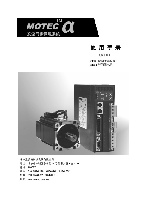
使用手册
(V1.0)
SED 型伺服驱动器 SEM 型伺服电机
北京意美德科技发展有限公司 地址: 北京市东城区东中街 58 号美惠大厦 B 座 703A 邮编: 100027 电话: 010-65542170、65546546、65542692 传真: 010-65546721 65547015 网址:
α系列伺服电机系统使用手册
章 节:
第 1 章. 伺服电机与驱动器型号 第 2 章. 安装和配线 第 3 章. 驱动器 JP2 接口(I/O 控制信号)功能说明 第 4 章. 面板操作操作说明 第 5 章. 性能调整功能说明 第 6 章. 控制模式 第 7 章. 监视项 第 8 章. 伺服驱动器工作时序图 第 9 章.驱动器 JP3/JP4(通信端口)定义、接线及通信协议 附录 1: 驱动器参数列表 附录 2:故障信息、故障原因及处理措施 附录 3:SEM 电机电气参数
1. 伺服电机与驱动器型号 ................................................................. 5 1.1 伺服电机型号定义 ................................................................. 5 1.2 伺服驱动器型号定义 ............................................................... 6 1.3 α系列驱动器与电机组合 ........................................................... 6 1.4 α系列驱动器外形及安装尺寸图 ..................................................... 8
德州仪器AM64x 嵌入式工控控制终端 SK-AM64 评估套件说明书

一块高端工业控制终端好选择 —— SK-AM64评估套件测评近几年嵌入式最火的领域,各种工控网关终端绝对算得上一个。
智能家电和工控设备更新换代,对控制终端提出了越来越多的要求,各老牌大厂都不断在更新自己的方案。
目前对这个领域的方案主要需求是更高的安全性、更高的集成度、更高的稳定性、更强的性能,但是开发者如何选择一款合适的方案并非易事。
德州仪器(TI)新推出的AM64X系列方案绝对是目前此领域非常不错的的代表,这次就由我带大家了解一下基于AM64x处理器的评估套件SK-AM64。
开箱视频一、开箱SK-AM64评估套件使用纸质外盒包装,包装盒正面印着产品型号,背面是评估板板载资源的列表和简单的使用说明。
打开盒子可以看到由防静电袋装着开发板。
AM64x 入门套件是一个完整测试和开发平台,适合用于加速原型设计。
套件包括:有线和无线连接、三个扩展头、多个引导选项和灵活的调试功能。
配有TI 的AM64x 处理器和优化的功能集,允许用户使用基于以太网的接口、USB 接口、有线串行接口以及2.4GHz 和5GHz 无线通信来创建商业和工业解决方案。
两个板载1Gbps 以太网端口用于有线连接,此外还有三个扩展头用于扩展板功能。
此套件采用标准串行协议(如UART、I²C 和SPI),可用作通信网关与多个其他器件进行连接。
该入门套件可通过在A53 内核上运行Linux 进行评估,从而可作为远程工业通信网络中的中央引擎,也适合用作可编程逻辑控制器或运动控制器。
额外的嵌入式仿真逻辑允许使用标准开发工具(例如TI 的Code Composer Studio™)进行仿真和调试。
特性•软件:TI Processor SDK Linux/RT Linux/RTOS内核、Yocto文件系统、包含Wi-Fi® 的开箱即用例程•处理:AM64x,含2 个Arm Cortex-A53、4 个Arm Cortex-R5F、1个可以做安全功能使用的M4F,2 个PRU_ICSSG•通过 WiLink™8 WL1837MOD 模块实现双频带Wi-Fi®、Bluetooth®/低功耗蓝牙 5.1;2 个1000/100Mbps RJ-45 以太网接口•连接:可通过micro-USB 连接1 个Type A USB 3.1 gen1(超高速)、板载XDS110 JTAG 仿真器和 3 个UART•扩展和原型设计:40 引脚Raspberry Pi (RPI4) HAT、PRU-ICSSG 实时I/O 和TI-MCU 头•存储: 2GB LPDDR4;SK 上的可引导接口:可移除uSD、USB、16MB OSPI、以太网、UART开发需要自配的硬件•USB-C 5V 3A 电源•USB SD 卡写入器•Micro-SD 卡(16GB 或更大)•用于UART 串行通信的USB Micro-B 电缆•以太网电缆(可选)二、硬件描述此评估板集成了丰富的扩展接口,并且都是目前最流行的扩展接口,比如集成了兼容Raspberry Pi的扩展接口,这将能适配目前Raspberry Pi种类丰富的第三方外设模块,这将简化原型设计的难度而且更具可玩性,让开发者快速验证自己的创意。
S417400A-60DR资料

IMPORTANT NOTICETexas Instruments and its subsidiaries (TI) reserve the right to make changes to their products or to discontinue any product or service without notice, and advise customers to obtain the latest version of relevant information to verify, before placing orders, that information being relied on is current and complete. All products are sold subject to the terms and conditions of sale supplied at the time of order acknowledgement, including those pertaining to warranty, patent infringement, and limitation of liability.TI warrants performance of its semiconductor products to the specifications applicable at the time of sale in accordance with TI’s standard warranty. Testing and other quality control techniques are utilized to the extent TI deems necessary to support this warranty. Specific testing of all parameters of each device is not necessarily performed, except those mandated by government requirements.CERTAIN APPLICATIONS USING SEMICONDUCTOR PRODUCTS MAY INVOLVE POTENTIAL RISKS OF DEATH, PERSONAL INJURY, OR SEVERE PROPERTY OR ENVIRONMENTAL DAMAGE (“CRITICAL APPLICATIONS”). TI SEMICONDUCTOR PRODUCTS ARE NOT DESIGNED, AUTHORIZED, OR WARRANTED TO BE SUITABLE FOR USE IN LIFE-SUPPORT DEVICES OR SYSTEMS OR OTHER CRITICAL APPLICATIONS. INCLUSION OF TI PRODUCTS IN SUCH APPLICATIONS IS UNDERSTOOD TO BE FULLY AT THE CUSTOMER’S RISK.In order to minimize risks associated with the customer’s applications, adequate design and operating safeguards must be provided by the customer to minimize inherent or procedural hazards.TI assumes no liability for applications assistance or customer product design. TI does not warrant or represent that any license, either express or implied, is granted under any patent right, copyright, mask work right, or other intellectual property right of TI covering or relating to any combination, machine, or process in which such semiconductor products or services might be or are used. TI’s publication of information regarding any third party’s products or services does not constitute TI’s approval, warranty or endorsement thereof.Copyright © 1998, Texas Instruments Incorporated。
AT4708~64多路温度测试仪用户手册说明书

Rev.A0AT4708~64多路温度测试仪@安柏®是常州安柏精密仪器有限公司的商标或注册商标。
常州安柏精密仪器有限公司Applent Instruments Ltd.江苏省常州市钟楼区宝龙国际61-3F电话:************* 销售服务电子邮件:*****************技术支持电子邮件:****************©2005-2018 Applent Instruments.声明根据国际版权法,未经常州安柏精密仪器有限公司(Applent Instruments Inc.)事先允许和书面同意,不得以任何形式复制本文内容。
安全信息为避免可能的电击和人身安全,请遵循以下指南进行操作。
免责声明用户在开始使用仪器前请仔细阅读以下安全信息,对于用户由于未遵守下列条款而造成的人身安全和财产损失,安柏仪器将不承担任何责任。
仪器接地为防止电击危险,请连接好电源地线。
不可在爆炸性气体环境使用仪器不可在易燃易爆气体、蒸汽或多灰尘的环境下使用仪器。
在此类环境使用任何电子设备,都是对人身安全的冒险。
不可打开仪器外壳非专业维护人员不可打开仪器外壳,以试图维修仪器。
仪器在关机后一段时间内仍存在未释放干净的电荷,这可能对人身造成电击危险。
不要使用工作异常的仪器如果仪器工作不正常,其危险不可预知,请断开电源线,不可再使用,也不要试图自行维修。
不要超出本说明书指定的方式使用仪器超出范围,仪器所提供的保护措施将失效。
警告:不要加超过350V的直流电压或超过200V的交流电压到测试端,否则会损坏仪器。
安全标志:设备由双重绝缘或加强绝缘保护废弃电气和电子设备(WEEE) 指令2002/96/EC切勿丢弃在垃圾桶内声明:!,$,#,安柏标志和文字是常州安柏精密仪器有限公司的商标或注册商标。
有限担保和责任范围常州安柏精密仪器有限公司(以下简称安柏)保证您购买的每一台仪器在质量和计量上都是完全合格的。
NSR641RF-D01和NSR642RF-D01分段备自投装置技术及使用说明书V3.11

第六章 装置使用说明 ................................................. 43 6.1 NSR600RF-D 系列装置显示操作说明 ................................. 43 6.2 显示菜单及操作使用说明 .......................................... 50
快,采样精度高; ü 测量精度系数单独存放在交流采样模件的 E2PROM 中,独立性好,便于维护; ü 保护定值多区域相对独立的 E2PROM/DSRAM 中存放,自动互相校验,自行修复,
投退保护压板,便于现场的运行; ü 交流量开关量录波功能、录波波形就地显示及后台软件分析相结合; ü 通讯可采用 CAN 网、485、光纤、以太网等介质,以单网、双网、三网方式
与监控系统通讯,通讯速度快、可靠性高,支持 IEC60870-5-103 标准; ü 32 位浮点功能的 DSP 和 16 位 AD 宽幅模数转换,24 点/周波采样,运算速度
NS2000 变电站综合自动化系统
NSR641RF-D01/NSR642RF-D01 分段备自投 装置
液晶电子工业有限公司产品数据手册:液晶电子电机启动器套件、联击器、热过载保护传感器说明书
T h e i n f o r m a t i o n p r o v i d e d i n t h i s d o c u m e n t a t i o n c o n t a i n s g e n e r a l d e s c r i p t i o n s a n d /o r t e c h n i c a l c h a r a c t e r i s t i c s o f t h e p e r f o r m a n c e o f t h e p r o d u c t s c o n t a i n e d h e r e i n .T h i s d o c u m e n t a t i o n i s n o t i n t e n d e d a s a s u b s t i t u t e f o r a n d i s n o t t o b e u s e d f o r d e t e r m i n i n g s u i t a b i l i t y o r r e l i a b i l i t y o f t h e s e p r o d u c t s f o r s p e c i f i c u s e r a p p l i c a t i o n s .I t i s t h e d u t y o f a n y s u c h u s e r o r i n t e g r a t o r t o p e r f o r m t h e a p p r o p r i a t e a n d c o m p l e t e r i s k a n a l y s i s , e v a l u a t i o n a n d t e s t i n g o f t h e p r o d u c t s w i t h r e s p e c t t o t h e r e l e v a n t s p e c i f i c a p p l i c a t i o n o r u s e t h e r e o f .N e i t h e r S c h n e i d e r E l e c t r i c I n d u s t r i e s S A S n o r a n y o f i t s a f f i l i a t e s o r s u b s i d i a r i e s s h a l l b e r e s p o n s i b l e o r l i a b l e f o r m i s u s e o f t h e i n f o r m a t i o n c o n t a i n e d h e r e i n .Product data sheetCharacteristicsLR9D32KITD18BDTESYS motor starter kit, LC1D18BD contactor,LR9D32 thermal overload relayProduct availability: Non-Stock - Not normally stocked in distribution facility MainRange TeSysProduct or componenttypeMotor starterContactor application Motor controlResistive loadUtilisation category AC-4AC-1AC-3Poles description3PPower pole contactcomposition3 NO[Ue] rated operationalvoltagePower circuit <= 690 V AC 25...400 HzPower circuit <= 300 V DC[Ie] rated operationalcurrent18 A 140 °F (60 °C)) <= 440 V AC AC-3 power cir-cuit32 A 140 °F (60 °C)) <= 440 V AC AC-1 power circuit Motor power kW4 KW 220...230 V AC 50/60 Hz AC-3)7.5 KW 380...400 V AC 50/60 Hz AC-3)9 KW 415...440 V AC 50/60 Hz AC-3)10 KW 500 V AC 50/60 Hz AC-3)10 KW 660...690 V AC 50/60 Hz AC-3)4 kW 400 V AC 50/60 Hz AC-4)Motor power HP (UL /CSA)1 Hp 115 V AC 50/60 Hz 1 phase3 Hp 230/240 V AC 50/60 Hz 1 phase5 Hp 200/208 V AC 50/60 Hz 3 phase5 Hp 230/240 V AC 50/60 Hz 3 phase10 Hp 460/480 V AC 50/60 Hz 3 phase15 hp 575/600 V AC 50/60 Hz 3 phaseControl circuit type DC standard[Uc] control circuit volt-age24 V DCAuxiliary contact com-position1 NO + 1 NC[Uimp] rated impulsewithstand voltage6 kV IEC 60947Overvoltage category III[Ith] conventional freeair thermal current10 A 140 °F (60 °C) signalling circuit32 A 140 °F (60 °C) power circuitIrms rated making ca-pacity140 A AC signalling circuit IEC 60947-5-1250 A DC signalling circuit IEC 60947-5-1300 A 440 V power circuit IEC 60947Rated breaking capacity300 A 440 V power circuit IEC 60947[Icw] rated short-timewithstand current145 A 104 °F (40 °C) - 10 s power circuit240 A 104 °F (40 °C) - 1 s power circuit40 A 104 °F (40 °C) - 10 min power circuit84 A 104 °F (40 °C) - 1 min power circuit100 A - 1 s signalling circuit120 A - 500 ms signalling circuit140 A - 100 ms signalling circuitAssociated fuse rating10 A gG signalling circuit IEC 60947-5-150 A gG <= 690 V type 1 power circuit35 A gG <= 690 V type 2 power circuitAverage impedance 2.5 mOhm - Ith 32 A 50 Hz power circuit[Ui] rated insulation volt-agePower circuit 690 V IEC 60947-4-1Power circuit 600 V CSAPower circuit 600 V ULSignalling circuit 690 V IEC 60947-1Signalling circuit 600 V CSASignalling circuit 600 V ULElectrical durability 1.65 Mcycles 18 A AC-3 <= 440 V1 Mcycles 32 A AC-1 <= 440 VPower dissipation perpole2.5 W AC-10.8 W AC-3Safety cover WithMounting support PlateRailStandards CSA C22.2 No 14EN 60947-4-1EN 60947-5-1IEC 60947-4-1IEC 60947-5-1UL 508Product certifications LROS (Lloyds register of shipping)DNVGLRINABVCCCULCSAGOSTConnections - terminals Control circuit screw clamp terminals 1 0.00…0.01 in² (1…4 mm²)flexible without cable endControl circuit screw clamp terminals 2 0.00…0.01 in² (1…4 mm²)flexible without cable endControl circuit screw clamp terminals 1 0.00…0.01 in² (1…4 mm²)flexible with cable endControl circuit screw clamp terminals 2 0.00…0.00 in² (1…2.5 mm²)flexible with cable endControl circuit screw clamp terminals 1 0.00…0.01 in² (1…4 mm²)solid without cable endControl circuit screw clamp terminals 2 0.00…0.01 in² (1…4 mm²)solid without cable endPower circuit screw clamp terminals 1 0.00…0.01 in²(1.5…6 mm²)flexible without cable endPower circuit screw clamp terminals 2 0.00…0.01 in²(1.5…6 mm²)flexible without cable endPower circuit screw clamp terminals 1 0.00…0.01 in²(1…6 mm²)flexible with cable endPower circuit screw clamp terminals 2 0.00…0.01 in²(1…4 mm²)flexible with cable endPower circuit screw clamp terminals 1 0.00…0.01 in²(1.5…6 mm²)solid without cable endPower circuit screw clamp terminals 2 0.00…0.01 in²(1.5…6 mm²)solid without cable endTightening torque Power circuit 15.05 lbf.in (1.7 N.m) screw clamp ter-minals flat Ø 6 mmPower circuit 15.05 lbf.in (1.7 N.m) screw clamp ter-minals Philips No 2Control circuit 15.05 lbf.in (1.7 N.m) screw clampterminals flat Ø 6 mmControl circuit 15.05 lbf.in (1.7 N.m) screw clamp ter-minals Philips No 2Operating time53.55...72.45 ms closing16...24 ms openingSafety reliability level B10d = 1369863 cycles contactor with nominal loadEN/ISO 13849-1B10d = 20000000 cycles contactor with mechanicalload EN/ISO 13849-1Mechanical durability30 McyclesMaximum operating rate3600 cyc/h 140 °F (60 °C)Relay application Motor protectionPhase failure sensitivity Phase difference > 40% 3 s IEC 60947-4-1 ComplementaryCoil technology With integral suppression deviceControl circuit voltage limits Drop-out 0.1...0.25 Uc DC 140 °F (60 °C))Operational 0.7...1.25 Uc DC 140 °F (60 °C))Time constant28 msInrush power in W 5.4 W 68 °F (20 °C))Hold-in power consumption in W 5.4 W 68 °F (20 °C)Auxiliary contacts type Mechanically linked 1 NO + 1 NC IEC 60947-5-1Mirror contact 1 NC IEC 60947-4-1Signalling circuit frequency25...400 HzMinimum switching current5 mA signalling circuitMinimum switching voltage17 V signalling circuitNon-overlap time 1.5 Ms on de-energisation between NC and NO contact1.5 ms on energisation between NC and NO contactInsulation resistance> 10 MOhm signalling circuitContact compatibility M4Motor power range4…6 KW 200…240 V 3 phase7…11 KW 380…440 V 3 phase7…11 kW 480…500 V 3 phaseMotor starter type Direct on-line contactorContactor coil voltage24 V DC standardThermal overload class Class 5 (30)Thermal protection adjustment range 6.4…32 AMaximum power consumption in W300 mWMounting support Under contactorPlate, with specific accessoriesRail, with specific accessories[Ue] rated operational voltage690 V power circuit660 V signalling circuit[Ui] rated insulation voltage Power circuit 1000 VSignalling circuit 690 VTripping threshold 1.25 In IEC 60947-4-1Control type Red push-button stop and manual resetWhite 2 microswitches adjustable trip classRed knob automatic resetGrey dial full-load current adjustmentTime range 1.5...4 min - automatic reset time[Ith] conventional free air thermal current5 A signalling circuitAssociated fuse rating5 A gG signalling circuit5 A BS signalling circuit[Uimp] rated impulse withstand voltage6 kVIP degree of protection Front face IP20 IEC 60529Front face IP20 VDE 0106Mechanical robustness Vibrations 10...150 Hz 6 Gn) IEC 60068-2-6Shocks 11 ms 15 gn) IEC 60068-2-7Connections - terminals Control circuit screw clamp terminals 1 0.00 in² (2.5 mm²) solid or flexible - with-out cable endPower circuit screw clamp terminals 1 0.02 in² (16 mm²) solid or flexible - withoutcable endTightening torque Control circuit 0.8 N.m screw clamp terminalsPower circuit 3.1 N.m screw clamp terminalsEnvironmentIP degree of protection IP20 front face IEC 60529Protective treatment TH IEC 60068-2-30Pollution degree3Ambient air temperature for operation23…140 °F (-5…60 °C)-40…158 °F (-40…70 °C) at UcPermissible ambient air temperature around the de-viceOperating altitude9842.52 ft (3000 m) withoutMechanical robustness Vibrations contactor open2 Gn, 5...300 HzVibrations contactor closed4 Gn, 5...300 HzShocks contactor open10 Gn for 11 msShocks contactor closed15 Gn for 11 msHeight 3.03 in (77 mm)Width 1.77 in (45 mm)Depth 3.74 in (95 mm)Net weight 1.08 lb(US) (0.49 kg)Standards UL 60947-4-1IEC 60947-4-1CSA C22.2GB 14048.4Product certifications CSACCCTÜVCULusAmbient air temperature for operation-13…158 °F (-25…70 °C) IEC 60255-8Ambient air temperature for storage-76…176 °F (-60…80 °C)Ambient air temperature for storage-67…176 °F (-55…80 °C)Operating altitude6561.68 ft (2000 m) without deratingFire resistance1562 °F (850 °C) IEC 60695-2-1Flame retardance V1 UL 94Electromagnetic compatibility Surge withstand 2 kV common mode IEC 61000-4-5Resistance to electrostatic discharge 8 kV IEC 61000-4-2Immunity to radiated radio-electrical interference 10 V/m IEC 61000-4-3Immunity to fast transients 2 kV IEC 61000-4-4Dielectric strength6 kV 50 Hz IEC 60255-5Height 2.85 in (72.5 mm)Width 1.77 in (45 mm)Depth 3.15 in (79.9 mm)Net weight0.40 lb(US) (0.18 kg)Ordering and shipping detailsCategory22350 - LR9D AND TESYS D STARTER KITSDiscount Schedule I12Package weight(Lbs)0.80 kg (1.76 lb(US))Returnability YesCountry of origin CNOffer SustainabilityEU RoHS Directive Under investigation。
罗克韦尔自动化 信任 40 通道 120 Vdc 数字输入 FTA 用户手册说明书

PD-T8821 TrustedTrusted 40 Channel 120 Vdc Digital Input FTA Product OverviewThe Trusted® 40 Channel 120 Vdc Digital Input Field Termination Assembly (FTA) T8821 is designed to act as the main interface between a field device generating a digital signal and the Trusted TMR 120 Vdc Digital Input Module T8423.Features:•40 input channels per FTA.•Industry standard field device connections (2-wire).•Standard DIN rail compatibility.•Simple installation and connection.•120 Vdc operation.•SmartSlot connection for ‘one to many’ hot replacement of input modules.•Fused field power supply per channel.•On-board Light Emitting Diode (LED) indication of field power supply integrity.Trusted PD-T8821Page intentionally left blankPREFACEIn no event will Rockwell Automation be responsible or liable for indirect or consequential damages resulting from the use or application of this equipment. The examples given in this manual are included solely for illustrative purposes. Because of the many variables and requirements related to any particular installation, Rockwell Automation does not assume responsibility or reliability for actual use based on the examples and diagrams.No patent liability is assumed by Rockwell Automation, with respect to use of information, circuits, equipment, or software described in this manual.All trademarks are acknowledged.DISCLAIMERIt is not intended that the information in this publication covers every possible detail about the construction, operation, or maintenance of a control system installation. You should also refer to your own local (or supplied) system safety manual, installation and operator/maintenance manuals.REVISION AND UPDATING POLICYThis document is based on information available at the time of its publication. The document contents are subject to change from time to time. The latest versions of the manuals are available at the Rockwell Automation Literature Library under "Product Information" information "Critical Process Control & Safety Systems".TRUSTED RELEASEThis technical manual applies to Trusted Release: 3.6.1.LATEST PRODUCT INFORMATIONFor the latest information about this product review the Product Notifications and Technical Notes issued by technical support. Product Notifications and product support are available at the Rockwell Automation Support Centre atAt the Search Knowledgebase tab select the option "By Product" then scroll down and select the Trusted product.Some of the Answer ID’s in the Knowledge Base require a TechConnect Support Contract. For more information about TechConnect Support Contract Access Level and Features please click on the following link:https:///app/answers/detail/a_id/50871This will get you to the login page where you must enter your login details.IMPORTANT A login is required to access the link. If you do not have an account then you can create one using the "Sign Up" link at the top right of the web page.DOCUMENTATION FEEDBACKYour comments help us to write better user documentation. If you discover an error, or have a suggestion on how to make this publication better, send your comment to our technical support group at SCOPEThis manual specifies the maintenance requirements and describes the procedures to assist troubleshooting and maintenance of a Trusted system. WHO SHOULD USE THIS MANUALThis manual is for plant maintenance personnel who are experienced in the operation and maintenance of electronic equipment and are trained to work with safety systems. SYMBOLSIn this manual we will use these notices to tell you about safety considerations.SHOCK HAZARD: Identifies an electrical shock hazard. If a warning label is fitted, it can be on or inside the equipment.WARNING: Identifies information about practices or circumstances that can cause an explosion in a hazardous environment, which can cause injury or death, property damage or economic loss.ATTENTION: Identifies information about practices or circumstances that can cause injury or death.CAUTION: Identifies information about practices or circumstances that can cause property damage or economic loss.BURN HAZARD: Identifies where a surface can reach dangerous temperatures. If a warning label is fitted, it can be on or inside the equipment.This symbol identifies items which must be thought about and put in place when designing and assembling a Trusted controller for use in a Safety Instrumented Function (SIF). It appears extensively in the Trusted Safety Manual.IMPORTANTIdentifies information that is critical for successful application and understanding of the product.NOTE Provides key information about the product or service.TIP Tips give helpful information about using or setting up the equipment.WARNINGS AND CAUTIONSWARNING: EXPLOSION RISKDo not connect or disconnect equipment while the circuit is live or unless the area is known to be free of ignitable concentrations or equivalentAVERTISSEMENT - RISQUE D’EXPLOSIONNe pas connecter ou déconnecter l’équipement alors qu’il est sous tension, sauf si l’environnement est exempt de concentrations inflammables ou équivalenteMAINTENANCEMaintenance must be carried out only by qualified personnel. Failure to follow these instructions may result in personal injury.CAUTION: RADIO FREQUENCY INTERFERENCEMost electronic equipment is influenced by Radio Frequency Interference. Caution should be exercised with regard to the use of portable communications equipment around such equipment. Signs should be posted in the vicinity of the equipment cautioning against the use of portable communications equipment.CAUTION:The module PCBs contains static sensitive components. Static handling precautions must be observed. DO NOT touch exposed connector pins or attempt to dismantle a module.ISSUE RECORDIssue Date Comments5 Sep 05 Format6 Feb 08 Voltage warning7 Jun 16 Rebranded and updated to incorporate IEEE standards with correction oftypographical errors and also standardise the Relative Humidity Rangeand Operating Temperature statements in the Specification Section.Page intentionally left blankTrusted 40 Channel 120Vdc Digital Input FTA Table of Contents Table of Contents1.Description (3)2.Installation (5)3.Associated Cable Selection (7)4.Assembly Pinout Connections (9)4.1. PWR TB Connections (9)4.2. TB3 (Auxiliary Input) (9)4.3. TB2 (Field Terminals) (9)4.4. SK1 and SK2 (11)5.Specifications (14)Table of Contents Trusted 40 Channel 120Vdc Digital Input FTAPage intentionally left blank1.DescriptionFigure 1 T8821 LayoutThe Trusted 40 Channel 120 Vdc Digital Input FTA T8821 provides termination for a maximum of 40 input channels from various types of field devices which generate a digital input. Figure 2 below shows the configuration of a single channel.Figure 2 Single Channel SchematicThe supply for the field is derived from dual 120 Vdc feeds which are ‘commoned’ via diodes on the FTA. Indication of the presence of the power supply is provided by a green LED. The supply is then fed to each channel.The supply voltage to the field is fed via the 50 mA fuse. This effectively limits the current in the field loop. The incoming signal (digital) from the field device is fed directly to the digital input module. Line monitoring components (if required) provide the necessary thresholds used by the input module to detect the field loop/device status, i.e. open/short circuit, alarm etc.The cable linking the 40 channels on the input module to the FTA is terminated at the96-way socket SK1. SmartSlot (Version 1) signals from the module are connected to SK1. The SmartSlot connector is SK2 and is also a 96-way socket. This connector is not used where SmartSlot Version 2 is employed within the Trusted System. The dual dc field power supplies are connected to the FTA via a 5-way terminal block PWR TB. The input signals from thefield (40-off) are connected by 2-wire arrangements terminated on 12-off 3-way terminal blocks and 2-off 2-way.2.InstallationTrusted 40 Channel 120 Vdc Digital Input FTA T8821 is designed to be mounted on either of the TS32 or TS35 DIN rails in the horizontal or vertical positions as required.Page intentionally left blank3.Associated Cable SelectionRefer to the product descriptions detailed below: PD-TC000 Trusted Power CablesPD-TC200 Trusted I/O Companion Slot Cables PD-TC500 Trusted I/O SmartSlot Cables Version 2Page intentionally left blank4.Assembly Pinout Connections 4.1.PWR TB ConnectionsPin Service1 120 V-A2 120 V-B3 0 V4 0 V5 120 V(auxiliary supply for use when required) Table 1 PWR TB Connections4.2.TB3 (Auxiliary Input)Pin Service1 Chan 0 (not configured)2 Chan 41(not configured)Table 2 TB3 (Auxiliary Input) Connections4.3.TB2 (Field Terminals)Pin Service Pin Service1 Chan 1 120 Vdc field supply2 Chan 1 signal from field3 Chan 2 120 Vdc field supply4 Chan 2 signal from field5 Chan 3 120 Vdc field supply6 Chan 3 signal from field7 Chan 4 120 Vdc field supply 8 Chan 4 signal from field9 Chan 5 120 Vdc field supply 10 Chan 5 signal from field11 Chan 6 120 Vdc field supply 12 Chan 6 signal from field 13 Chan 7 120 Vdc field supply 14 Chan 7 signal from field 15 Chan 8 120 Vdc field supply 16 Chan 8 signal from field 17 Chan 9 120 Vdc field supply 18 Chan 9 signal from field 19 Chan 10 120 Vdc field supply 20 Chan 10 signal from field 21 Chan 11 120 Vdc field supply 22 Chan 11 signal from field 23 Chan 12 120 Vdc field supply 24 Chan 12 signal from field 25 Chan 13 120 Vdc field supply 26 Chan 13 signal from field 27 Chan 14 120 Vdc field supply 28 Chan 14 signal from field 29 Chan 15 120 Vdc field supply 30 Chan 15 signal from field 31 Chan 16 120 Vdc field supply 32 Chan 16 signal from field 33 Chan 17 120 Vdc field supply 34 Chan 17 signal from field 35 Chan 18 120 Vdc field supply 36 Chan 18 signal from field 37 Chan 19 120 Vdc field supply 38 Chan 19 signal from field 39 Chan 20 120 Vdc field supply 40 Chan 20 signal from field 41 Chan 21 120 Vdc field supply 42 Chan 21 signal from field 43 Chan 22 120 Vdc field supply 44 Chan 22 signal from field 45 Chan 23 120 Vdc field supply 46 Chan 23 signal from field 47 Chan 24 120 Vdc field supply 48 Chan 24 signal from field 49 Chan 25 120 Vdc field supply 50 Chan 25 signal from field 51 Chan 26 120 Vdc field supply 52 Chan 26 signal from field 53 Chan 27 120 Vdc field supply 54 Chan 27 signal from field 55 Chan 28 120 Vdc field supply 56 Chan 28 signal from field 57 Chan 29 120 Vdc field supply 58 Chan 29 signal from field59 Chan 30 120 Vdc field supply 60 Chan 30 signal from field61 Chan 31 120 Vdc field supply 62 Chan 31 signal from field63 Chan 32 120 Vdc field supply 64 Chan 32 signal from field65 Chan 33 120 Vdc field supply 66 Chan 33 signal from field67 Chan 34 120 Vdc field supply 68 Chan 34 signal from field69 Chan 35 120 Vdc field supply 70 Chan 35 signal from field71 Chan 36 120 Vdc field supply 72 Chan 36 signal from field73 Chan 37 120 Vdc field supply 74 Chan 37 signal from field75 Chan 38 120 Vdc field supply 76 Chan 38 signal from field77 Chan 39 120 Vdc field supply 78 Chan 39 signal from field79 Chan 40 120 Vdc field supply 80 Chan 40 signal from fieldTable 3 TB2 Field Terminals4.4.SK1 and SK2C B A1 SmartSlot Link C SmartSlot Link B SmartSlot Link A23 Chan 28 (+) Chan 14 (+) Chan 0 (+)4 Chan 28 (+) Chan 14 (+) Chan 0 (+)5 Chan 29 (+) Chan 15 (+) Chan 1 (+)6 Chan 29 (+) Chan 15 (+) Chan 1 (+)7 Chan 30 (+) Chan 16 (+) Chan 2 (+)8 Chan 30(+) Chan 16 (+) Chan 2 (+)9 0 V 0 V 0 V10 Chan 31 (+) Chan 17 (+) Chan 3 (+)C B A11 Chan 31 (+) Chan 17 (+) Chan 3 (+)12 Chan 32 (+) Chan 18 (+) Chan 4 (+)13 Chan 32 (+) Chan 18 (+) Chan 4 (+)14 Chan 33 (+) Chan 19 (+) Chan 5 (+)15 Chan 33 (+) Chan 19 (+) Chan 5 (+)16 Chan 34 (+) Chan 20 (+) Chan 6 (+)17 Chan 34 (+) Chan 20 (+) Chan 6 (+)18 Chan 35 (+) Chan 21 (+) Chan 7 (+)19 Chan35 (+) Chan 21 (+) Chan 7 (+)20 0 V 0 V 0 V21 Chan 36 (+) Chan 22 (+) Chan 8 (+)22 Chan 36 (+) Chan 22 (+) Chan 8 (+)23 Chan 37 (+) Chan 23 (+) Chan 9 (+)24 Chan 37 (+) Chan 23 (+) Chan 9 (+)25 Chan 38 (+) Chan 24 (+) Chan 10 (+)26 Chan 38 (+) Chan 24 (+) Chan 10 (+)27 Chan 39 (+) Chan 25 (+) Chan 11 (+)28 Chan 39 (+) Chan 25 (+) Chan 11 (+)29 Chan 40 (+) Chan 26 (+) Chan 12 (+)30 Chan 40 (+) Chan 26 (+) Chan 12 (+)31 Chan 41 (+) Chan 27 (+) Chan 13 (+)32 Chan 41 (+) Chan 27 (+) Chan 13 (+)Table 4 SK1 and SK2 ConnectionsTrusted 40 Channel 120Vdc Digital Input FTA 4. Assembly Pinout ConnectionsPage intentionally left blankTrusted 40 Channel 120Vdc Digital Input FTA 5. Specifications 5.SpecificationsVoltage Range 90 Vdc to 140 VdcFuses 40-off 50 mAMaximum Current (Field Supply) 1 mAPower Consumption (Field Supply) 0.125 WOperating Temperature 0 °C to +60 °C (+32 °F to +140 °F)Non-operating Temperature -25 °C to +70 °C (-13 °F to +158 °F)10 % – 95 %, non-condensingRelative Humidity range(operating, storage and transport)Environmental Specifications Refer to Document 552517DimensionsHeight111 mm (4.4 in)Width335 mm (13.2 in)Depth51 mm (2 in)Weight 900 g (2 lb)。
- 1、下载文档前请自行甄别文档内容的完整性,平台不提供额外的编辑、内容补充、找答案等附加服务。
- 2、"仅部分预览"的文档,不可在线预览部分如存在完整性等问题,可反馈申请退款(可完整预览的文档不适用该条件!)。
- 3、如文档侵犯您的权益,请联系客服反馈,我们会尽快为您处理(人工客服工作时间:9:00-18:30)。
– 64-Word FIFO Buffer
– Single- or Continuous-Conversion Modes – 1.55 µs Minimum Sample and Conversion
Time
– Calibration Mode and Self-Test Features • Six External Interrupts • Flexible Interrupt Handling • 5 Dedicated General-Purpose I/O (GIO) Pins, 1
Standard 1149.1 (1) (JTAG) Test-Access Port • 80-Pin Plastic Low-Profile Quad Flatpack (PN
Suffix)
(1) The test-access port is compatible with the IEEE Standard 1149.1-1990, IEEE Standard Test-Access Port and Boundary Scan Architecture specification. Boundary scan is not supported on this device.
58
59
60
ADIN[14]
61
ADIN[10]
62
ADIN[12]
63
ADIN[8]
64
ADREFHI
65
ADREFLO
66
VCCAD
67
VSSAD
68
TMS
69
TMS2
70
VSS
71
HET[0]
72
VSS
73
VCC
74
FLTP2
75
VCCP
76
HET[2]
77
HET[4]
78
HET[6]
79
HET[7]
Peripherals – Analog Watchdog (AWD) Timer – Real-Time Interrupt (RTI) – System Integrity and Failure Detection • Zero-Pin Phase-Locked Loop (ZPLL)-Based Clock Module With Prescaler – Multiply-by-4 or -8 Internal ZPLL Option – ZPLL Bypass Mode • Six Communication Interfaces: – Two Serial Peripheral Interfaces (SPIs)
Input-Only GIO Pin, and 34 Additional Peripheral I/Os • External Clock Prescale (ECP) Module – Programmable Low-Frequency External
Clock (CLK) • On-Chip Scan-Base Emulation Logic, IEEE
Copyright © 2004, Texas Instruments Incorporated
TMS470R1A64 16/32-Bit RISC Flash Microcontroller
SPNS099 – NOVEMBER 2004
TMS470R1A64 80-PIN PN PACKAGE (TOP VIEW)
• 255 Programmable Baud Rates – Two Serial Communication Interfaces (SCIs)
• 224 Selectable Baud Rates
TMS470R1A64 16/32-Bit RISC Flash Microcontroller
SPNS099 – NOVEMBER 2004
ARM7TDMI is a trademark of Advanced RISC Machines (ARM) Limited.
ADVANCE INFORMATION concerns new products in the sampling or preproduction phase of development. Characteristic data and other specifications are subject to change without notice.
VCCIO
VSSIO
RST
VCC
OSCIN
OSCOUT
VSS
SPI1CLK
SPI1SOMI
SPI1SIMO
SPI1SCS
SPI1ENA
A. GIOA[0]/INT0 (pin 23) is an input-only GIO pin.
DESCRIPTION
The TMS470R1A64 (1) device is a member of the Texas Instruments TMS470R1x family of general-purpose16/32-bit reduced instruction set computer (RISC) microcontrollers. The A64 microcontroller offers high performance utilizing the high-speed ARM7TDMI 16/32-bit RISC central processing unit (CPU), resulting in a high instruction throughput while maintaining high code efficiency. The ARM7TDMI 16/32-bit RISC CPU views memory as a linear collection of bytes numbered upwards from 0. The TMS470R1A64 utilizes the big-endian format, where the most significant byte of a word is stored at the lowest numbered byte and the least significant byte at the highest numbered byte.
• High-End Timer (HET) – 13 Programmable I/O Channels: • 12 High-Resolution Pins • 1 Standard-Resolution Pin – High-Resolution Share Feature (XOR)
– HET RAM (64-Instruction Capacity) • 10-Bit Multi-Buffered ADC (MibADC)
23
GIOA[0]/INT0(A)
22
TEST
21
TRST
Байду номын сангаас
20
19
18
17
16
15
14
13
12
11
10
9
8
7
6
5
4
3
2
1
ADVANCE INFORMATION
GIOA[4]/INT4
GIOA[5]/INT5
GIOA[6]/INT6
GIOA[7]/INT7
PORRST
HET[12]
HET[14]
HET[16]
(1) Throughout the remainder of this document, the TMS470R1A64 device will be referred to as either the full device name, TMS470R1A64, or asA64.
2
ADVANCE INFORMATION
• One Bank With Five Contiguous Sectors • Internal State Machine for Programming
and Erase – 4K-Byte Static RAM (SRAM) • Operating Features – Core Supply Voltage (VCC): 1.71 V–2.05 V – I/O Supply Voltage (VCCIO): 3.0 V–3.6 V – Low-Power Modes: STANDBY and HALT – Industrial Temperature Ranges • 470+ System Module – 32-Bit Address Space Decoding – Bus Supervision for Memory and
Mode) – Independent 16/32-Bit Instruction Set – Open Architecture With Third-Party Support – Built-In Debug Module – Big-Endian Format Utilized • Integrated Memory – 64K-Byte Program Flash
80
40
AWD
39
HET[18]
38
HET[20]
37
HET[22]
36
SPI2ENA
35
SPI2SOMI
34
SPI2SIMO
33
SPI2CLK
32
VCC
31
VSS
30
C2SIaRX
29