数字温度计外文翻译文献
温度传感器DS18B20_外文翻译
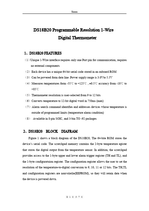
DS18B20Programmable Resolution1-WireDigital Thermometer1、DS18B20FEATURES(1)Unique1-Wire interface requires only one Port pin for communication,requires no external components(2)Each device has a unique64-bit serial code stored in an onboard ROM(3)Can be powered form data line.Power supply range is3.0Vto5.5V(4)Measures temperatures form-55℃to+125℃,±0.5℃accuracy from-10℃to +85℃(5)Thermometer resolution is user-selected from9to12bits(6)Converts temperature to12-bit digital word in750ms(max)(7)Alarm search command identifies and addresses devices whose temperature is outside of programmed limits(temperature alarm condition)(8)Available in8-pin SOIC,and3-bin TO-92packages2、DS18B20BLOCK DIAFRAMFigure1shows a block diagram of the DS18B20,The64-bite ROM stores the device’s serial code.The scratchpad memory contains the2-byte temperature egister that stores the digital output from the temperature sensor.In addition,the scratchpad provides access to the1-byte upper and lower alarm trigger register(TH and TL),and the1-byte configuratuion register.The configuration register allows the user to set the resolution of the temperature-to-digital conversion to9,10,11or12bits.The TH,TL and configuration registers are nonvolatile(EEPROM),so they will retain data when the device is powered down.Figure1block diagram of the DS18B203、DS18B20ROM COMMANDS(1)SEARCH ROM[0F0H]When a system is initially powered up,the master must identify the ROM codes of all slave devices on the bus,which allows the master to determine the number of slaves and their device types.The master learns the ROM codes through a process of elimination that requires the master to perform a Search ROM cycle as many times as necessary to identify all of the slave’s64-bit ROM devices.(2)READ ROM[55H]This command can only be used when there is one slave on the bus.It allows the bus master to read the slave`64-bit ROM code without using the Search ROM procedure.If this command is used when there is more than one slave present on the bus,a data collision will occur when all the slaves attempt to respond at the same time.(3)MATCH ROM[55H]The match ROM command followed by a64-bit ROM code sequence allows the bus master to address a specific DS18B20on a multidrop or single-drop bus.Only the DS18B20that exactly matches the64-bitROM code sequence will respond to thefunction command issued by the master;all other slaves on the bus will wait for a reset pulse.(4)SKIP ROM[0CCH]The master can use this command to address all devices on the bus simultaneously without sending out any ROM code information.Note that the Read Scratchpad command can follow the Skip ROM command only if there is a single slave device on the bus.In this case time is saved by allowing the master to read from the slave without sending the device’s64-bit ROM code.A Skip ROM command followed by a Read Scratchpad command will cause a data collision on the bus if there is more than one slave since multiple devices will attempt to transmit data simultaneously.(5)ALARM SEARCH[0ECH]The operation of this command is identical to the operation of the Search ROM command except that only slaves with a set alarm flag will respond.This command allows the master device to determine if any DS18B20s experienced an alarm condition during the most recent temperature conversion.Refer to the OPERATION-ALARM SIGNAING section for an explanation of alarm flag operation.(6)CONVERTT[44H]This command initiates a single temperature conversion.Following the conversion,the resulting thermal data is stored in the2-bute temperature register in the scratchpad memory and the DS18B20returns to its low-power idle state.If the device is being used in parasite power mode,within10us after this command is issued the master must enable a strong pullup on the1-Wire bus for the duration of the conversion as described in the POWERING THE DS18320section.If the DS18B20 is powered by an external supply,the master can issue read time slots after the Convert T command and the DS18B20will respond by transmitting a0while the temperature conversion is in Progress and a1when the conversion is done.In parasite power mode this notification technique cannot be used since the bus1is pulled high by the strong pullup during the conversion.(7)WRITE SCRACHPAD[4EH]This command allows the master to write3bytes of the data to the DS18B20’s scratchpad.The first data byte is writer into the TH register,the second byte is written into the TL register,and the third byte is written into the configuration register. Data must be transmitted least significant bit first.All three bytes must be written before the master issues a reset,or the data may be corrupted.(8)READ SCRACHPAD[0BEH]This command allows the master to read the contents of the scratchpad.The data transfer starts with the least significant bit of byte0and continues through the scratchpad until9byte(byte8-CRC)is read.The master may issue a reset to terminate reading at any time if only partof the scratchpad data is needed.(9)COPY SCRATCHPAD[48H]This command copies the contents of the scratchpad TH,TL and configuration registers to EEPROM.If the device is being used in parasite power mode,within 10us(max)after this command is issued the master must enable a strong pullup on the 1-Wire bus for at least10ms as described in the POWERING THE DS18B20section.(10)RECALL E2[B8H]This command recalls the alarm trigger values(TH and TL)and configuration data from EEPROM,respectively,in the scratchpad memory.The master device can issue read time slots following the Recall E2command and the DS18B20will indicate the status of the recall by transmitting0while the recall is in progress and1 when the recall is done.The recall operation happens automatically at power-up,so valid data is available in the scratchpad as soon as power is applied to the device.DS18B20单总线数字温度计1、DS18B20的特性(1)独特的单总线接口只占用一个I/O端口,而无需外围元件;(2)可以由总线提供电源,电压适用范围为3.0V~5.5V;(3)测量温度范围为-55℃~+125℃,在-10℃~+85℃范围内精度为±0.5℃;(4)每个DS18B20含有一个唯一的64位ROM编码;(5)用户可以通过编程实现9~12位的温度分辨率;(6)分辨率为12时最大转换时间为750ms;(7)报警搜索命令可识别哪片DS18B20温度超限;(8)采用3脚T0-92或8脚SOIC封装。
温湿度测量仪外文文献翻译、中英文翻译

外文翻译英文原文:Temperature and humidity measuring instrumentIntroductionTemperature and humidity measurement is a modern newly developed measurement field, especially the humidity measurement is to continue moving forward. Experienced a length method, dry and wet until today the course of the measurement, humidity measurement technology is maturing. Today, we are no longer satisfied with the measurement of the temperature and humidity, especially in some places to monitor directly the requirements of real-time measure and record the temperature and humidity changes in the whole process, and based on these changes identified during storage and transportation security, led to a new temperature and humidity measuring instrument was born. Temperature and humidity measuring instrument is the temperature and humidity parameters were measured according to a predetermined time interval stored in the internal memory, in the completion of the recording function will be coupled to a PC, use the adapter software data stored in accordance with values time analysis instrument. The instrument can determine the storage and transportation process, experiment process without any compromise product safety incident.MSP430F437 IntroducedThe MSP430 MCU main features are as follows:1)Ultra-low power consumption. MSP430 MCU supply voltage 1.8 to 3.6V low voltage RAM data retention mode power consumption of only 0.1uA active mode power 250uA/MIPS, IO input port leakage current of only 50nA.2)Powerful processing capability. The MSP430 MCU 16-bit microcontroller, reduced instruction set architecture with the most popular one clock cycle to execute an instruction, the MSP430 instruction speeds of up to 8MHz oscillator is 8MIPS.3)High-performance analog technology and a wealth of on-chip peripheral modules. The MSP430 monolithic organic combination of TI's high-performance analog technology, each member of the rich on-chip peripherals are integrated. Depending on the model of the different possible combinations of the following modules: watchdog,analog comparator A timer A, timer B, serial 0,1, hardware multiplier, LCD driver, 10/12/14-bit ADC, 12 DAC IIC bus, direct data access, port 1 to 6, the basic timer. 4)The system is stable. Power-on reset, first initiated by the DC0 CPU, to ensure that the program starts executing from the correct position to ensure crystal oscillator start-up and stabilization time. The software can then set the appropriate control bits of the register to determine the final system clock frequency. If the crystal oscillator is used as the CPU clock MCLK failure, the DCO will start automatically, in order to ensure the normal operation of the system. This structure and operational mechanism in the current series microcontroller is unique.5)Convenient and efficient development environment. MSP430 series OTP type, three types of FLASH-ROM, the domestic large-scale use FLASH. The development of these devices means, after the successful development of the OTP and ROM-type device using a dedicated emulator programmer or chip cover touch. FLASH type is very convenient development and debugging environment, because the device on-chip JTAG debug interface, as well as the electric flash FLASH memory using the first through the JTAG interface to download the program to the FLASH, run by the JTAG interface control program read the on-chip CPU status, and memory contents and other information for designers debug the entire development can be carried out in the same software integrated environment. Which only requires a PC and a JTAG debugger, without the need for a dedicated emulator and programmer. Temperature And Humidity SensorThe SHT7x temperature and humidity sensor characteristics are as follows:1)The temperature and humidity sensor signal is amplified conditioning, A / D converter, all integrated on one IIC bus interface;2)Given calibration relative humidity and temperature output;3)IIC bus with industry-standard digital output interface;4)With dewpoint calculation output function;5)With excellent long-term stability;6)Humidity value output resolution of 14 The temperature output resolution of 12 bits, and programmable;7)Small size (7.65 x 5.08 x 23.5mm) Surface Mount;8)Having reliable the CRC data transmission checking function;9)The chip load calibration coefficients can guarantee 100% interchangeability;AT25256 IntroductionTemperature and humidity data storage chip SPI interface uses ATMEL Corporation's low-voltage serial EEPROM AT25256. AT25256 is mainly applied to low-power occasion the internal accordance with 32K x 8-bit organization, can work at 3.3V, the maximum serial clock frequency as to 2.1MHz. Support for 64-byte page write mode and byte write mode. AT25256 by setting the write-protect pin / WP level to set the chip read-only or writable state. Serial Peripheral Interface (SPI) bus technology is a synchronous serial interface, the hardware features a strong, SPI software is quite simple, so that the CPU has more time to deal with other matters. SPI bus can be connected to multiple host MCU, equipped with SPI interface output devices, output devices, such as LCD drivers, A / D conversion and other peripherals can also be a simple connection to a single TTL shift register chip. The bus allows you to connect multiple devices, but only one device at any moment as the host.SPI bus clock line is controlled by the host, in addition to data lines: host input / output line from the machine and the host output / slave input line. Host and which slave communication through the slave strobe line selection.Application SPI system can be simple, complex and can take many forms: (1) a host MCU and the slave MCU; (2) multiple MCU are connected to each other into a multi-host system; (3) a host MCU and slave peripherals.Segment LCD Display PrincipleLCD display principle is to use the physical characteristics of the liquid crystal born, when power is turned on, arranged order so light by; arranged confusion is not energized, to prevent the light to pass through. Light to pass through and not through a combination of an image is displayed on the screen. In layman's terms, the liquid crystal display is the middle of the two glass clip a layer of liquid crystal material, the liquid crystal material to change their light transmission in the signal under the control of the state, so you can see the image in front of the glass panel. LCD ambient light to display information, the LCD itself is not self-luminous, LCD power consumption is very low, more suitable for single-chip low-power applications. In addition, the LCD can only use low-frequency AC voltage drive, the DC voltage will damage the LCD. There are many types of LCD segment liquid crystal character LCD, graphical LCD. Segment LCD inexpensive, simple to use, is widely used in a variety of microcomputer application system.MSP430 LCD driver module has four driving method, respectively, for static drive, 2MUX drive, 3MUX, Drivers, 4MUX drive. Static driving method, in additionto the public badly in need of a pin, each section of the drive each one pin. If the design involves a lot of number of segments, you need to take up the many pin. In order to reduce the pin number, you can select multiple drive needed: 2MUX drive, drive, 3MUX 4MUX driving method. Increase the number of public-pole, can greatly reduce the number of pins. Need to drive more segments, the more obvious effects. ConclusionThe design requirements to simultaneously detect the temperature and humidity. From the temperature and humidity sensor signal IIC bus to enter MSP430F437 MSP430F437, temperature and humidity data on the one hand to send the LCD display; the other hand, the temperature and humidity data is stored in AT25256 stored temperature and humidity data can be transmitted via RS232 bus to the PC, In the PC application, you can curve shows the temperature and humidity data, and can print the report.This design uses the MSP430 MCU measurement of temperature and humidity, display, storage, transmission, printing and other functions. But also through the button on the temperature and humidity measurement time interval, whether storage, starting time and other parameters set. In addition, the entire system can be connected to external 9V DC power supply, you can use a 9V lithium battery-powered, low-power design ultra-low power MSP430 MCU, and program design, making the whole system very power, particularly suitable for hand-held meter.中文翻译:温湿度测量仪1 引言温湿度测量是现代测量新发展出来的一个领域,尤其湿度的测量更是不断前进。
数字温度计外文翻译

附录二外文资料翻译资料原文DS18B20Programmable Resolution1-Wire Digital ThermometerDESCRIPTIONThe DS18B20 Digital Thermometer provides 9 to 12–bit centigrade temperature measurements and has an alarm function with nonvolatile user-programmable upper and lower trigger points. The DS18B20 communicates over a 1-Wire bus that by definition requires only one data line (and ground) for communication with a central microprocessor. It has an operating temperature range of –55℃ to +125°C and is accurate to ±0.5℃ over the range of –10℃ to +85℃. In addition, the DS18B20 can derive power directly from the data line (“parasite power”), eliminating the need for an external power supply.Each DS18B20 has a unique 64-bit serial code, which allows multiple DS18B20s to function on the same 1–wire bus; thus, it is simple to use one microprocessor to control many DS18B20s distributed over a large area. Applications that can benefit from this feature include HVAC environmental controls,temperature monitoring systems inside buildings, equipment ormachinery, and process monitoring and control systems.OVERVIEWFigure 1 shows a block diagram of the DS18B20, and pin descriptions are given in Table 1. The 64-bit ROM stores the device’s unique serial code. The scratchpad memory contains the 2-byte temperature register that stores the digital output from the temperature sensor. In addition, the scratchpad provides access to the 1-byte upper and lower alarm trigger registers (TH and TL), and the 1-byte configuration register. The configuration register allows the user to set the resolution of the temperature-to-digital conversion to 9, 10, 11, or 12 bits. The TH, TL and configuration registers are nonvolatile (EEPROM), so they will retain data when the device is powered down.The DS18B20 uses Dallas’exclusive 1-Wire bus protocol that implements bus communication using one control signal. The control line requires a weak pullup resistor since all devices are linked to the bus via a 3-state or open-drain port (the DQ pin in the case of the DS18B20). In this bus system, the microprocessor (the master device) identifies and addresses devices on the bus using each device’s unique 64-bit code. Because each device has a unique code, the number of devices that can be addressed on one bus is virtually unlimited. The 1-Wire bus protocol, including detailed explanations of the commands and“time slots,” is covered in the 1-WIRE BUS SYSTEM section of this datasheet.Another feature of the DS18B20 is the ability to operate without an external power supply. Power is instead supplied through the 1-Wire pullup resistor via the DQ pin when the bus is high. The high bus signal also charges an internal capacitor (Cpp), which then supplies power to the device when the bus is low. This method of deriving power from the 1-Wire bus is referred to as “parasite power.” As an alternative, the DS18B20 may also be powered by an external supply on VDD.OPERATION — MEASURING TEMPERATUREThe core functionality of the DS18B20 is its direct-to-digital temperature sensor. The resolution of the temperature sensor is user-configurable to 9, 10, 11, or 12 bits, corresponding to increments of 0.5℃, 0.25℃, 0.125℃, and 0.0625℃, respectively. The default resolution at power-up is 12-bit. The DS18B20 powers-up in a low-power idle state; to initiate a temperature measurement and A-to-D conversion, the master must issue a Convert T [44h] command. Following the conversion, the resulting thermal data is stored in the 2-byte temperature register in the scratchpad memory and the DS18B20 returns to its idle state. If the DS18B20 is powered by an external supply, the master can issue “read time slots” (see the 1- WIRE BUS SYSTEM section) after the Convert T command and the DS18B20 will respond by transmitting 0 while the temperature conversion is in progress and 1 when the conversion is done. If the DS18B20 is powered with parasite power, this notification technique cannot be used since the bus must be pulled high by a strong pullup during the entire temperature conversion. The bus requirements for parasite power are explained in detail in the POWERING THE DS18B20 section of this datasheet.POWERING THE DS18B20The DS18B20 can be powered by an external supply on the VDD pin, or it can operate in “parasite power”mode, which allows the DS18B20 to function without a local external supply. Parasite power is very useful for applications that require remote temperature sensing or that are very space constrained. Figure 1 shows the DS18B20’s parasite-power control circuitry, which “steals” power from the 1-Wire bus via the DQ pin when the bus is high. The stolen charge powers the DS18B20 while the bus is high, and some of the charge is stored on the parasite power capacitor (CPP) to provide power when the bus is low. When the DS18B20 is used in parasite power mode, the VDD pin must be connected to ground. In parasite power mode, the 1-Wire bus and CPP can provide sufficient current to the DS18B20 for most operations as long as the specified timing and voltage requirements are met (refer to the DC ELECTRICAL CHARACTERISTICS and the AC ELECTRICAL CHARACTERISTICS sections of this data sheet). However, when the DS18B20 is performing temperature conversions or copying data from the scratchpad memory to EEPROM, the operating current can be as high as 1.5mA. This current can cause an unacceptable voltage drop across the weak 1-Wire pullup resistor and is more current than can be supplied by CPP. To assure that the DS18B20 has sufficient supply current, it is necessary to provide a strong pullup on the 1-Wire bus whenever temperature conversions are taking place or data is being copied from the scratchpad to EEPROM. This can be accomplished by using a MOSFET to pull thebus directly to the rail as shown in Figure 4. The 1-Wire bus must be switched to the strong pullup within 10μs(max) after a Convert T [44h] or Copy Scratchpad [48h] command is issued, and the bus must be held high by the pullup for the duration of the conversion (tconv) or data transfer (twr = 10ms). No other activity can take place on the 1-Wire bus while the pullup is enabled.The DS18B20 can also be powered by the conventional method of connecting an external power supply to the VDD pin, as shown in Figure 5. The advantage of this method is that the MOSFET pullup is not required, and the 1-Wire bus is free to carry other traffic during the temperature conversion time.The use of parasite power is not recommended for temperatures above +100℃ since the DS18B20 may not be able to sustain communications due to the higher leakage currents that can exist at these temperatures. For applications in which such temperatures are likely, it is strongly recommended that the DS18B20 be powered by an external power supply.In some situations the bus master may not know whether the DS18B20s on the bus are parasite powered or powered by external supplies. The master needs this information to determine if the strong bus pullup should be used during temperature conversions. To get this information, the master can issue a Skip ROM [CCh] command followed by a Read Power Supply [B4h] command followed by a “read time slot”. During the read time slot, parasite powered DS18B20s will pull the bus low, and externally powered DS18B20s will let the bus remain high. If the bus is pulled low, the master knows that it must supply the strong pullup on the 1-Wire bus during temperature conversions.MEMORYThe DS18B20’s memory is organized as shown in Figure 7. The memory consists of an SRAM scratchpad with nonvolatile EEPROM storage for the high and low alarm trigger registers (TH and TL) and configuration register. Note that if the DS18B20 alarm function is not used, the TH and TL registers can serve as general-purpose memory. All memory commands are described in detail in the DS18B20 FUNCTION COMMANDS section. Byte 0 and byte 1 of the scratchpad contain the LSB and the MSB of the temperature register, respectively. These bytes are read-only. Bytes 2 and 3 provide access to TH and TL registers. Byte 4 contains the configuration register data, which is explained in detail in the CONFIGURATION REGISTER section of this datasheet. Bytes 5, 6, and 7 are reserved for internal use by the device and cannot be overwritten; these bytes will return all 1s when read.Byte 8 of the scratchpad is read-only and contains the cyclic redundancy check (CRC) code for bytes 0 through 7 of the scratchpad. The DS18B20 generates this CRC using the method described in the CRC GENERATION section.Data is written to bytes 2, 3, and 4 of the scratchpad using the Write Scratchpad [4Eh] command; the data must be transmitted to the DS18B20 starting with the least significant bit of byte 2. To verify data integrity, the scratchpad can be read (using the Read Scratchpad [BEh] command) after the data is written. When reading the scratchpad, data is transferred over the 1-Wire bus starting with the leastsignificant bit of byte 0. To transfer the TH, TL and configuration data from the scratchpad to EEPROM, the master must issue the Copy Scratchpad [48h] command. Data in the EEPROM registers is retained when the device is powered down; at power-up the EEPROM data is reloaded into the corresponding scratchpad locations. Data can also be reloaded from EEPROM to the scratchpad at any time using the Recall E2 [B8h] command. The master can issue read time slotsfollowing the Recall E2 command and the DS18B20 will indicate the status of the recall by transmitting 0 while the recall is in progress and 1 when the recall is done.CRC GENERATIONCRC bytes are provided as part of the DS18B20’s 64-bit ROM code and in the 9th byte of the scratchpad memory. The ROM code CRC is calculated from the first 56 bits of the ROM code and is contained in the most significant byte of the ROM. The scratchpad CRC is calculated from the data stored in the scratchpad, and therefore it changes when the data in the scratchpad changes. The CRCs provide the bus master with a method of data validation when data is read from the DS18B20. To verify that data has been read correctly, the bus master must re-calculate the CRC from the received data and then compare this value to either the ROM code CRC (for ROM reads) or to the scratchpad CRC (for scratchpad reads). If the calculated CRC matches the read CRC, the data has been received error free. The comparison of CRC values and the decision to continue with an operation are determined entirely by the bus master. There is no circuitry inside the DS18B20 that prevents a command sequence from proceeding if the DS18B20 CRC (ROM or scratchpad) does not match the value generated by the bus master.The equivalent polynomial function of the CRC (ROM or scratchpad) is:CRC = X8 + X5 + X4 + 1The bus master can re-calculate the CRC and compare it to the CRC values from the DS18B20 using the polynomial generator shown in Figure 9. This circuit consists of a shift register and XOR gates, and the shift register bits are initialized to 0. Starting with the least significant bit of the ROM code or the least significant bit of byte 0 in the scratchpad, one bit at a time should shifted into the shift register. After shifting in the 56th bit from the ROM or the most significant bit of byte 7 from the scratchpad, the polynomial generator will contain the re-calculated CRC. Next, the 8-bit ROM code or scratchpad CRC from the DS18B20 must be shifted into the circuit. At this point, if the re-calculated CRC was correct, the shift register will contain all 0s.HARDWARE CONFIGURATIONThe 1-Wire bus has by definition only a single data line. Each device (master or slave) interfaces to the data line via an open-drain or 3-state port. This allows each device to “release” the data line when the device is not transmitting data so the bus is available for use by another device. The 1-Wire port of the DS18B20 (the DQ pin) is open drain with an internal circuit equivalent to that shown in Figure 10.The 1-Wire bus requires an external pullup resistor of approximately 5kΏ; thus, the idle state for the 1-Wire bus is high. If for any reason a transaction needs to be suspended, the bus MUST be left in the idle state if the transaction is to resume. Infinite recovery time can occur between bits so long as the 1-Wire bus is in the inactive (high) state during the recovery period. If the bus is held low for more than 480μs, all components on the bus will be reset.资料翻译DS18B20可编程分辨率的单总线®数字温度计说明DS18B20 数字温度计提供9-12 位摄氏温度测量而且有一个由高低电平触发的可编程的不因电源消失而改变的报警功能。
温湿度测量仪外文文献翻译、中英文翻译
外文翻译英文原文:Temperature and humidity measuring instrumentIntroductionTemperature and humidity measurement is a modern newly developed measurement field, especially the humidity measurement is to continue moving forward. Experienced a length method, dry and wet until today the course of the measurement, humidity measurement technology is maturing. Today, we are no longer satisfied with the measurement of the temperature and humidity, especially in some places to monitor directly the requirements of real-time measure and record the temperature and humidity changes in the whole process, and based on these changes identified during storage and transportation security, led to a new temperature and humidity measuring instrument was born. Temperature and humidity measuring instrument is the temperature and humidity parameters were measured according to a predetermined time interval stored in the internal memory, in the completion of the recording function will be coupled to a PC, use the adapter software data stored in accordance with values time analysis instrument. The instrument can determine the storage and transportation process, experiment process without any compromise product safety incident.MSP430F437 IntroducedThe MSP430 MCU main features are as follows:1)Ultra-low power consumption. MSP430 MCU supply voltage 1.8 to 3.6V low voltage RAM data retention mode power consumption of only 0.1uA active mode power 250uA/MIPS, IO input port leakage current of only 50nA.2)Powerful processing capability. The MSP430 MCU 16-bit microcontroller, reduced instruction set architecture with the most popular one clock cycle to execute an instruction, the MSP430 instruction speeds of up to 8MHz oscillator is 8MIPS.3)High-performance analog technology and a wealth of on-chip peripheral modules. The MSP430 monolithic organic combination of TI's high-performance analog technology, each member of the rich on-chip peripherals are integrated. Depending on the model of the different possible combinations of the following modules: watchdog,analog comparator A timer A, timer B, serial 0,1, hardware multiplier, LCD driver, 10/12/14-bit ADC, 12 DAC IIC bus, direct data access, port 1 to 6, the basic timer. 4)The system is stable. Power-on reset, first initiated by the DC0 CPU, to ensure that the program starts executing from the correct position to ensure crystal oscillator start-up and stabilization time. The software can then set the appropriate control bits of the register to determine the final system clock frequency. If the crystal oscillator is used as the CPU clock MCLK failure, the DCO will start automatically, in order to ensure the normal operation of the system. This structure and operational mechanism in the current series microcontroller is unique.5)Convenient and efficient development environment. MSP430 series OTP type, three types of FLASH-ROM, the domestic large-scale use FLASH. The development of these devices means, after the successful development of the OTP and ROM-type device using a dedicated emulator programmer or chip cover touch. FLASH type is very convenient development and debugging environment, because the device on-chip JTAG debug interface, as well as the electric flash FLASH memory using the first through the JTAG interface to download the program to the FLASH, run by the JTAG interface control program read the on-chip CPU status, and memory contents and other information for designers debug the entire development can be carried out in the same software integrated environment. Which only requires a PC and a JTAG debugger, without the need for a dedicated emulator and programmer. Temperature And Humidity SensorThe SHT7x temperature and humidity sensor characteristics are as follows:1)The temperature and humidity sensor signal is amplified conditioning, A / D converter, all integrated on one IIC bus interface;2)Given calibration relative humidity and temperature output;3)IIC bus with industry-standard digital output interface;4)With dewpoint calculation output function;5)With excellent long-term stability;6)Humidity value output resolution of 14 The temperature output resolution of 12 bits, and programmable;7)Small size (7.65 x 5.08 x 23.5mm) Surface Mount;8)Having reliable the CRC data transmission checking function;9)The chip load calibration coefficients can guarantee 100% interchangeability;AT25256 IntroductionTemperature and humidity data storage chip SPI interface uses ATMEL Corporation's low-voltage serial EEPROM AT25256. AT25256 is mainly applied to low-power occasion the internal accordance with 32K x 8-bit organization, can work at 3.3V, the maximum serial clock frequency as to 2.1MHz. Support for 64-byte page write mode and byte write mode. AT25256 by setting the write-protect pin / WP level to set the chip read-only or writable state. Serial Peripheral Interface (SPI) bus technology is a synchronous serial interface, the hardware features a strong, SPI software is quite simple, so that the CPU has more time to deal with other matters. SPI bus can be connected to multiple host MCU, equipped with SPI interface output devices, output devices, such as LCD drivers, A / D conversion and other peripherals can also be a simple connection to a single TTL shift register chip. The bus allows you to connect multiple devices, but only one device at any moment as the host.SPI bus clock line is controlled by the host, in addition to data lines: host input / output line from the machine and the host output / slave input line. Host and which slave communication through the slave strobe line selection.Application SPI system can be simple, complex and can take many forms: (1) a host MCU and the slave MCU; (2) multiple MCU are connected to each other into a multi-host system; (3) a host MCU and slave peripherals.Segment LCD Display PrincipleLCD display principle is to use the physical characteristics of the liquid crystal born, when power is turned on, arranged order so light by; arranged confusion is not energized, to prevent the light to pass through. Light to pass through and not through a combination of an image is displayed on the screen. In layman's terms, the liquid crystal display is the middle of the two glass clip a layer of liquid crystal material, the liquid crystal material to change their light transmission in the signal under the control of the state, so you can see the image in front of the glass panel. LCD ambient light to display information, the LCD itself is not self-luminous, LCD power consumption is very low, more suitable for single-chip low-power applications. In addition, the LCD can only use low-frequency AC voltage drive, the DC voltage will damage the LCD. There are many types of LCD segment liquid crystal character LCD, graphical LCD. Segment LCD inexpensive, simple to use, is widely used in a variety of microcomputer application system.MSP430 LCD driver module has four driving method, respectively, for static drive, 2MUX drive, 3MUX, Drivers, 4MUX drive. Static driving method, in additionto the public badly in need of a pin, each section of the drive each one pin. If the design involves a lot of number of segments, you need to take up the many pin. In order to reduce the pin number, you can select multiple drive needed: 2MUX drive, drive, 3MUX 4MUX driving method. Increase the number of public-pole, can greatly reduce the number of pins. Need to drive more segments, the more obvious effects. ConclusionThe design requirements to simultaneously detect the temperature and humidity. From the temperature and humidity sensor signal IIC bus to enter MSP430F437 MSP430F437, temperature and humidity data on the one hand to send the LCD display; the other hand, the temperature and humidity data is stored in AT25256 stored temperature and humidity data can be transmitted via RS232 bus to the PC, In the PC application, you can curve shows the temperature and humidity data, and can print the report.This design uses the MSP430 MCU measurement of temperature and humidity, display, storage, transmission, printing and other functions. But also through the button on the temperature and humidity measurement time interval, whether storage, starting time and other parameters set. In addition, the entire system can be connected to external 9V DC power supply, you can use a 9V lithium battery-powered, low-power design ultra-low power MSP430 MCU, and program design, making the whole system very power, particularly suitable for hand-held meter.中文翻译:温湿度测量仪1 引言温湿度测量是现代测量新发展出来的一个领域,尤其湿度的测量更是不断前进。
基于单片机的温度控制外文文献及中文翻译
Temperature Control Using a Microcontroller:An Interdisciplinary Undergraduate Engineering Design ProjectJames S. McDonaldDepartment of Engineering ScienceTrinity UniversitySan Antonio, TX 78212Abstract:This paper describes an interdisciplinary design project which was done under the author' s supervision by a group of four senior students in the Department of Engineering Science at Trinity University. The objective of the project was to develop a temperature control system for an air-filled chamber. The system was to allow entry of a desired chamber temperature in a prescribed range and to exhibit overshoot and steady-state temperature error of less than 1 degree Kelvin in the actual chamber temperature step response. The details of the design developed by this group of students, based on a Motorola MC68HC05 family microcontroller, are described. The pedagogical value of the problem is also discussed through a description of some of the key steps in the design process .It is shown that the solution requires broad knowledge drawn from several engineering disciplines including electrical, mechanical, and control systems engineering.1 IntroductionThe design project which is the subject of this paper originated from a real-world application.A prototype of a microscope slide dryer had been developed around an OmegaTM model -390 temperature controller, and the objective was to develop a custom temperature control system to replace the Omega system. The motivation was that a custom controller targeted specifically for the application should be able to achieve the same functionality at a much lower cost, as theOmega system is unnecessarily versatile and equipped to handle a wide variety of applications.The mechanical layout of the slide dryer prototype is shown in Figure 1. The main element of the dryer is a large, insulated, air-filled chamber in which microscope slides, each with a tissue sample encased in paraffin, can be set on caddies. In order that the paraffin maintain the proper consistency, the temperature in the slide chamber must be maintained at a desired (constant) temperature. A second chamber (the electronics enclosure) houses a resistive heater and the temperature controller, and a fan mounted on the end of the dryer blows air across the heater, carrying heat into the slide chamber. This design project was carried out during academic year 1996 一97 by four students under the author5 s supervision as a Senior Design project in the Department of Engineering Science at Trinity University. The purpose of this paper is to describe the problem and the students5 solution in some detail, and to discuss some of the pedagogical opportunities offered by an interdisciplinary design project of this type. The students' own report was presented at the 1997 National Conference on Undergraduate Research [1]. Section 2 gives a more detailed statement of the problem, including performance specifications, and Section 3 describes the students, design. Section 4 makes up the bulk of the paper, and discusses in some detail several aspects of the design process which offer unique pedagogical opportunities. Finally, Section 5 offers some conclusions.2 Problem StatementThe basic idea of the project is to replace the relevant parts of the functionality of an Omega -390 temperature controller using a custom-designed system. The application dictates that temperature settings are usually kept constant for long periods of time, but if s nonetheless important that step changes be tracked in a “reasonable” manner. Thus the main requirements boil down to• allowing a chamber temperature set-point to be entered,• displaying both set-point and actual temperatures, and• tracking step changes in set-point temperature with acceptable rise time, steady-state error, and overshoot.Top ViewFront View10.25” 6.25” Figure 1. Slide diyer ineclicmical layouiAlthough not explicitly a part of the specifications in Table 1, it was clear that the customer desired digital displays of set-point and actual temperatures, and that set-point temperature entry should be digital as well (as opposed to, say, through a potentiometer setting).3 System DesignThe requirements for digital temperature displays and setpoint entry alone are enough to dictate that a microcontrollerbased design is likely the most appropriate・ Figure 2 shows a block diagram of the students5 design.Figure 2. Temperature controller hardwcuv block diagramThe microcontroller, a MotorolaMC68HC705B16 (6805 for short), is the heart of the system. It accepts inputs from a simple four-key keypad which allow specification of the set-point temperature, and it displays both set-point and measured chamber temperatures using two-digit seven-segment LED displays controlled by a display driver. All these inputs and outputs are acmodated by parallel ports on the 6805. Chamber temperature is sensed using a pre-calibrated thermistor and input via one of the 6805' s analog-to-digital inputs. Finally, a pulse-width modulation (PWM) output on the 6805 is used to drive a relay which switches line power to the resistive heater off and on.Figure 3 shows a more detailed schematic of the electronics and their interfacing to the 6805. The keypad, a Storm 3K041103, has four keys which are interfaced to pins PA0{ PA3 of Port A, configured as inputs. One key functions as a mode switch. Two modes are sup ported: set mode and run mode. In set mode two of the other keys are used to specify the set-point temperature: one increments it and one decrements. The fourth key is unused at present. The LED displays aredriven by a Harris Semiconductor ICM7212 display driver interfaced to pins PB0IPB6 of Port B, configured as outputs. The temperature-sensing thermistor drives, through a voltage divider, pin ANO (one of eight analog inputs). Finally, pin PLMA (one of two PWM outputs) drives the heater relay.Figure 3. Schematic ofinicrocontroUer boardSoftware on the 6805 implements the temperature control algorithm, maintains the temperature displays, and alters the set-point in response to keypad inputs. Because it is not plete at this writing, software will not be discussed in detail in this paper. The control algorithm in particular has not been determined, but it is likely to be a simple proportional controller and certainly not more plex than a PID. Some control design issues will be discussed in Section 4,however.4 The Design ProcessAlthough essentially the project is just to build a thermostat, it presents many nice pedagogical opportunities. The knowledge and experience base of a senior engineering undergraduate are just enough to bring him or her to the brink of a solution to various aspects of the problem. Yet, in each case, realworld considerations plicate the situation significantly.Fortunately these plications are not insurmountable, and the result is a very beneficial design experience. The remainder of this section looks at a few aspects of the problem which present the type of learning opportunity just described. Section 4.1 discusses some of the features of a simplified mathematical model of the thermal properties of the system and how it can be easily validated experimentally. Section 4.2 describes how realistic control algorithm designs can be arrived at using introductory concepts in control design. Section 4.3 points out some important deficiencies of such a simplified modeling/control design process and how they can be overe through simulation. Finally, Section 4.4 gives an overview of some of the microcontroller-related design issues which arise and learning opportunities offered.4.1 MathematicalModelLumped-element thermal systems are described in almost any introductory linear control systems text, and just this sort of model is applicable to the slide dryer problem. Figure 4 shows a second-order lumped-element thermal model of the slide dryer. The state variables are the temperatures Ta of the air in the box and Tb of the box itself. The inputs to the system are the power output q(t) of the heater and the ambient temperature T¥. ma and mb are the masses of the air and the box, respectively, and Ca and Cb their specific heats. p1 and JJ2 are heat transfercoefficients from the air to the box and from the box to the external world, respectively.If s not hard to show that the (linearized) state equationscorresponding to Figure 4 are 〃皿方 - 〃坊-“1(爲r — Tb) (1) “1(爲一 Tb) _ 'Tb — TJ (2) Taking Laplace transforms of (1) and (2) and solving for Ta(s), which is the output of interest, gives the following open-loop model of the thermal system:加)•K(x z s + 1) 1 Twhere K is a constant and D(s) is a second-order polynomial.K, tz, and the coefficients of D(s) are functions of the variousparameters appearing in (1) and (2).Of course the various parameters in (1) and(2) are pletely unknown, but if s not hard to show that, regardless of their values, D(s) has two real zeros. Therefore the main transfer function of interest (which is the one from Q(s), since we J II assume constant ambient temperature) can be written_ 爲⑸ _ Kg+ 1)力 W (^15+1)(^25 4- 1)Moreover, it' s not too hard to show that 1 =tp1 <1=tz <1 =tp2, i.e., that the zero lies between the two poles. Both of these are excellent exercises for the student, and the result is the openloop pole-zero diagram of Figure 5.q ⑴Figure 4. Luinped-elemeiu the/刀modelaqObtaining a plete thermal model, then, is reduced to identifying the constant K and the three unknown time constants in (3). Four unknown parameters is quite a few, but simple experiments show that 1=tp1 _ Utz; 1=tp2 so that tz;tp2 _ 0 are good approximations. Thus the open-loop system is essentially first-order and can therefore be writtenK%($)- ⑷(where the subscript p1 has been dropped).Simple open-loop step response experiments show that,for a wide range of initial temperatures and heat inputs, K _0:14 _=W and t _ 295 s.14.2 Control System DesignUsing the first-order model of (4) for the open-loop transfer function Gaq(s) and assuming for the moment that linear control of the heater power output q(t) is possible, the block diagram of Figure 6 represents the closed-loop system. Td(s) is the desired, or set-point, temperature,C(s) is the pensator transfer function, and Q(s) is the heater output in watts.Given this simple situation, introductory linear control design tools such as the root locus method can be used to arrive at a C(s) which meets the step response requirements on rise time, steady-state error, and overshoot specified in Table 1 .The upshot, of course, is that a proportional controller with sufficient gain can meet all specifications. Overshoot is impossible, and increasing gains decreases both steady-state error and rise time.Unfortunately, sufficient gain to meet the specifications may require larger heat outputs than the heater is capable of producing. This was indeed the case for this system, and the result is that the rise time specification cannot be met. It is quite revealing to the student how useful such an oversimplified model, carefully arrived at, can be in determining overall performance limitations.4.3 Simulation ModelGross performance and its limitations can be determined using the simplified model of Figure 6, but there are a number of other aspects of the closed-loop system whose effects on performance are not so simply modeled. Chief among these are• quantization error in analog -to-digital conversion of the measured temperature and-the use of PWM to control the heater.Both of these are nonlinear and time-varying effects, and the only practical way to study them is through simulation (or experiment, of course).Figure 7 shows a SimulinkTM block diagram of the closed-loop system which incorporates these effects. A/D converter quantization and saturation are modeled using standard Simulink quantizer乙(s)Figure 6. Simplified block diagram of the closed-loop systemand saturation blocks. Modeling PWM is more plicated and requires a custom S-function to represent it.Figure 7. Siimilink block diagram of closed-loop systemThis simulation model has proven particularly useful in gauging the effects of varying the basic PWM parameters and hence selecting them appropriately. (I.e., the longer the period, the larger the temperature error PWM introduces. On the other hand, a long period is desirable to avoid excessive relay “chatter,” among other things.) PWM is often difficult for students to grasp, and the simulation model allows an exploration of its operation and effects which is quite revealing.4.4 The MicrocontrollerSimple closed-loop control, keypad reading, and display control are some of the classic applications of microcontrollers, and this project incorporates all three. It is therefore an excellent all-around exercise in microcontroller applications. In addition, because the project is to produce an actual packaged prototype, it won, t doto use a simple evaluation board with the I/O pins jumpered to the target system. Instead, if s necessary to develop a plete embedded application. This entails the choice of an appropriate part from the broad range offered in a typical microcontroller family and learning to use a fairly sophisticated development environment. Finally, a custom printed-circuit board for the microcontroller and peripherals must be designed and fabricated.Microcontroller Selection. In view of existing local expertise, the Motorola line of microcontrollers was chosen for this project. Still, this does not narrow the choice down much. A fairly disciplined study of system requirements is necessary to specify which microcontroller, out of scores of variants, is required for the job. This is difficult for students, as they generally lack the experience and intuition needed as wellas the perseverance to wade through manufacturers J selection guides.Part of the problem is in choosing methods for interfacing the various peripherals (e.g., what kind of display driver should be used?). A study of relevant Motorola application notes [2, 3, 4] proved very helpful in understandingwhat basic approaches are available, and what microcontroller/peripheral binations should be considered.The MC68HC705B16 was finally chosen on the basis of its availableA/D inputs and PWMoutputs as well as 24 digital I/O lines. In retrospect this is probably overkill, as only one A/D channel, one PWM channel, and 11 I/O pins are actually required (see Figure 3). The decision was made to err on the safe side because a plete development system specific to the chosen part was necessary, and the project budget did not permit a second such system to be purchased should the first prove inadequate.Microcontroller Application Development. Breadboarding of the peripheral hardware, development of microcontroller software, and final debugging and testing of a custom printed-circuit board for the microcontroller and peripherals all require a development environment of some kind. The choice of a development environment, like that of the microcontroller itself, can be bewildering and requires some faculty expertise. Motorola makes three grades of development environment ranging from simple evaluation boards (at around $100) to full-blown real-time in-circuit emulators (at more like $7500). The middle option was chosen for this project: the MMEVS, which consists of _ a platform board (which supports all 6805-family parts), _ an emulator module (specific to B-series parts), and _ a cable and target head adapter (package-specific). Overall, the system costs about $900 and provides, with some limitations, in-circuit emulation capability. It also es with the simple but sufficient software development environment RAPID [5].Students find learning to use this type of system challenging, but the experience they gain in real-world microcontroller application development greatly exceeds the typical first-course experience usingsimple evaluation boards.Printed-Circuit Board. The layout of a simple (though definitely not trivial) printed-circuit board is another practical learning opportunity presented by this project. The final board layout, with package outlines, is shown (at 50% of actual size) in Figure & The relative simplicity of the circuit makes manual placement and routing practical—in fact, it likely gives better results than automatic in an application like this—and the student is therefore exposed to fundamental issues of printed-circuit layout and basic design rules. The layout software used was the very nice package pcb,2 and the board was fabricated in-house with the aid of our staff electronics technician.Figure 8. Printed-circuit layout for imcrocoutroUer board中文时:单片机温度控制:一个跨学科的本科生工程设廿顶目JamesS.McDonald工程科学系三一大学德克萨斯州圣安东尼奥市78212摘嬰:本文所描述的是作者领导由皿个三一大学高年级学生组成的01臥进行的一个跨学科工程项目的设廿。
外文翻译----数字温湿度传感器(SHT 1x SHT 7x)
- Ultra low power consumption
- Surface mountable or 4-pin fully interchangeable
- Small size
- Automatic power down
SHT1x / SHT7x Product Summary
The SHTxx is a single chip relative humidity and temperature multi sensor module comprising a calibrated digital output. Application of industrial CMOS processes with
patented micro-machining (CMOSens® technology) ensures highest reliability and excellent long term stability. The device includes a capacitive polymer sensing element for relative humidity and a bandgap temperature sensor. Both are seamlessly coupled to a 14bit analog to digital converter and a serial interface circuit on the same chip. This results in superior signal quality, a fast response time and insensitivity to external disturbances (EMC) at a very competitive price.Each SHTxx is individually calibrated in a precision humidity chamber with a chilled mirror hygrometer as reference. The calibration coefficients are programmed into the OTP memory. These coefficients are used internally during measurements to calibrate the signals from the sensors. The 2-wire serial interface and internal voltage regulation allows easy and fast system integration. Its tiny size and low power consumption makes it the ultimate choice for even the most demanding applications.The device is supplied in eith surface-mountable LCC (Leadless Chip Carrier) or as a pluggable 4-pin single-in-line type package. Customer specific packaging options may beavailable on request.
数字温度传感器毕业论文中英文资料外文翻译文献[管理资料]
毕业论文中英文资料外文翻译文献外文资料DS1722 Digital ThermometerWith scientific and technological progress and development of the types of temperature sensors increasingly wide range of application of the increasingly widespread, and the beginning analog toward digital, single-bus, dual-bus and bus-3 direction. And the number of temperature sensors because they apply to all microprocessor interface consisting of automatic temperature control system simulation can be overcome sensor and microprocessor interface need signal conditioning circuit and A / D converters advant ages of the drawbacks, has been widely used in industrial control, electronic transducers, medical equipment and other temperature control system. Among them, which are more representative of a digital temperature sensor DS18B20, MAX6575, the DS1722, MAX6636 other. This paper introduces the DS1722 digital temperature sensor characteristics, the use of the method and its timing. Internal structure and other relevant content.FEATURES:Temperature measurements require no external components;Measures temperatures from -55°C to +120°C. Fahrenheit equivalent is -67°F to +248°F;Thermometer accuracy is ±°C;Thermometer resolution is configurable from 8 to 12 bits (°C to °C resolution);Data is read from/written to via a Motorola Serial Peripheral Interface (SPI) or standard 3-wire serial interface;Wide analog power supply range ( - );Separate digital supply allows for logic;Available in an 8-pin SOIC (150 mil), 8-pin USOP, and flip chip package;PIN ASSIGNMENTFIGURE 1 PIN ASSIGNMENTPIN DESCRIPTION:SERMODE - Serial Interface Mode.CE - Chip Enable.SCLK - Serial Clock.GND – Ground.VDDA - Analog Supply Voltage.SDO - Serial Data Out.SDI - Serial Data In.VDDD - Digital Supply Voltage.DESCRIPTION:The DS1722 Digital Thermometer and Thermostat with SPI/3-Wire Interface provides temperature readings which indicate the temperature of the device. No additional components are required; the device is truly a temperature-to-digital converter. Temperature readings are communicated from the DS1722 over a Motorola SPI interface or a standard 3-wire serial interface. The choice of interface standard is selectable by the user. For applications that require greater temperature resolution, the user can adjust the readout resolution from 8 to 12 bits. This is particularly useful in applications where thermal runaway conditions must be detected quickly.For application flexibility, the DS1722 features a wide analog supply rail of - . A separate digital supply allows a range of to . The DS1722 is available in an 8-pin SOIC (150-mil), 8-pin USOP, and flip chip package.Applications for the DS1722 include personal computers/servers/workstations, cellular telephones, office equipment, or any thermally-sensitive system.OVERVIEW:A block diagram of the DS1722 is shown in Figure 2. The DS1722 consists offour major components:1. Precision temperature sensor.2. Analog-to-digital converter.3. SPI/3-wire interface electronics.4. Data registers.The factory-calibrated temperature sensor requires no external components. The DS1722 is in a power conserving shutdown state upon power-up. After power-up, the user may alter the configuration register to place the device in a continuous temperature conversion mode or in a one-shot conversion mode. In the continuous conversion mode, the DS1722 continuously converts the temperature and stores the result in the temperature register. As conversions are performed in the background, reading the temperature register does not affect the conversion in progress. In the one-shot temperature conversion mode, the DS1722 will perform one temperature conversion, store the result in the temperature register, and then eturn to the shutdown state. This conversion mode is ideal for power sensitive applications. More information on the configuration register is contained in the “OPERATION-Programming”section. The temperature conversion results will have a default resolution of 9 bits. In applications where small incremental temperature changes are critical, the user can change the conversion resolution from 9 bits to 8, 10, 11, or 12. This is accomplished by programming the configuration register. Each additional bit of resolution approximately doubles the conversion time. The DS1722 can communicate using either a Motorola Serial Peripheral Interface (SPI) or standard 3-wire interface. The user can select either communication standard through the SERMODE pin, tying it to VDDD for SPI and to ground for 3-wire. The device contains both an analog supply voltage and a digital supply voltage (VDDA and VDDD, respectively). The analog supply powers the device for operation while the digital supply provides the top rails for the digital inputs and outputs. The DS1722 was designed to be Logic-Ready.DS1722 FUNCTIONAL BLOCK DIAGRAM Figure 2OPERATION-Measuring Temperature:The core of DS1722 functionality is its direct-to-digital temperature sensor. The DS1722 measures temperature through the use of an on-chip temperature measurement technique with an operating range from -55°to +120°C. The device powers up in a power-conserving shutdown mode. After power-up, the DS1722 may be placed in a continuous conversion mode or in a one-shot conversion mode. In the continuous conversion mode, the device continuously computes the temperature and stores the most recent result in the temperature register at addresses 01h (LSB) and 02h (MSB). In the one-shot conversion mode, the DS1722 performs one temperature conversion and then returns to the shutdown mode, storing temperature in the temperature register. Details on how to change the setting after power up are contained in the “OPERATION-Programming”section. The resolution of the temperature conversion is configurable (8, 9, 10, 11, or 12 bits), with 9-bit readings the default state. This equates to a temperature resolution of °C, °C, °C, °C, or °C. Following each conversion, thermal data is stored in the thermometer register in two’s complement format; the information can be retrieved over the SPI or 3-wire interface with the address set to the temperature register, 01h (LSB) and then 02h (MSB). Table 2 describesthe exact relationship of output data to measured temperature. The table assumes the DS1722 is configured for 12-bit resolution; if the evince is configured in a lower resolution mode, those bits will contain 0s. The data is transmitted serially over the digital interface, MSB first for SPI communication and LSB first for 3-wire communication. The MSB of the temperature register contains the “sign” (S) bit, denoting whether the temperature is positive or negative. For Fahrenheit usage, a lookup table or conversion routine must be used.AddressLocation S 2625242322212002h MSB (unit = ℃) LSB2-12-22-32-40 0 0 0 01hTEMPERATURE DIGITAL OUTPUT(BINARY) DIGITAL OUTPUT(HEX)+120℃0111 1000 0000 0000 7800h+ 0001 1001 0001 0000 1910h+ 0000 1010 0010 0000 0a20h+ 0000 0000 1000 0000 0080h0 0000 0000 0000 0000 0000h1111 1111 1000 0000 Ff80h1111 0101 1110 0000 F5e0h1110 0110 1111 0000 E6f0h-55 1100 1001 0000 0000 C900h OPERATION-Programming:The area of interest in programming the DS1722 is the Configuration register. All programming is done via the SPI or 3-wire communication interface by selecting the appropriate address of the desired register location. Table 3 illustrates the addresses for the two registers (configuration and temperature) of the DS1722.Register Address Structure Table 3CONFIGURATION REGISTER PROGRAMMING:The configuration register is accessed in the DS1722 with the 00h address for reads and the 80h address for writes. Data is read from or written to the configuration register MSB first for SPI communication and LSB first for 3-wire communication. The format of the register is illustrated in Figure 2. The effect each bit has on DS1722 functionality is described below along with the power-up state of the bit. The entire register is volatile, and thus it will power-up in the default state.CONFIGURATION/STATUS REGISTER Figure 21SHOT = One-shot temperature conversion bit. If the SD bit is "1", (continuous temperature conversions are not taking place), a "1" written to the 1SHOT bit will cause the DS1722 to perform one temperature conversion and store the results in the temperature register at addresses 01h (LSB) and 02h (MSB). The bit will clear itself to "0" upon completion of the temperature conversion. The user has read/write access to the 1SHOT bit, although writes to this bit will be ignored if the SD bit is a "0", (continuous conversion mode). The power-up default of the one-shot bit is "0".R0, R1, R2 = Thermometer resolution bits. Table 4 below defines the resolution of the digital thermometer, based on the settings of these 3 bits. There is a direct tradeoff between resolution and conversion time, as depicted in the AC Electrical Characteristics. The user has read/write access to the R2, R1 and R0 bits and the power-up default state is R2="0", R1="0", and R0="1" (9-bit conversions).THERMOMETER RESOLUTION CONFIGURATION Table 4SD = Shutdown bit. If SD is "0", the DS1722 will continuously perform temperature conversions and store the last completed result in the temperature register. If SD is changed to a "1", the conversion in progress will be completed and stored and then the device will revert to a low-power shutdown mode. The communication port remains active. The user has read/write access to the SD bit and the power-up default is "1" (shutdown mode).SERIAL INTERFACE:The DS1722 offers the flexibility to choose between two serial interface modes. The DS1722 can communicate with the SPI interface or with a standard 3-wire interface. The interface method used is determined by the SERMODE pin. When this pin is connected to VDDD SPI communication is selected. When this pin is connected to ground, standard 3-wire communication is selected.SERIAL PERIPHERAL INTERFACE (SPI):The serial peripheral interface (SPI) is a synchronous bus for address and data transfer. The SPI mode of serial communication is selected by tying the SERMODE pin to VDDD. Four pins are used for the SPI. The four pins are the SDO (Serial Data Out), SDI (Serial Data In), CE (Chip Enable), and SCLK (Serial Clock). The DS1722 is the slave device in an SPI application, with the microcontroller being the master. The SDI and SDO pins are the serial data input and output pins for the DS1722, respectively. The CE input is used to initiate and terminate a data transfer. The SCLK pin is used to synchronize data movement between the master (microcontroller) and the slave (DS1722) devices. The shift clock (SCLK), which is generated by the microcontroller, is active only when CE is high and during address and data transfer to any device on the SPI bus. The inactive clock polarity is programmable in somemicrocontrollers. The DS1722 offers an important feature in that the level of the inactive clock is determined by sampling SCLK when CE becomes active. Therefore, either SCLK polarity can be accommodated. There is one clock for each bit transferred. Address and data bits are transferred in groups of eight, MSB first.3-WIRE SERIAL DATA BUS:The 3-wire communication mode operates similar to the SPI mode. However, in 3-wire mode, there is one bi-directional I/O instead of separate data in and data out signals. The 3-wire consists of the I/O (SDI and SDO pins tied together), CE, and SCLK pins. In 3-wire mode, each byte is shifted in LSB first unlike SPI mode where each byte is shifted in MSB first. As is the case with the SPI mode, an address byte is written to the device followed by a single data byte or multiple data bytes.外文资料译文DS1722数字温度传感器随着科学技术的不断进步和发展,温度传感器的种类日益繁多,应用逐渐广泛,并且开始由模拟式向着数字式、单总线式、双总线式和三总线式发展。
单片机温度控制系统外文翻译外文文献英文文献中英翻译
Design of the Temperature Control System Based onAT89C51ABSTRACTThe principle and functions of the temperature control system based on micro controller AT89C51 are studied, and the temperature measurement unit consists of the 1-Wire bus digital temperature sensor DS18B20. The system can be expected to detect the preset temperature, display time and save monitoring data. An alarm will be given by system if the temperature exceeds the upper and lower limit value of the temperature which can be set discretionarily and then automatic control is achieved, thus the temperature is achieved monitoring intelligently within a certain range. Basing on principle of the system, it is easy to make a variety of other non-linear control systems so long as the software design is reasonably changed. The system has been proved to be accurate, reliable and satisfied through field practice.KEYWORDS: AT89C51; micro controller; DS18B20; temperature 1 INTRODUCTIONTemperature is a very important parameter in human life. In the modern society, temperature control (TC) is not only used in industrial production, but also widely used in other fields. With the improvement of the life quality, we can find the TC appliance in hotels, factories and home as well. And the trend that TC will better serve the whole society, so it is of great significance to measure and control the temperature. Based on the AT89C51 and temperature sensor DS18B20, this system controls the condition temperature intelligently. The temperature can be set discretionarily within a certain range. The system can show the time on LCD, and save monitoring data; andautomatically control the temperature when the condition temperature exceeds the upper and lower limit value. By doing so it is to keep the temperature unchanged. The system is of high anti-jamming, high control precision and flexible design; it also fits the rugged environment. It is mainly used in people's life to improve the quality of the work and life. It is also versatile, so that it can be convenient to extend the use of the system. So the design is of profound importance. The general design, hardware design and software design of the system are covered.1.1 IntroductionThe 8-bit AT89C51 CHMOS microcontrollers are designed to handle high-speed calculations and fast input/output operations. MCS 51 microcontrollers are typically used for high-speed event control systems. Commercial applications include modems, motor-control systems, printers, photocopiers, air conditioner control systems, disk drives, and medical instruments. The automotive industry use MCS 51 microcontrollers in engine-control systems, airbags, suspension systems, and antilock braking systems (ABS). The AT89C51 is especially well suited to applications that benefit from its processing speed and enhanced on-chip peripheral functions set, such as automotive power-train control, vehicle dynamic suspension, antilock braking, and stability control applications. Because of these critical applications, the market requires a reliable cost-effective controller with a low interrupt latency response, ability to service the high number of time and event driven integrated peripherals needed in real time applications, and a CPU with above average processing power in a single package. The financial and legal risk of having devices that operate unpredictably is very high. Once in the market, particularly in mission critical applications such as an autopilot or anti-lock braking system, mistakesare financially prohibitive. Redesign costs can run as high as a $500K, much more if the fix means 2 back annotating it across a product family that share the same core and/or peripheral design flaw. In addition, field replacements of components is extremely expensive, as the devices are typically sealed in modules with a total value several times that of the component. To mitigate these problems, it is essential that comprehensive testing of the controllers be carried out at both the component level and system level under worst case environmental and voltage conditions. This complete and thorough validation necessitates not only a well-defined process but also a proper environment and tools to facilitate and execute the mission successfully. Intel Chandler Platform Engineering group provides post silicon system validation (SV) of various micro-controllers and processors. The system validation process can be broken into three major parts. The type of the device and its application requirements determine which types of testing are performed on the device.1.2 The AT89C51 provides the following standard features4Kbytes of Flash, 128 bytes of RAM, 32 I/O lines, two 16-bittimer/counters, a five vector two-level interrupt architecture, a full duple ser-ial port, on-chip oscillator and clock circuitry. In addition, the AT89C51 is designed with static logic for operation down to zero frequency and supports two software selectable power saving modes. The Idle Mode stops the CPU while allowing the RAM, timer/counters, serial port and interrupt sys -tem to continue functioning. The Power-down Mode saves the RAM contents but freezes the oscil–lator disabling all other chip functions until the next hardware reset.1.3Pin DescriptionVCC Supply voltage.GND Ground.Port 0:Port 0 is an 8-bit open-drain bi-directional I/O port. As an output port, each pin can sink eight TTL inputs. When 1s are written to port 0 pins, the pins can be used as high impedance inputs. Port 0 may also be configured to be the multiplexed low order address/data bus during accesses to external program and data memory. In this mode P0 has internal pull ups. Port 0 also receives the code bytes during Flash programming, and outputs the code bytes during program verification. External pull ups are required during program verification.Port 1:Port 1 is an 8-bit bi-directional I/O port with internal pull ups. The Port 1 output buffers can sink/so -urce four TTL inputs. When 1s are written to Port 1 pins they are pulled high by the internal pull ups and can be used as inputs. As inputs, Port 1 pins that are externally being pulled low will source current (IIL) because of the internal pullups. Port 1 also receives the low-order address bytes during Flash programming and verification.Port 2:Port 2 is an 8-bit bi-directional I/O port with internal pull ups. The Port 2 output buffers can sink/source four TTL inputs. When 1s are written to Port 2 pins they are pulled high by the internal pull ups and can be used as inputs. As inputs, Port 2 pins that are externally being pulled low will source current (IIL) because of the internal pull ups. Port 2 emits the high-order address byte during fetches from external program memory and during accesses to Port 2 pins that are externally being pulled low will source current (IIL) because of the internal pull ups. Port 2 emits the high-order address byte during fetches from external program memory and during accesses to external data memory that use 16-bit addresses (MOVX@DPTR). In this application,it uses strong internal pull-ups when emitting 1s. During accesses to external data memory that use 8-bit addresses (MOVX @ RI), Port 2 emits the contents of the P2 Special Function Register. Port 2 also receives the high-order address bits and some control signals durin Flash programming and verification.Port 3:Port 3 is an 8-bit bi-directional I/O port with internal pull ups. The Port 3 output buffers can sink/sou -rce four TTL inputs. When 1s are written to Port 3 pins they are pulled high by the internal pull ups and can be used as inputs. As inputs, Port 3 pins that are externally being pulled low will source current (IIL) because of the pull ups.Port 3 also serves the functions of various special features of the AT89C51 as listed below:RST:Reset input. A high on this pin for two machine cycles while the oscillator is running resets the device.ALE/PROG:Address Latch Enable output pulse for latching the low byte of the address during accesses to external memory. This pin is also the program pulse input (PROG) during Flash programming. In normal operation ALE is emitted at a constant rate of 1/6 the oscillator frequency, and may be used for external timing or clocking purposes. Note, however, that one ALE pulse is skipped duri-ng each access to external Data Memory. If desired, ALE operation can be disabled by setting bit 0 of SFR location 8EH. With the bit set, ALE is active only during a MOVX or MOVC instruction. Otherwise, the pin is weakly pulled high. Setting the ALE-disable bit has no effect if the microcontroller is in external execution mode.PSEN:Program Store Enable is the read strobe to external program memory. When theAT89C51 is executing code from external program memory, PSEN is activated twice each machine cycle, except that two PSEN activations are skippedduring each access to external data memory.EA/VPP:External Access Enable. EA must be strapped to GND in order to enable the device to fetch code from external program memory locations starting at 0000H up to FFFFH. Note, however, that if lock bit 1 is programmed, EA will be internally latched on reset. EA should be strapped to VCC for internal program executions. This pin alsreceives the 12-volt programming enable voltage (VPP) during Flash programming, for parts that require 12-volt VPP.XTAL1:Input to the inverting oscillator amplifier and input to the internal clock operating circuit.XTAL2 :Output from the inverting oscillator amplifier. Oscillator CharacteristicsXTAL1 and XTAL2 are the input and output, respectively, of an inverting amplifier which can be configured for use as an on-chip oscillator, as shown in Figure 1. Either a quartz crystal or ceramic resonator may be used. To drive the device from an external clock source, XTAL2 should be left unconnected while XTAL1 is driven as shown in Figure 2.There are no requirements on the duty cycle of the external clock signal, since the input to the internal clocking circuitry is through a divide-by-two flip-flop, but minimum and maximum voltage high and low time specifications must be observed. Idle Mode In idle mode, the CPU puts itself to sleep while all the on chip peripherals remain active. The mode is invoked by software. The content of the on-chip RAM and all the special functions registers remain unchanged during this mode. The idle mode can be terminated by any enabled interrupt or by a hardware reset. It should be noted that when idle is terminated by a hard ware reset, the device normally resumes program execution, from where it left off, up to two machine cycles before the internal reset algorithm takes control. On-chip hardware inhibits accessto internal RAM in this event, but access to the port pins is not inhibited. To eliminate the possibility of an unexpected write to a port pin when Idle is terminated by reset, the instruction following the one that invokes Idle should not be one that writes to a port pin or to external memory.Power-down ModeIn the power-down mode, the oscillator is stopped, and the instruction that invokes power-down is the last instruction executed. The on-chip RAM and Special Function Registers retain their values until the power-down mode is terminated. The only exit from power-down is a hardware reset. Reset redefines the SFRS but does not change the on-chip RAM. The reset should not be activated before VCC is restored to its normal operating level and must be held active long enough to allow the oscillator to restart and stabilize. The AT89C51 code memory array is programmed byte-by byte in either programming mode. To program any nonblank byte in the on-chip Flash Memory, the entire memory must be erased using the Chip Erase Mode.2 Programming AlgorithmBefore programming the AT89C51, the address, data and control signals should be set up according to the Flash programming mode table and Figure 3 and Figure 4. To program the AT89C51, take the following steps.1. Input the desired memory location on the address lines.2. Input the appropriate data byte on the data lines. 3. Activate the correct combination of control signals. 4. Raise EA/VPP to 12V for the high-voltage programming mode. 5. Pulse ALE/PROG once to program a byte in the Flash array or the lock bits. The byte-write cycle is self-timed and typically takes no more than 1.5 ms. Repeat steps 1 through 5, changing the address and data for the entire array or until the end of the object reached. Data Polling: The AT89C51features Data Polling to indicate the end of a write cycle. During a write cycle, an attempted read of the last byte written will result in the complement of the written datum on PO.7. Once the write cycle has been completed, true data are valid on all outputs, and the next cycle may begin. Data Polling may begin any time after a write cycle has been initiated.2.1Ready/Busy:The progress of byte programming can also be monitored by the RDY/BSY output signal. P3.4 is pulled low after ALE goes high during programming to indicate BUSY. P3.4 is pulled high again when programming is done to indicate READY.Program Verify:If lock bits LB1 and LB2 have not been programmed, the programmed code data can be read back via the address and data lines for verification. The lock bits cannot be verified directly. Verification of the lock bits is achieved by observing that their features are enabled.2.2 Chip Erase:The entire Flash array is erased electrically by using the proper combination of control signals and by holding ALE/PROG low for 10 ms. The code array is written with all “1”s. The chip erase operation must be executed before the code memory can be re-programmed.2.3 Reading the Signature Bytes:The signature bytes are read by the same procedure as a normal verification of locations 030H, 031H, and 032H, except that P3.6 and P3.7 must be pulled to a logic low. The values returned areas follows.(030H) = 1EH indicates manufactured by Atmel(031H) = 51H indicates 89C51(032H) = FFH indicates 12V programming(032H) = 05H indicates 5V programming2.4 Programming InterfaceEvery code byte in the Flash array can be written and the entire array can be erased by using the appropriate combination of control signals. The write operation cycle is self timed and once initiated, will automatically time itself to completion. A microcomputer interface converts information between two forms. Outside the microcomputer the information handled by an electronic system exists as a physical signal, but within the program, it is represented numerically. The function of any interface can be broken down into a number of operations which modify the data in some way, so that the process of conversion between the external and internal forms is carried out in a number of steps. An analog-to-digital converter(ADC) is used to convert a continuously variable signal to a corresponding digital form which can take any one of a fixed number of possible binary values. If the output of the transducer does not vary continuously, no ADC is necessary. In this case the signal conditioning section must convert the incoming signal to a form which can be connected directly to the next part of the interface, the input/output section of the microcomputer itself. Output interfaces take a similar form, the obvious difference being that here the flow of information is in the opposite direction; it is passed from the program to the outside world. In this case the program may call an output subroutine which supervises the operation of the interface and performs the scaling numbers which may be needed for digital-to-analog converter(DAC). This subroutine passes information in turn to an output device which produces a corresponding electrical signal, which could be converted into analog form using a DAC. Finally the signal is conditioned(usually amplified) to a form suitable for operating an actuator.The signals used within microcomputer circuits are almost always too small to be connected directly to the outside world” and some kind of interface must be used to translate them to a more appropriate form. The design of section of interface circuits is one of the most important tasks facing the engineer wishing to apply microcomputers. We have seen that in microcomputers information is represented as discrete patterns of bits; this digital form is most useful when the microcomputer is to be connected to equipment which can only be switched on or off, where each bit might represent the state of a switch or actuator. To solve real-world problems, a microcontroller must have more than just a CPU, a program, and a data memory. In addition, it must contain hardware allowing the CPU to access information from the outside world. Once the CPU gathers information and processes the data, it must also be able to effect change on some portion of the outside world. These hardware devices, called peripherals, are the CPU’s window to the outside.The most basic form of peripheral available on microcontrollers is the general purpose I70 port. Each of the I/O pins can be used as either an input or an output. The function of each pin is determined by setting or clearing corresponding bits in a corresponding data direction register during the initialization stage of a program. Each output pin may be driven to either a logic one or a logic zero by using CPU instructions to pin may be viewed (or read.) by the CPU using program instructions. Some type of serial unit is included on microcontrollers to allow the CPU to communicate bit-serially with external devices. Using a bit serial format instead of bit-parallel format requires fewer I/O pins to perform the communication function, which makes it less expensive, but slower. Serial transmissions are performed either synchronously orasynchronously.3 SYSTEM GENERAL DESIGNThe hardware block diagram of the TC is shown in Fig.1. The system hardware includes the micro controller, temperature detection circuit, keyboard control circuit, clock circuit, Display, alarm, drive circuit and external RAM. Based on the AT89C51, the DS18B20 will transfer the temperature signal detected to digital signal. And the signal is sent to the micro controller for processing. At last the temperature value is showed on the LCD 12232F. These steps are used to achieve the temperature detection. Using the keyboard interface chip HD7279 to set the temperature value, using the micro controller to keep a certain temperature, and using the LCD to show the preset value for controlling the temperature. In addition, the clock chip DS1302 is used to show time and the external RAM 6264 is used to save the monitoring data. An alarm will be given by buzzer in time if the temperature exceeds the upper and lower limit value of the temperature.3.1 HARDWARE DESIGNA. Micro controllerThe AT89C51 is a low-power, high-performance CMOS 8-bit micro controller with 4K bytes of in-system programmable Flash memory. The device is manufactured using At mel’s high-density nonvolatile memory technology and is compatible with the industry-standard 80C51 instruction set and pin out. The on-chip Flash allows the program memory to be reprogrammed in-system or by a conventional nonvolatile memory programmer. By combining a versatile 8-bit CPU with in-system programmable Flash on a monolithic chip, the At mel AT89C51 is a powerful micro controller which provides a highly-flexible and cost-effective solution to many embedded controlapplications. Minimum system of the micro controller is shown in Fig. 2. In order to save monitoring data, the 6264 is used as an external RAM. It is a static RAM chip, low-power with 8K bytes memory.B. Temperature Detection CircuitThe temperature sensor is the key part in the system. The Dallas DS18B20 is used, which supports the 1-Wire bus interface, and the ON-BOARD Patented is used internally. All the sensor parts and the converting circuit are integrated in integrated circuit like a transistor [1]. Its measure range is -55℃~125 ℃, and the precision between -10℃~85℃is ±0.5℃[2 ,3]. The temperature collected by the DS18B20 is transmitted in the 1-Wire bus way, and this highly raises the system anti-jamming and makes it fit in situ temperature measurement of the rugged environment [4]. There are two power supply ways for the DS18B20. The first is external power supply: the first pin of the DS18B20 is connected to the ground; the second pin serves as signal wire and the third is connected to the power. The second way is parasite power supply [5]. As the parasite power supply will lead to the complexity of the hardware circuit, the difficulty of the software control and the performance degradation of the chip, etc. But the DS18B20(s) can be connected to the I/O port of the micro controller in the external power supply way and it is more popular. Therefore the external power supply is used and the second pin is connected to the pin P1.3 of the AT89S51. Actually, if there are multipoint to be detected, the DS18B20(s) can be connected to the 1-Wire bus. But when the number is over 8, there is a concern to the driving and the more complex software design as well as the length of the 1-Wire bus. Normally it is no more than 50m. To achieve distant control, the system can be designed in to a wireless one to break the length limit of the 1-Wire bus [6].C. LCD CircuitThe LCD 12232F is used, which can be used to show characters, temperature value and time, and supply a friendly display interface. The 12232F is a LCD with 8192 128×32 pixels Chinese character database and 128 16×8 pixels ASCII character set graphics. It mainly consists of row drive/column drive and 128×32 full lattice LCD with t he function of displaying graphics as well as 7.5×2 Chinese characters. It is in a parallel or serial mode to connect to external CPU [7]. In order to economize the hardware resource, the 12232F should be connected to the AT89S51 in serial mode with only 4 output ports used. The LCD grayscale can be changed by adjusting the variable resistor connected the pin Vlcd of the LCD. CLK is used to transmit serial communication clock. SID is used to transmit serial data. CS is used to enable control the LCD. L+ is used to control the LCD backlight power.D. Clock CircuitThe Dallas DS18B20 is used, which is a high performance, low-power and real-time clock chip with RAM. The DS18B20 serves in the system with calendar clock and is used to monitor the time. The time data is read and processed by the AT89C51 and then displayed by the LCD. Also the time can be adjusted by the keyboard. The DS18B20 crystal oscillator is set at 32768Hz, and the recommended compensation capacitance is 6pF. The oscillator frequency is lower, so it might be possible not to connect the capacitor, and this would not make a big difference to the time precision. The backup power supply can be connected to a 3.6V rechargeable battery.E. Keyboard Control CircuitThe keyboard interface in the system is driven by the HD7279A which has a +5V single power supply and which is connected to the keyboard and display without using anyactive-device. According to the basic requirements and functions of the system, only 6 buttons are needed. The system's functions are set by the AT89C51 receiving the entered data. In order to save the external resistor, the 1×6 keyboard is used, and the keyboard codes are defined as: 07H, 0FH, 17H, 1FH, 27H, 2FH. The order can be read out by reading the code instruction. HD7279A is connected to the AT89S51 in serial mode and only 4 ports are need. As shown in Fig. 6, DIG0~DIG5 and DP are respectively the column lines and row line ports of the six keys which achieve keyboard monitoring, decoding and key codes identification.F. Alarm CircuitIn order to simplify the circuit and convenient debugging, a 5V automatic buzzer is used in the alarm circuit [8]. And this make the software programming simplified. As shown in Fig. 7, it is controlled by the PNP transistor 9012 whose base is connected to the pin P2.5 of the AT89C51. When the temperature exceeds the upper and lower limit value, the P2.5 output low level which makes the transistor be on and then an alarm is given by the buzzer.G. Drive CircuitA step motor is used as the drive device to control the temperature. The four-phase and eight-beat pulse distribution mode is used to drive motor and the simple delay program is used to handle the time interval between the pulses to obtain different rotational speed. There are two output states for the step motor. One: when the temperature is over the upper value, the motor rotates reversely (to low the temperature), while when lower than the lower limit value, the motor rotates normally (to raise the temperature); besides not equals the preset value. Two: when the temperature is at somewhere between the two endsand equals the preset value, the motor stops. These steps are used to achieve the temperature control. In addition, the motor speed can also be adjusted by relative buttons. As shown in Fig. 8, the code data is input through ports A11~A8 (be P2.3~P2.0) of the AT89C51 and inverted output by the inverter 74LS04. Finally it is amplified by the power amplifier 2803A to power the motor.3.2 SOFTWARE DESIGNAccording to the general design requirement and hardware circuit principle of the system, as well as the improvement of the program readability, transferability and the convenient debugging, the software design is modularized. The system flow mainly includes the following 8 steps: POST (Power-on self-test), system initiation, temperature detection, alarm handling, temperature control, clock chip DS18B20 operation, LCD and keyboard operation. The main program flow is shown in Fig. 9. Give a little analysis to the above 8 tasks, it is easy to find out that the last five tasks require the real time operation. But to the temperature detection it can be achieved with timer0 timing 1 second, that is to say temperature detection occurs per second. The system initiation includes global variable definition, RAM initiation, special function register initiation and peripheral equipment initiation. Global variable definition mainly finishes the interface definition of external interface chip connected to the AT89C51, and special definition of some memory units. RAM initiation mainly refers to RAM processing. For example when the system is electrified the time code will be stored in the internal unit address or the scintillation flag will be cleared. The special function register initiation includes loading the initial value of timer and opening the interrupt. For example, when the system is electrified the timer is initialized. Theperipheral equipment initiation refers to set the initial value of peripheral equipment. For example, when the system is electrified, the LCD should be initialized, the start-up display should be called, the temperature conversion command should be issued firstly and the clock chip DS18B20 should also be initialized. The alarm handling is mainly the lowering and the raising of temperature to make the temperature remain with the preset range. When the temperature is between the upper and the lower limit value, it goes to temperature control handling, that is to say the temperature need to be raised or lowered according to the preset value. By doing so make the condition temperature equal to the preset value and hence to reach the temperature target.4 CONCLUSIONThe temperature control system has the advantages of friendly human-computer interaction interface, simple hardware, low cost, high temperature control precision (error in the range of ±1 ℃), convenience and versatility, etc. It can be widely used in the occasions with -55℃to 125℃range, and there is a certain practical value.温度控制系统的设计摘要研究了基于AT89C51单片机温度控制系统的原理和功能,温度测量单元由单总线数字温度传感器DS18B20构成。
毕业设计外文翻译:DS18S20 数字温度传感器
特征。
独特的单线接口只需1 个接口引脚即可通信。
每个器件有独特的 64位序列码,储存在面板的 ROM 中。
多点测量性能简化了分布式温度的测量。
不需要任何外围器件。
能从数据线获得工作能源。
功率补给范围是从 5.5 V 到 3.0 V。
处理温度范围从 55 ℃到+125 ℃ (从67 ℉到 +257 ℉)。
从 10 ℃到 +85 ℃,误差不超过0.5 ℃。
9位的温度读数。
750 ms 的温度变化反应时间 (最大.)。
用户自定义告警设定。
指令监测和超出额定温度测量范围的地址器件的搜索 (温度警报条件)。
应用范围:包括温度调节装置的控制,工业的系统,消费者产品,温度计, 或任何的热敏感系统管脚描述GND –接地DQ- 数据输入/输出VDD-补给电压收据控制 - 没有连接描述DS18S20 数字温度传感器提供 9 位C数字温度测量而且有一个稳定的用户自定义告警装置,可设计较高和较低的引发点。
DS18S20在一个 1线总线之上数据传送只需要一个数据线 ( 和地线)就可保持与一个中央的微处理器的数据传输。
资讯科技有从 55C到+125 C的温度操作范围而且对从 10C到+85C的的范围内,有0.5 C的温度分辨力。
除此之外, DS18S20的能源供给可直接从数据线获得(寄生功率),而不需要外部的功率供给能源。
每个DS18S20 有独特的 64位序列码, 允许多个 DS18S20s 在同一条1线总线上工作; 因此, 在大的区域使用一个微处理器控制许多 DS18S20s 是方便的。
能受益于这一个特征的应用包括在HVAC环境下的温度控制,在建筑物,仪器或机器里的温度监控系统, 和进程监测控制系统。
概观图 1 所示的是DS18S20的一个块图表,而且管脚的描述表 1也已经给出。
那 64位ROM存储器件有独特的序列编码。
便笺式寄存器包含来自温度传感器的那一片存储器传输出的2个字节的温度记录。
除此之外,便笺式寄存器提供 1字节高位和低位的告警记录(TH 和 TL) 。
温度控制系统中英文对照外文翻译文献
温度控制系统中英文对照外文翻译文献温度控制系统中英文对照外文翻译文献(文档含英文原文和中文翻译)译文:温度控制系统的设计摘要:研究了基于AT89S 51单片机温度控制系统的原理和功能,温度测量单元由单总线数字温度传感器DS18B 20构成。
该系统可进行温度设定,时间显示和保存监测数据。
如果温度超过任意设置的上限和下限值,系统将报警并可以和自动控制的实现,从而达到温度监测智能一定范围内。
基于系统的原理,很容易使其他各种非线性控制系统,只要软件设计合理的改变。
该系统已被证明是准确的,可靠和满意通过现场实践。
关键词:单片机;温度;温度I. 导言温度是在人类生活中非常重要的参数。
在现代社会中,温度控制(TC)不仅用于工业生产,还广泛应用于其它领域。
随着生活质量的提高,我们可以发现在酒店,工厂和家庭,以及比赛设备。
而比赛的趋势将更好地服务于整个社会,因此它具有十分重要的意义测量和控制温度。
在AT89S51单片机和温度传感器DS18B20的基础上,系统环境温度智能控制。
温度可设定在一定范围内动任意。
该系统可以显示在液晶显示屏的时间,并保存监测数据,并自动地控制温度,当环境温度超过上限和下限的值。
这样做是为了保持温度不变。
该系统具有很高的抗干扰能力,控制精度高,灵活的设计,它也非常适合这个恶劣的环境。
它主要应用于人们的生活,改善工作和生活质量。
这也是通用的,因此它可以方便地扩大使用该系统。
因此,设计具有深刻的重要性。
一般的设计,硬件设计和软件系统的设计都包括在内。
II. 系统总体设计该系统硬件包括微控制器,温度检测电路,键盘控制电路,时钟电路,显示,报警,驱动电路和外部RAM。
基于AT89S51单片机,DS18B20的将温度信号传送到数字信号的检测。
和信号发送到微控制器进行处理。
最后,温度值显示在液晶12232F。
这些步骤是用来实现温度检测。
使用键盘接口芯片HD7279在设定温度值,使用微控制器保持一定的温度,并使用液晶显示的温度控制设定值。
- 1、下载文档前请自行甄别文档内容的完整性,平台不提供额外的编辑、内容补充、找答案等附加服务。
- 2、"仅部分预览"的文档,不可在线预览部分如存在完整性等问题,可反馈申请退款(可完整预览的文档不适用该条件!)。
- 3、如文档侵犯您的权益,请联系客服反馈,我们会尽快为您处理(人工客服工作时间:9:00-18:30)。
数字温度计外文翻译文献(文档含英文原文和中文翻译)DS18B20 数字温度计描述DS18B20 数字温度计提供9至12位温度读数,指示器件的温度。
信息经过单线接口送入DS18B20或送出,因此从中央处理器到DS18B20仅需连接一条(和地)。
读、写和完成温度变换所需的电源可以有数据线本身提供,而不需要外部电源。
因为每一个DS18B20有唯一的系列号,因此多个DS18B20可以存在于同一条单线总线上。
这允许在许多不同的地方放置温度灵敏器件。
此特性的应用范围包括HVAC环境控制,建筑物、设备或机械内的温度检测,以及过程监视和控制中的温度检测。
特性独特的单线接口,只需一个接口引脚即可通信。
多点能力使分布式温度检测应用得以简化。
不需要外部元件。
可用数据线供电,提供3.0V到5.5V的电源。
不需备份电源。
测量范围从-55°C到+125°C,等效的华氏温标范围是-67°F到+257°F以9到12位数字值方式读出温度。
在750毫秒内把12位温度变换为数字。
用户可定义的,非易失性的温度警告设置。
告警搜索命令识别和寻址温度在编定的极限之外的器件(温度告警情况)。
应用范围包括恒温控制,工业系统,消费类产品,温度计或任何热敏系统。
引脚排列引脚说明GND–地DQ –数字输入输出VDD–可选的VDDNC –不连接详细引脚说明综述图1的方框图表示DS18B20的主要部件。
DS18B20有三个主要的数据部件:1)64为激光ROM,2)温度灵敏元件,3)非易失性温度告警触发器TH和TL。
器件从单线的通信线取得其电源,在信号线为高电平的时间周期内,把能量贮存在内部的电容器中,在单信号线为低电平的时间期内断开此电源,直到信号线变为高电平重新接上寄生(电容)电源为止,作为另一种可供选择的方法,DS18B20也用外部5V电源供电。
与DS18B20的通信经过一个单线接口。
在单线接口情况下,在ROM操作未定建立之前不能使用存贮器和控制操作。
主机必须首先提供五种ROM操作命令之一:1)读ROM,2)符合ROM,3)搜索ROM,4)跳过ROM,5)告警搜索。
这些命令对每一个器件的64位激光ROM部分进行操作。
如果在单线上有许多器件,那么可以挑选出一个特定的器件,并给总线上的主机指示存在多少器件及其类型。
在成功地执行了ROM操作序列之后,可使用贮存2器和控制操作。
然后主机可以提供六种存贮器和操作命令之一。
一个操作命令指示DS18B20完成温度测量。
改测量的结果放入DS18B20的高速暂存存贮器,通过发出读暂存存储器内容的存储器操作命令可以读出此结果。
每一温度告警触发器TH和TL构成一个字节的EPROM。
如果不对DS18B20施加告警搜索命令,这些寄存器用作通用用户存储器。
使用存储器操作命令可以写TH和TL。
对这些寄存器的读访问通过便簮存储器。
所以数据均以最低有效位在前的方式被读写。
单线总线系统单线总线是一种具有一个总线主机和一个或若干个从机的系统。
DS18B20起从机的作用。
这种总线系统的讨论分为三个题目:硬件接法,处理顺序,以及单线信号(信号类型与定时)。
硬件接法根据定义,单线总线只有一根线:这一点很重要的,即线上的第一个器件能在适当的时间驱动该总线。
为了做到这一点第一个连接到总线上的器件必须具有漏极开路或三态输出。
DS18B20的单线接口。
多站总线由单线总线和多个与之相连的从属器件组成。
单线总线要求近似等于5 k.单线总线的空闲状态是高电平。
不管任何原因,如果执行需要被挂起,那么,若要重新恢复执行,总线必须保持在空闲状态。
如果不满足这一点且总线保持在低电平时间大于480微秒,那么总线上所有的器件均被复位。
硬件连接图处理顺序经过单线总线接口访问DS18B20的协议如下:初始化ROM操作命令存贮器操作命令处理/数据初始化单线总线上的所有处理均从初始化序列开始。
初始化序列包括总线主机发出一复位脉冲,接着由从属器件送出存在脉冲。
ROM操作命令一旦总线主机检测到从属器件的存在,他便可以发出器件ROM操作命令之一。
所有ROM操作命令均由8位长,这些命令列表如下:读ROM [33H]此命令允许总线主机读DS18B20的8位产品系列编码,唯一的48位序列号,以及8位的CRC。
此命令只能在总线上仅有一个DS18B20得情况下可以使用。
如果总线上存在多于一个得从属器件,那么所有从片企图同时发送时将发生数据冲突的现象。
符合ROM [55h]符合ROM命令。
后继以64位的ROM数据序列,允许总线主机对多点总线上的DS18B20寻址。
只有与64位ROM序列严格相符的DS18B20才能对后继的存贮器操作命令作出响应。
所有与64位ROM序列不符的从片将等待复位脉冲。
此命令在总线数据上有单个或多个器件的情况下均可使用。
跳过ROM[CCh]在单点总线系统中,此命令通过允许总线主机不提供64位ROM编码而访问存储器操作来节省时间。
如果在总线上存在多于一个得从属器件而且在跳过ROM 命令之后发出读命令,那么由于多个从片同时发送数据,会在总线上发生数据冲突搜索ROM[F0h]当系统开始工作时,总线主机可能不知道单线总线上的器件个数或者不知道其64位ROM编码。
搜索ROM命令允许总线主机使用一种消去处理来识别总线上的所有从片的64位ROM编码。
告警搜索[ECh]此命令的流程与搜索ROM命令相同。
但是,仅在最近一次温度测量出现告警的情况下,DS18B20才对此命令作出响应。
告警的条件定义为温度高于TH或低于TL。
只要DS18B20一上电,告警条件就保持在设置状态,直到另一次温度测量告警。
ROM搜索举例ROM搜索过程是简单三步过程的重复:读一位,读核位的补码,然后写所需的那一位的值。
总线主机在ROM的每一位上完成这一简单的三步过程。
在全部过程完成之后,总线主机便知道一个器件中ROM的内容,器件中其余的数以及他们的ROM编码可以游另外一个过程来识别。
以下ROM搜索过程的例子假设四个不同的器件连接到同一条单线总线上。
四个器件的ROM数据如下所示:ROM1 00110101…ROM2 10101010…ROM3 11110101…ROM4 00010001…搜索过程如下:1.总线主机通过发出复位脉冲开始初始化序列,从属器件通过发出同时的存在脉冲作出响应。
2.然后总线主机在单线总线上发出搜索人ROM命令。
3.总线主机从单线过程中读一位。
每一器件通过把他们各自ROM数据的第一位的值放到单线总线上来作出响应。
ROM1和ROM4:将把一个0放在单线总线上,即,把它拉至低电平。
ROM2和3通过使总线停留在高电平而把1放在单线总线上。
结果是线上所有器件的逻辑与,因此总线主机接收到一个0.总线主机读另一位。
因此搜索ROM数据命令正在执行,所以单线总线上所有器件通过把各自ROM数据第一位的补码放到单线总线上来对这第二个读作出响应。
ROM1和ROM2把1放在单总线上,使之处于高电平。
ROM2和ROM3把0放在单线上,因此他将被拉至低电平。
对于第一个ROM数据位的补码总线主机观察到得仍是一个0.总线主机便可决定单线总线上有一些第一位为0的器件和一些第一位为1的器件。
4.总线主机写一个0.在这次搜索过程的其余部分,将不选择ROM2和ROM3,仅留下连接到单线总线的ROM1和ROM4。
5.总线主机再执行两次读,并在一个1位之后接收到一个0位,这表示所有还连接在总线上的器件的第二个ROM数据位为0.6.总线主机接着写一个0,使ROM1和ROM4二者保持连接。
7.总线主机执行两次连读,并接收到两次0数据位。
这表示连接着的器件ROM数据的第三位都是1数据位和0数据位。
8.总线主机写一个数据位。
这将不选择ROM1而把ROM4作为唯一仍连接着的器件加以保留。
9.总线主机读ROM4的ROM数据位的剩余部分,而且访问需要的部件。
这就完成了第一个过程并且唯一的识别单线总线上的部件。
10.总线主机通过重复步骤1至7开始一个新的ROM搜索序列。
11.总线主机写一个1,这将不与ROM4发生联系,而唯一的与ROM1仍保持着联系。
12.总线主机对于ROM1读出ROM位的剩余部分而且,如果需要的话,与内部逻辑通信。
这就完成了第二个ROM搜索过程,在其中ROM中的另一个被找到。
13.总线主机通过重复步骤1至3开始一次新的ROM搜索。
注意下述内容:在第一次ROM搜索过程中,总线主机知道一个单线器件的唯一的ID号。
取得部件唯一ROM编码的时间为:960us+(8+3×64)us=13.16ms因此总线主机每秒钟能够识别75个不同的单线器件。
DS18B20 Digital ThermometerChing DaiDESCRIPTIONThe DS18B20 Digital Thermometer provides 9 to 12-bit (configurable) temperature readings which indicate the temperature of the device.Information is sent to/from the DS18B20 over a 1-Wire interface, so that only one wire (and ground) needs to be connected from a central microprocessor to a DS18B20. Power for reading, writing, and performing temperature conversions can be derived from the data line itself with no need for an external power source.Because each DS18B20 contains a unique silicon serial number, multiple DS18B20s can exist on the same 1-Wire bus. This allows for placing temperature sensors in many different places. Applications where this feature is useful include HV AC environmental controls, sensing temperatures inside buildings, equipment or machinery, and process monitoring and control.FEATURESUnique 1-Wire interface requires only one port pin for communicationMultidrop capability simplifies distributed temperature sensing applicationsRequires no external componentsCan be powered from data line. Power supply range is 3.0V to 5.5VZero standby power requiredMeasures temperatures from -55°C to+125°C. Fahrenheit equivalent is -67°F to +257°FThermometer resolution is programmable from 9 to 12 bitsConverts 12-bit temperature to digital word in 750 ms (max.)User-definable, nonvolatile temperature alarm settingsAlarm search command identifies and addresses devices whose temperature is outside of programmed limits (temperature alarm condition)Applications include thermostatic controls, industrial systems, consumerproducts,thermometers, or any thermally sensitivesystem.PIN ASSIGNMENTPIN DESCRIPTIONGND - GroundDQ - Data In/OutVDD - Power Supply V oltageNC - No ConnectDETAILED PIN DESCRIPTIONOVERVIEWThe block diagram of Figure 1 shows the major components of the DS18B20. The DS18B20 has four main data components: 1) 64-bit lasered ROM, 2) temperature sensor, 3) nonvolatile temperature alarm triggers TH and TL. The device derives its power from the 1-Wire communication line by storing energy on an internal capacitor during periods of time when the signal line is high and continues to operate off this power source during the low times of the 1-Wire line until it returns high to replenishthe parasite (capacitor) supply. As an alternative, the DS18B20 may also be powered from an external 3 volt - 5.5 volt supply.DS18B20 BLOCK DIAGRAM Figure 1Communication to the DS18B20 is via a 1-Wire port. With the 1-Wire port, the memory and control functions will not be available before the ROM function protocol has been established. The master must first provide one of five ROM function commands: 1) Read ROM, 2) Match ROM, 3) Search ROM, 4) Skip ROM, or 5) Alarm Search. These commands operate on the 64-bit lasered ROM portion of eachdevice and can single out a specific device if many are present on the 1-Wire line as well as indicate to the bus master how many and what types of devices are present. After a ROM function sequence has been successfully executed, the memory and control functions are accessible and the master may then provide any one of the six memory and control function commands.One control function command instructs the DS18B20 to perform a temperature measurement. The result of this measurement will be placed in the DS18B20’s scratch-pad memory, and may be read by issuing a memory function command which reads the contents of the scratchpad memory. The temperature alarm triggers TH and TL consist of 1 byte EEPROM each. If the alarm search command is not applied to the DS18B20, these registers may be used as general purpose user memory. The scratchpad also contains a configuration byte to set the desired resolution of the temperature to digital conversion. Writing TH, TL, and the configuration byte is done using a memory function command. Read access to these registers is through the scratchpad. All data is read and written least significant bit first.1-WIRE BUS SYSTEMThe 1-Wire bus is a system which has a single bus master and one or more slaves. The DS18B20 behaves as a slave. The discussion of this bus system is broken down into three topics: hardware configuration, transaction sequence, and 1-Wire signaling (signal types and timing).HARDWARE CONFIGURATIONThe 1-Wire bus has only a single line by definition; it is important that each device on the bus be able to drive it at the appropriate time. To facilitate this, each device attached to the 1-Wire bus must have open drain or 3-state outputs. The 1-Wire port of the DS18B20 (DQ pin) is open drain with an internal circuit equivalent to that shown in Figure 9. A multidrop bus consists of a 1-Wire bus with multiple slaves attached. The 1-Wire bus requires a pullup resistor of approximately 5 k.The idle state for the 1-Wire bus is high. If for any reason a transaction needs to be suspended, the bus MUST be left in the idle state if the transaction is to resume. Infinite recovery time can occur between bits so long as the 1-Wire bus is in the inactive (high) state during the recovery period. If this does not occur and the bus is left low for more than 480 s, all components on the bus will be reset.HARDWARE CONFIGURATIONTRANSACTION SEQUENCEThe protocol for accessing the DS18B20 via the 1-Wire port is as follows:_ Initialization_ ROM Function Command_ Memory Function Command_ Transaction/DataINITIALIZATIONAll transactions on the 1-Wire bus begin with an initialization sequence. The initialization sequence consists of a reset pulse transmitted by the bus master followed by presence pulse(s) transmitted by the slave(s). The presence pulse lets the bus master know that the DS18B20 is on the bus and is ready to operate. For more details, see the “1-Wire Signaling” section.ROM FUNCTION COMMANDSOnce the bus master has detected a presence, it can issue one of the five ROM function commands. All ROM function commands are 8 bits long. A list of these commands follows (refer to flowchart in Figure 5)Read ROM [33h]This command allows the bus master to read the DS18B20’s 8-bit family code, unique 48-bit serial number, and 8-bit CRC. This command can only be used if there is a single DS18B20 on the bus. If more than one slave is present on the bus, a data collision will occur when all slaves try to transmit at the same time (open drain will produce a wired AND result).Match ROM [55h]The match ROM command, followed by a 64-bit ROM sequence, allows the bus master to address a specific DS18B20 on a multidrop bus. Only the DS18B20 that exactly matches the 64-bit ROM sequence will respond to the following memory function command. All slaves that do not match the 64-bit ROM sequence will wait for a reset pulse. This command can be used with a single or multiple devices on the bus.Skip ROM [CCh]This command can save time in a single drop bus system by allowing the bus master to access the memory functions without providing the 64-bit ROM code. If more than one slave is present on the bus and a Read command is issued following the Skip ROM command, data collision will occur on the bus as multiple slaves transmit simultaneously (open drain pulldowns will produce a wired AND result).Search ROM [F0h]When a system is initially brought up, the bus master might not know the number of devices on the 1-Wire bus or their 64-bit ROM codes. The search ROMcommand allows the bus master to use a process of elimination to identify the 64-bit ROM codes of all slave devices on the bus.Alarm Search [ECh]The flowchart of this command is identical to the Search ROM command. However, the DS18B20 will respond to this command only if an alarm condition has been encountered at the last temperature measurement. An alarm condition is defined as a temperature higher than TH or lower than TL. The alarm condition remains set as long as the DS18B20 is powered up, or until another temperature measurement reveals a non-alarming value. For alarming, the trigger values stored in EEPROM are taken into account. If an alarm condition exists and the TH or TL settings are changed, another temperature conversion should be done to validate any alarm conditions.Example of a ROM SearchThe ROM search process is the repetition of a simple three-step routine: read a bit, read the complement of the bit, then write the desired value of that bit. The bus master performs this simple, three-step routine on each bit of the ROM. After one complete pass, the bus master knows the contents of the ROM in one device. The remaining number of devices and their ROM codes may be identified by additional passes.The following example of the ROM search process assumes four different devices are connected to the same 1-Wire bus. The ROM data of the four devices is as shown:ROM1 00110101...ROM2 10101010...ROM3 11110101...ROM4 00010001...The search process is as follows:1. The bus master begins the initialization sequence by issuing a reset pulse. The slave devices respond by issuing simultaneous presence pulses.2. The bus master will then issue the Search ROM command on the 1-Wire bus.3. The bus master reads a bit from the 1-Wire bus. Each device will respond by placing the value of the first bit of their respective ROM data onto the 1-Wire bus. ROM1 and ROM4 will place a 0 onto the 1-Wire bus, i.e., pull it low. ROM2 and ROM3 will place a 1 onto the 1-Wire bus by allowing the line to stay high. The resultis the logical AND of all devices on the line, therefore the bus master sees a 0. The bus master reads another bit. Since the Search ROM data command is being executed,all of the devices on the 1-Wire bus respond to this second read by placing the complement of the first bit of their respective ROM data onto the 1-Wire bus. ROM1 and ROM4 will place a 1 onto the 1-Wire, allowing the line to stay high. ROM2 and ROM3 will place a 0 onto the 1-Wire, thus it will be pulled low. The bus master again observes a 0 for the complement of the first ROM data bit. The bus master has determined that there are some devices on the 1-Wire bus that have a 0 in the first position and others that have a 1. The data obtained from the two reads of the three-step routine have the following interpretations:4. The bus master writes a 0. This deselects ROM2 and ROM3 for the remainder of this search pass,leaving only ROM1 and ROM4 connected to the 1-Wire bus.5. The bus master performs two more reads and receives a 0-bit followed by a 1-bit. This indicates that all devices still coupled to the bus have 0s as their second ROM data bit.6. The bus master then writes a 0 to keep both ROM1 and ROM4 coupled.7. The bus master executes two reads and receives two 0-bits. This indicates that both 1-bits and 0-bits exist as the 3rd bit of the ROM data of the attached devices.8. The bus master writes a 0-bit. This deselects ROM1, leaving ROM4 as the only device stillconnected.9. The bus master reads the remainder of the ROM bits for ROM4 and continues to access the part ifdesired. This completes the first pass and uniquely identifies one part on the 1-Wire bus.10. The bus master starts a new ROM search sequence by repeating steps 1 through 7.11. The bus master writes a 1-bit. This decouples ROM4, leaving only ROM1 still coupled.12. The bus master reads the remainder of the ROM bits for ROM1 and communicates to the underlying logic if desired. This completes the second ROM search pass, in which another of the ROMs was found.13. The bus master starts a new ROM search by repeating steps 1 through 3.NOTE:The bus master learns the unique ID number (ROM data pattern) of one 1-Wire device on each ROMSearch operation. The time req uired to derive the part’s unique ROM code is:960 s + (8 + 3 x 64) 61 s = 13.16 msThe bus master is therefore capable of identifying 75 different 1-Wire devices per second.。