基于FPGA的流水线并行结构的模糊逻辑控制器(IJMECS-V4-N7-4)
基于FPGA的模糊控制技术研究

基于FPGA的模糊控制技术研究模糊控制是一种非精确控制方法,它在控制系统中采用模糊逻辑来处理不确定性和模糊性。
它通过将输入和输出的关系描述为一系列模糊集合和模糊规则,来实现对系统的控制。
FPGA是一种可编程逻辑器件,具有高度的灵活性和可编程性。
将模糊控制技术与FPGA相结合,可以实现高效、实时的模糊控制系统。
首先,基于FPGA的模糊控制技术可以实现高速的计算和实时响应。
FPGA具有并行计算的能力,可以同时计算多个模糊规则,从而大大提高了控制系统的响应速度。
与传统的DSP或微控制器相比,FPGA在运算速度和计算能力方面具有明显的优势。
这对于一些实时性要求较高的控制系统尤为重要,如机器人控制、电力系统控制等。
其次,基于FPGA的模糊控制技术还可以实现灵活的控制算法和系统结构。
FPGA的可编程性使得模糊控制器的算法和结构可以根据实际需求进行灵活调整和优化。
可以根据系统的实际情况选择适当的模糊集合和模糊规则,从而提高控制系统的性能和效果。
此外,FPGA还提供了丰富的资源和接口,可以方便地与其他系统模块进行连接和集成,从而实现更复杂的控制系统。
另外,基于FPGA的模糊控制技术还具有一些其他的优点。
首先,FPGA的可重构性和可扩展性使得系统的升级和扩展变得更加容易。
当需要调整控制算法或增加输入输出接口时,只需对FPGA进行重新编程或重新配置即可,无需改变硬件结构。
其次,FPGA具有低功耗和体积小的特点,适合应用于一些嵌入式系统或移动设备中。
最后,FPGA还具有较高的可靠性和抗干扰性,能够适应各种复杂的环境和工作条件。
然而,基于FPGA的模糊控制技术也存在一些挑战和限制。
首先,FPGA的设计和编程需要专业的知识和技能,并且开发周期较长,成本较高。
其次,FPGA的资源有限,对于一些复杂的控制系统可能无法满足要求。
此外,FPGA的可编程性也可能导致一些优化问题,需要进行充分的设计和优化才能达到最佳性能。
综上所述,基于FPGA的模糊控制技术具有高速计算、灵活性、可重构性等优势,适用于一些实时性要求较高、复杂度较高的控制系统。
基于FPGA的精跟踪控制系统的设计与实验

基于FPGA的精跟踪控制系统的设计与实验李红军;艾勇;陈晶;周浩天【摘要】针对自由空间光通信精跟踪系统对小型化、智能化的要求,设计了一套以FPGA为处理核心的精跟踪控制系统,完成了对光斑的采集处理、补偿控制及相机的自适应控制等功能,并重点介绍了模糊自适应PID控制的原理及实现方法.最后,搭建了室内试验平台,对系统进行了评估.【期刊名称】《光通信技术》【年(卷),期】2015(039)005【总页数】4页(P50-53)【关键词】自由空间光通信;FPGA;精跟踪;模糊自适应PID【作者】李红军;艾勇;陈晶;周浩天【作者单位】武汉大学电子信息学院,武汉430079;武汉大学电子信息学院,武汉430079;地球空间信息技术协同创新中心,武汉430079;武汉大学电子信息学院,武汉430079;地球空间信息技术协同创新中心,武汉430079;武汉大学电子信息学院,武汉430079【正文语种】中文【中图分类】TN929.10 引言激光通信相较于传统微波通信具有带宽高、保密性高、抗干扰能力强、体积小、重量轻和低功耗等优点,使其在自由空间通信和军事通信领域具有广泛的应用前景[1]。
空间激光通信建立激光通信之前需要完成对目标的瞄准、捕获和跟踪(Pointing,Acquisition,Tracking,PAT),通常采用粗精复合轴的PAT技术。
粗跟踪控制系统对目标进行初始捕获,将视轴引入精跟踪视场;精跟踪控制系统进一步抑制粗跟踪残差,实现高精度的动态跟踪。
高精度的精跟踪系统是建立空间激光通信链路的前提,也是激光通信的技术难点。
有关精跟踪技术上,国外开展了较深入的研究[2,3],国内也做了不少工作[4,5]。
小型化、智能化和高精度是精跟踪系统的发展趋势。
本文设计一套以FPGA为处理核心的精跟踪控制系统,实现对光斑的采集处理、补偿控制、COMS相机的智能控制等功能。
考虑到强天空背景光、大气扰动以及PZT振镜等非线性、不确定因素的影响,我们采用模糊自适应PID控制策略代替传统的PID控制,实现控制参数的自适应调整。
基于FPGA的多路数字信号编解码器的设计

基于FPGA的多路数字信号编解码器的设计宋若愚;余娟;丁国宁;臧鹏【期刊名称】《计算机与数字工程》【年(卷),期】2013(041)007【摘要】Encoding and decoding technology is important measure in the modem digital communication.In the field of digital communication,coding can improve the transmission efficiency effectively,expanding the amount of data transmission.This paper describes a codec technology,multiplexing signals for voice,data and other FPGA-based implementations of the encoding/decoding method and a detailed description of the design process.%编解码技术是现代数字通信中信息处理的重要手段.在数字通信领域中,编解码技术可以有效的提高传输效率、扩大数据传输量.论文介绍一种编解码技术,基于FPGA对语音、数据等多路不同信号进行编码/解码的实现方法,对设计过程进行了详细的描述.【总页数】3页(P1199-1201)【作者】宋若愚;余娟;丁国宁;臧鹏【作者单位】空军预警学院武汉430019;空军预警学院武汉430019;空军预警学院武汉430019;空军预警学院武汉430019【正文语种】中文【中图分类】TN912.3【相关文献】1.基于FPGA的多路数字信号复分接器的设计 [J], 褚改霞;潘卫;王栋;胡文彬2.基于FPGA的多路数字信号复接系统设计与实现 [J], 赵怡;但涛3.基于多处理器结构的多路话音编解码器设计 [J], 郭巍;倪永婧4.基于FPGA的多路数字信号检测电路实验研究 [J], 高英姿;张伟明5.基于FPGA的曼彻斯特编解码器的设计 [J], 董毅;何刚强;梁汉文;倪凯诚;黄秋月因版权原因,仅展示原文概要,查看原文内容请购买。
基于FPGA的流水线单精度浮点数乘法器设计

基于FPGA的流水线单精度浮点数乘法器设计彭章国;张征宇;王学渊;赖瀚轩;茆骥【摘要】针对现有的采用Booth算法与华莱士(Wallace)树结构设计的浮点乘法器运算速度慢、布局布线复杂等问题,设计了基于FPGA的流水线精度浮点数乘法器.该乘法器采用规则的Vedic算法结构,解决了布局布线复杂的问题;使用超前进位加法器(Carry Look-ahead Adder,CLA)将部分积并行相加,以减少路径延迟;并通过优化的4级流水线结构处理,在Xilinx(R)ISE 14.7软件开发平台上通过了编译、综合及仿真验证.结果证明,在相同的硬件条件下,本文所设计的浮点乘法器与基4-Booth算法浮点乘法器消耗时钟数的比值约为两者消耗硬件资源比值的1.56倍.【期刊名称】《微型机与应用》【年(卷),期】2017(036)004【总页数】5页(P74-77,83)【关键词】浮点乘法器;超前进位加法器;华莱士树;流水线结构;Vedic算法;Booth 算法【作者】彭章国;张征宇;王学渊;赖瀚轩;茆骥【作者单位】西南科技大学信息工程学院,四川绵阳621010;西南科技大学信息工程学院,四川绵阳621010;中国空气动力研究与发展中心,四川绵阳621000;西南科技大学信息工程学院,四川绵阳621010;西南科技大学信息工程学院,四川绵阳621010;西南科技大学信息工程学院,四川绵阳621010【正文语种】中文【中图分类】TP331.2浮点乘法器(eFloating Point Multiplier,FPM)是数字信号处理(eDigital Signal Processing,DSP)、视频图像处理以及信号识别等应用邻域重要的运算单元。
尤其是在视频图像处理领域,随着对高速海量图像数据处理的实时性要求逐渐提高,设计一种具有更高速率、低功耗、布局规律、占用面积小和集成度高的浮点乘法器极其重要。
阵列乘法器是采用移位与求和的算法而设计的一种乘法器[1]。
基于FPGA的模糊PID控制器的设计

成了控制器 的 VH L设计 ,并在一个具 体的 F GA芯片上实现 了该控 制器 。由于采用 了模糊 自整定参 数技术 和 D P
增 量式 P D算法 ,本设计 既降低 了 F G I P A的资源耗费 ,又改善 了传统 PD控 制器的控制性能 。 I
关键词 :T 7 0 I N 1 P D控制器 ;模糊逻辑 ;F G P A;VH L D 中图分类号 : 文献标识码 :A 文章编号 :17 —7 3 (0 10 —0 0 —0 6 3 9 8 2 1 )1 0 1 3
过程 控 制 的需要 。模 糊 控制 是基 于规则 的智 能 控制
种信号处理算法 , 包含很多乘法、 除法运算 , 因此非 常适 合在 F G 上 实 现 。在 F G 上 实 现模 糊 控 PA PA
制器 是一 种 介 于 专 用 集 成 电路 ( SC) 通 用 处 理 AI 和
器之 间的方 案 , 具 有性 能 高 、 发 周 期 短 、 再 用 它 开 可 性强 等优 势 。
应用 F G P A实 现 的模 糊 控 制 器 , 以很 方 便 地 可
场可 编 程 门 阵 列 , 是 作 为 专 用 集 成 电 路 A I 它 SC
( p l ai p c i Itgae i ut领 域 中的 一 A p ct n S eic ne rtdC r i i o f c ) 种 半定 制 电路 而 出现 的 , 解决 了定制 电路 的不足 , 既 又 克服 了 原 有 可 编 程 器 件 门 电 路 数 有 限 的 缺 点 。
1 模糊 PD控制 器 I
设计 开 发周 期短 、 计 制 造 成本 低 、 发 工 具 先 进 、 设 开
标准 产 品无需 测 试 、 质量 稳 定 以及 可实 时在 线 检 验 等优 点 引。
基于FPGA的模糊PID控制器的研究
基于FPGA的模糊PID控制器的研究
王志华;李绍文
【期刊名称】《微计算机信息》
【年(卷),期】2009(025)029
【摘要】提出了一种基于VHDL描述、FPGA实现的模糊自整定PID控制器设计方法.首先,借助Matlab系统仿真工具,优化得出模糊PID参数的模糊推理规则和控制器算法结构.然后,进行控制器的VHDL分层设计.最后,在一个具体的FPGA芯片上实现了该控制器.由于采用了离线计算、在线查表的模糊自整定参数技术和增量式PID算法,本设计既降低了FPGA的资源耗费,又改善了传统PID控制器的控制性能.是实现单片或小系统智能控制策略的一种新的有效途径.
【总页数】3页(P168-170)
【作者】王志华;李绍文
【作者单位】541004,广西桂林,桂林电子科技大学计算机与控制学院;541004,广西桂林,桂林电子科技大学网络信息中心
【正文语种】中文
【中图分类】TP311
【相关文献】
1.基于FPGA的模糊PID控制器的设计 [J], 齐建玲;庄士霞
2.基于FPGA的模糊PID控制器设计 [J], 许忠仁;姜丽;杨冶杰;朱文伟
3.基于FPGA的模糊PID控制器设计 [J], 沈峰;郝国法;贺秋实
4.基于FPGA的倒立摆模糊PID控制器设计实现 [J], 郑浩;汪正祥;张凤登
5.基于FPGA的BLDCM模糊PID控制器设计 [J], 卿金晖;胡黄水;王宏志
因版权原因,仅展示原文概要,查看原文内容请购买。
fpga顶层架构应用实例及讲解

fpga顶层架构应用实例及讲解FPGA顶层架构应用实例及讲解FPGA(Field-Programmable Gate Array)是一种可编程逻辑器件,具有在实际应用中重新配置其内部电路的能力。
它的顶层架构是指FPGA电路的整体组织和设计方式。
在本文中,我们将介绍一些常见的FPGA顶层架构应用实例,并对其进行详细讲解。
一、流水线架构流水线架构是一种常见的FPGA顶层架构,它将任务拆分为多个阶段,每个阶段只处理部分任务。
这种架构可以提高处理器的吞吐量和效率。
例如,在图像处理领域,可以将图像处理任务拆分为载入图像、预处理、特征提取、分类等多个阶段,通过流水线架构,可以同时处理多个图像并提高处理速度。
二、多核架构多核架构是指在一个FPGA芯片上集成多个处理核心,每个核心可以独立运行不同的任务。
这种架构适用于需要并行处理多个任务的应用场景,例如高性能计算、机器学习等。
通过多核架构,可以实现任务的并行处理,提高系统的整体性能。
三、片上系统架构片上系统(System-on-Chip,SoC)架构是指将多个硬件模块(如处理器、内存、外设等)集成到一个FPGA芯片上,形成一个完整的系统。
这种架构适用于嵌入式系统和移动设备等领域,可以实现高度集成和灵活性。
例如,可以将处理器核心、图像处理模块、通信接口等集成到一个FPGA芯片上,实现一个完整的图像处理系统。
四、分布式架构分布式架构是指将任务分布到多个FPGA芯片或多个FPGA板卡上进行处理。
每个FPGA芯片或板卡负责处理部分任务,通过通信接口进行数据传输和协调。
这种架构适用于需要处理大规模数据和高性能计算的应用场景,例如数据中心、超级计算机等。
通过分布式架构,可以实现任务的并行处理和资源的扩展。
FPGA顶层架构在不同的应用领域中有着广泛的应用。
流水线架构可以提高处理效率,多核架构可以实现任务的并行处理,片上系统架构可以实现高度集成和灵活性,分布式架构可以实现任务的并行处理和资源的扩展。
基于FPGA的无人机电调模块的设计
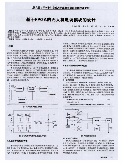
的 是I R 2 l 3 2 芯片 ,此 芯片 是 利用 电容 充放 电技 术 来驱 动 功 率MO S . F E T 设计 的, 由于 其 内部 驱动 器 的 导通 阻抗 小 , 因此在 MO S F E T 的 栅 极 以及源 极加 入 了 电阻 以保证 更好 的工 作 “ 。
含 了 电平 转 换 和 驱动 电路 等 简 单 电路 ,避 免 了MC U等 单指 令 周 期 芯 片 的时序 特 点 ,系 统硬 件结 构简 单 ,扩 展性 更 强 。能够 满足 各种 类型 无人 机 的实 时远 程控 制要 求 。 本 设计 系统 框 图如 图 l 所示 ,是 一个 闭环 反馈 系 统 ,控 制 量 是
图1无 人 机 电 调 模 块 原 理 图
巳
=  ̄l u F /=
l ∞V
图 2三 相 功 率 桥 电 路 以 及 位 置 检 测 电路
图3 PI D 控 制 器原 理 图
2 . 系 统硬 件 电 路 设 计 方 案
本 设 计 选 用 的 是 自带 数 字 型霍 尔 传 感 器 的无 刷 直 流 电机 , 电 极对 数 为 I , 可反 馈 三路 H a 、H b 、H c 霍尔 信 号 。额 定转 速 为3 0 0 0 r / mi n , 额 定 电压 为 2 4 V。硬 件 电路 部 分 包 括 功率 桥 电路 , 位置 检 测
的 无 人机 电调主 要 是 由单 片机 、A R M等 实现 的。采 用 基于 F P GA 设
计 无 人机 电调 ,充 分利 用 了F P G A并 行数 据 处理 能 力 和 同步 设 计优 势 ,将 大 部 分功 能 模块 都 集 成 在F P G A芯 片 内部 , 外 围 电路仅 仅 包
- 1、下载文档前请自行甄别文档内容的完整性,平台不提供额外的编辑、内容补充、找答案等附加服务。
- 2、"仅部分预览"的文档,不可在线预览部分如存在完整性等问题,可反馈申请退款(可完整预览的文档不适用该条件!)。
- 3、如文档侵犯您的权益,请联系客服反馈,我们会尽快为您处理(人工客服工作时间:9:00-18:30)。
I.J.Modern Education and Computer Science, 2012, 7, 24-30Published Online July 2012 in MECS (/)DOI: 10.5815/ijmecs.2012.07.04FPGA Based Pipelined Parallel Architecture forFuzzy Logic ControllerVinod KapseResearch Scholar, Dept. of Electronics & Communication Engg. Jabalpur Engineering College, Jabalpur, IndiaEmail: kapse.vinod@Bhavana JhariaAssociate Professor, Dept. of Electronics & Communication Engg. Jabalpur Engineering College, Jabalpur, IndiaEmail: dr.bhavana.jharia@S. S. ThakurProfessor, Dept. of Mathematics, Jabalpur Engineering College, Jabalpur, IndiaEmail: samajh_singh@Abstract— This paper presents a high-speed VLSI fuzzy inference processor for the real-time applications using trapezoid-shaped membership functions. Analysis shows that the matching degree between two trapezoid-shaped membership functions can be obtained without traversing all the elements in the universal disclosure set of all possible conditions. A FPGA based pipelined parallel VLSI architecture has been proposed to take advantage of this basic idea, implemented on CycloneII-EP2C70F896C8. The controller is capable of processing fuzzified input.The proposed controller is designed for 2-input 1-output with maximum clock rate is 12.96 MHz and 275.33 MHz for 16 and 8 rules respectively. Thus, the inference speed is 0.81 and 34.41 MFLIPS for 16 and 8 rules, respectively.Index Terms—VLSI, FPGA, Pipelined, Inference Processor, Matching Degree.I.I NTRODUCTIONFuzzy inference techniques [1] are becoming an attractive approach to solve control and decision-making problems. This is mainly due to its inherent ability to manage the intuitive and ambiguous behavioral rules given by a human operator to describe a complex system. The application of fuzzy technologies to real-time control problems implies that hardware realizations be adapted to the fuzzy paradigm. Many microelectronics implementations of fuzzy controllers have been proposed recently [2-7]. However, if fuzzy controllers are to be massively adopted in consumer products, they must fulfill some additional characteristics. First, they must be flexible, that is, suitable for adapting their functionality to different applications. This implies the capability to program the knowledge base and select different inference mechanisms. On the other hand, considering fuzzy controllers as integrated circuits, they must be efficient in terms of operational speed.Fuzzy Logic (FL) control system implemented and tested successfully on simple, small, embedded micro-controllers to large, networked, multi-channel PC or workstation-based data acquisition and control systems, but they are not precise to achieve more accurate control such type of controller should be implemented on FPGA which is faster and cost effective.The various fuzzy inference systems are realized by different researcher for different applications. The original digital realization of fuzzy inference processor was performed by Toga and Watanabe [2]. H. Peyravi et al. [6] have proposed reconfigurable inference engine for the analog fuzzy logic controller, based on Mamdani inference technique. J.M. Jou et al. [7], R. d 'Amore [8] and N. E. Evmorfopoulong et al. [9] have proposed different architecture for the fuzzy inference processor. Many variations [1-14] have been proposed to improve the inferencing performance. The speed bottleneck of these fuzzy inference processors lies in the calculation of the matching degree. In order to obtain the matching degree between two membership functions, these fuzzy inference processors need to traverse all the elements in the universal disclosure set. As a result, calculating the matching degree requires very high latency, which limits the overall circuit performance.Some digital hardware fuzzy inference processors [7-8] restrict their inputs to crisp values; in other words, they do not tackle fuzzified inputs. Since calculation of the matching degree requires a crisp value and a membership function, these fuzzy inference processors need not traverse all the elements in the universal disclosure set to obtain the same. The main drawback of these fuzzy inference processors [7-8] is that they do not cover the ignorance of the input measure.Figure 1. Block diagram of the Max-Min CalculatorAsica, Catania and Russo [12] assumed that each membership function is composed of nine segments. Based on this assumption, they used a binary search mechanism to obtain the matching degree between two membership functions. The main drawback of their fuzzy inference processor [13] is that they applied a detection process to extract active rules from the knowledge base. As a result, the inference speed of their fuzzy inference processor depends on the number of active rules. Therefore, their fuzzy inference processor is only suitable for applications that have few active rules.In this paper, it is assumed that each membership function is in trapezoid-shape. The matching degree between two trapezoid-shaped membership functions can be obtained by providing fuzzy input to the controller. Based on this analysis, a pipelined parallel FPGA based hardware is proposed to take advantage of basic idea. The rest of the paper is organized as follows. Section II present the motivation for fast calculation of the matching degree. The architecture of our proposed fuzzy inference processor is described in section III. Comparisons with other hardware architectures are presented in section IV. Finally, some concluding remarks are presented in section V.II.M IN-MAX UNITThe block diagram of the max min calculation is shown in fig.1. This block is used to calculate the degree of membership function. For this design, assuming that the membership grades are discretized into 16 levels which is represented by l=4 bits and it has 64 elements at universal disclosure i.e. e=6 bits. Thus the degree of membership ranges from 0 to 1 is represented as 0000 to 1111, respectively.The max-min block is used to calculate the matching degree of the fuzzy input and antecedent membership functions as shown in fig. 1. Assume that the trapezoidal antecedent membership function is (a1, a2, a3, and a4) and the trapezoidal fuzzified input is (x1, x2, x3, and x4). The following four mutually exclusive conditions are used to calculate the degree of matching between the antecedents and fuzzified input membership functions. The conditions are as follows: 1. If a3 < x2 and x1 < a4: MD is the grade value of the cross-over point ( Fig. 2).2. If x3 < a2 and a1 < x4: MD is the grade value of the cross-over point (Fig. 3).3. If a1=x1, a2=x2, a3=x3, a4=x4: MD = …1‟ (Fig. 4).4. If a4 ≤x1 or x4 ≤a1: MD = …0‟ (Fig. 5).Figure 2. Cross Over PointFigure 3. Cross Over PointFigure 4. Complete MatchingFigure 5. No MatchingThe max-min calculator circuit is consisting of comparator, multiplexers, subtractors, adders, divider and shifter circuit. The comparator circuit is used to differentiate four condition to find matching degree. The inputs to the comparator circuit are a1, a2, a3, a4, x1, x2, x3 and x4, whereas circuit produces two bit output to find out matching degree for four different condition that may occur. According to the result obtained by the comparator circuit, the output of the dedicated max-min calculation hardware is selected. The 00 and 11 output value of comparator circuit indicates that the two membership functions are completely matched or mismatched respectively. The value “01” output of the comparator circuit realizes the equation (1) and “10” realize s equation (2).If (a3 < x2 and x1 < a4) Then()( ) If (x3 < a2 and a1 < x4) Then()( )The proposed fuzzy controller has pipelined parallel architecture with 16 and 8 rules, two inputs and one output variable. The membership degree is divided into 16 levels which is represented by l=4 bits.III.PROPOSED ARCHITECTUREThe fuzzy inference execution can be split into the following three primary steps: fuzzy decoding, inference decision, and defuzzification. The proposed fuzzy decoding is a pipelined architecture is shown in fig. 6. The center of gravity (COG) technique is used for defuzzification process. This can be done using accumulation and division process.Figure 6. The Pipelined ArchitectureA.Fuzzy DecodingThe function of fuzzy decoding unit is to find the weights of rules, including weight0, weight1… weight16, as shown in fig.7. The function of the max-min calculator is split into two phases. Thus, the fuzzy decoding step is also divided into two pipeline stages.Two max-min calculation units operate in parallel to obtain the matching degrees of the two input variables at the same time, as shown in Eqs. (3) and (4).( ( ()())) ( )( ( ()())) ( ) Then, a minimum unit is employed to obtain the weight, as shown in equation (5).() ( ) Note that, at each pipeline stage, a rule will take only two clock cycles. Thus, in order to utilize the fuzzy decoder fully, four rules are processed sequentially during a pipeline stage. In the first pipeline stage, two 4-to-1 multiplexers are used to sequentially pass the rules to max-min calculators; in the second pipeline stage, a 1-to-4 demultiplexer is used to sequentially store the obtained weights. This fuzzy decoder is expandable. To process 16 rules, four fuzzy decoders, operating in parallel are employed. During a pipeline stage, rules R4i (i = 0, 1, 2, 3) are processed in the first and the second cycles, rules R4i+1 (i = 0, 1, 2, 3) are processed in the third and the fourth cycles, rules R4i+2 (i = 0, 1, 2, 3) are processed in the fifth and the sixth cycles, and so on.B.Inference DecisionThe inference decision unit finds degree of membership of the output variable, including O(0), O(1), …, and O(15). Each grade O(m), where m = 0, 1, 2, …, and 15, is determined by means of a maximum of 16 control decisions, which are O0(m), O1(m), …, and O16(m).Simultaneously operating, 16 control decision units are employed. As equation (6) shows, the control decision of a rule O i(m) is obtained by means of the minimum between weight i and C i(m), where m = 0, 1, 2, …, and 16, and i = 0, 1, 2, …, and 16.()(( )) ( )Fig. 8 depicts the control decision unit of a fuzzy rule. The weighti , which is the weight of rule Ri , is calculated in the fuzzy decoding step. Ci is the consequent membership function associated with rule Ri . For computation of Oi (m ), where m = 0, 1, 2, …, and 16, we need to have all 64 elements of . To find all the control decisions within a pipeline stage, four 4-to-1 multiplexers are used. Then, Ci (15), Ci (11), Ci (7), and Ci (3) are sampled on the first cycle, Ci (14), Ci (10), Ci (6), and Ci (2) are sampled on the second cycle, and so on. Consequently, Oi (15), Oi (11), Oi (7), and Oi (3) are obtained on the first cycle, Oi (14), Oi (10), Oi (6), and Oi (2) are obtained on the second cycle, and so on.Four maximum units, i.e., MAX1, MAX2, MAX3, and MAX4, are used to calculate output. The output is calculated using equation (7) is as follows:( ) ( ( ) ( )) ( )Each maximum unit has 64 inputs. In the first cycle, the inputs to MAX1 are ( ) ( ) ( ); the inputs to MAX2 are ( ) ( ) ( ), the inputs to MAX3 are O 0(11), O 1(11), …, and O 15(11); and the inputs to MAX4 are ( ) ( ) ( ). In the second cycle, the inputs to MAX1 are ( ) ( ) ( ) ( ); the inputs to MAX2 are ( ) ( ) ( ) ( );the inputs to MAX3 are ( ) ( ) ( ) ( ); the inputs to MAX4 are ( ) ( ) ( ) ( ); and so on.Figure7. Fuzzy decoder unitFigure 8. Fuzzy control decision unitC.DefuzzificationThe Center of gravity defuzzification method is used to find the final output. It includes two pipeline stages: accumulation and division. For processing the output, four parallel maximum units are used. The numerator N and denominator D is calculated using equation (8) and (9), respectively.∑()∑()∑()∑() ( )∑()∑()∑()∑() ( ) After calculating the value of N and D, the output will be calculated using N/D.PARISONSome high-speed fuzzy inference processors are proposed in [3, 5, 8, 10, 13] and [14] using different approaches such as ASIC, FPGA, DSP and MIPS processor approach.Note that the [10] is a software implementation running on a high-speed DSP, those in [5, 8] and [14] are FPGA implementations, and [13] is an extension of the MIPS processor. Table I shows the comparative study of proposed design with different architectures in terms of resolution , number of inputs and outputs, number of rules and speed in terms mega logic inferences (MFLIPS). Table I compares proposed fuzzy inference processor with above mentioned fuzzy inference processor concludes that it achieves very high performance. It is worth mentioning that [3] and [13] executed their instructions sequentially. Therefore, the works in [3] and [13] are only suitable for applications that have few rules or whose required inference speeds are not high.V.CONCLUSIONIn this paper, a high-speed VLSI fuzzy inference processor for the real-time applications using trapezoid-shaped membership functions has been presented. From the analysis it is clear that the matching degree between two trapezoid-shaped membership functions can be obtained without traversing all the elements in the universal disclosure set of all possible conditions. A pipelined parallel VLSI architecture has been proposed to take advantage of this basic idea.The proposed fuzzy inference processor has been implemented on FPGA CycloneII- EP2C70F896C8. The proposed controller is designed and found maximum clock rate as 12.96 MHz and 275.33 MHz for 16 and 8 rules respectively. Thus, the inference speed is 0.81 and 34.41 MFLIPS for 16 and 8 rules respectively.TABLE I COMPARATIVE STUDY OF DIFFERENT FUZZY CONTROLLERREFERENCES[1]K. Nakamura, N. Sakashita, Y. Nitta, K.Shimomura, and T. Tokuda, “Fuzzy inference andfuzzy inference processor,” IEEE Micro, Vol. 13,1993, pp. 37-48.[2]M. Togai and H. Watanabe, “Expert system on achip: an engine for real-time approximatereasoning ,”IEEE Expert Magazine, Vol. 1, 1986,pp. 55-62.[3]S.H.Huang et al, “High Speed Fuzzy Inferencep rocessor Using Active Rules Identification” JCIS06-Joint conference on Information Sciences, Oct 8-11, 2006, Taiwan.R. J. Dirkman and J.Leonard,68HC11 Microcontroller LaboratoryWorkbook, Prentice Hall, 1996.[4]J.Y. Lai et al, “A High Speed VLSI Fuzzy LogicController with Pipeline Architecture”, Proceedingsof IEEE International Conference on Fuzzy Systems, vol. 3, pp.1054-1057, 2001[5] F. Homburg and R. Palomera-Garcia, “A high-speed scalable and reconfigurable fuzzy controller,”in proceedings of IEEE International Symposium onCircuits and Systems, Vol. 5, 2003, pp. 797-800 [6]H. Peyravi, A. Khoei, and K. Hadidi, “Design of anan alog CMOS fuzzy logic controller chip”, FuzzySets and Systems 132, PP. 254-260, 2002.[7]J. M. Jou and P. Y. Chen, “An adaptive fuzzy logiccontroller: its VLSI architecture and applications,”IEEE Transactions on Very Large Scale Integration(VLSI) Systems, Vol. 8, 2000, pp. 52-60.[8]R. D‟Amore, O. Saotome, and K. H. Kienitz, “Atwo-input, one-output bit-scalable architecture forfuzzy processors,” IEEE Design and Test ofComputers, 2001, pp.56-64.[9]N. E. Evmorfopoulos, and J. N. Avaritsiots, “Anadaptive digital fuzzy architecture for application-specific integrated circuits”, Active and PassiveElec. Comp., Vol. 25, pp. 289-306, 2002.[10] E. Frias-Martinez, “Real-time fuzzy processor on aDSP,” in Proceedings of IEEE InternationalConference on Emerging Technologies andFactory Automation, Vol.1, 2001, pp. 403-408. [11]Sajad A. Loan and Asim M. Murshid,“A NovelFuzzy Inference Processor using Trapezoidal-Shaped Membership Function”Proceedings of theIEEE International Conference on Open Systems(ICOS2011), September 25 - 28, 2011, Langkawi,Malaysia.[12]G. Asica, V. Catania, M. Russo, and L. Vita, “Ruledriven VLSI fuzzy processor,” IEEE Micro, Vol.1996, pp. 62-74.[13]V. Salapura, “A fuzzy RISC processor”, IEEETransactions on Fuzzy Systems, Vol.8, 2000, pp.781-790.[14]Shabiul Islam, Mukter Zaman, Bakri Madon, andMasuri Othman (2008). Designing Fuzzy BasedMobile Robot Controller using VHDL. InternationalJournal of Mathematical Models and Methods inApplied Science, Issue 1, Volume 2, ,p-p 138-142.Vinod Kapse born at Nagpur in India. He received the B.E. degree in Industrial Electronics from Amaravati University, Amaravati , India, in 1998, M. Tech. degree in Electronics Engg. from Nagpur University, Nagpur , India in 2007.In 1999, he joined the Srijan Control Drives in R & D department. In 2000, he joined the Sibar Software Services (India) Ltd. as a Design Engineer. In 2002, he joined as a Lecturer in Department of Electronics & Communication in Guru Ramdas Khalsa Institute of Science & Technology, Jabalpur(M.P.) India. He has been member of IEEE. He is currently a Asst. Professor in Gyan Ganga Institute of Technology & Science,Jabalpur(M.P.) India. His research interest includes VLSI Design, Fuzzy logic, Robotics.Bhavana Jharia is presently working as a Associate professor in Department of Electronics & Communication Engineering, Jabalpur Engineering College, Jabalpur, (M. P.), INDIA. Dr. B. Jharia received B.E. degree from Government Engineering College, Jabalpur in 1987 , M.E. from UOR, Roorkee in 1998 and Ph. D. Degrees from I.I.T. Roorkee in 2008. She has published more than 40 research papers in national, International Journals and supervised 30 B.E. 20 M.E. thesis in the area of VLSI design, Communication etc. She is a member of IEEE, IE (I), CSI, VLSI Society of India, senior member of IACSIT and Life Member of ISTE. She has been the coordinator, National Mission on Education through ICT conducted by I.I.T. Bombay. She is a member of editorial board and reviewer of many International Journals and Conferences. The main interest of her current work includes VLSI Design, Communication, Wireless communication and Fuzzy Logic. S. S. Thakur is presently working as a professor in Department of Applied Mathematics and Coordinator Advanced Computing Centre of Fuzzy Technology, Jabalpur Engineering College, Jabalpur, (M. P.), INDIA. Dr. Thakur received M. Sc. and Ph. D. Degrees in mathematics from Dr. Hari Singh Gour University, Sagar in 1977 and 1982 respectively. He has published more than 160 research papers and supervised sixteen Ph. D. students most in the area of Topology and Fuzzy Topology and Fuzzy Data bases. He has been the organizing secretary of an International conference on “Soft Computing and Intelligent Systems” held in Dec. 2007. He is a member of editorial board and serves as referee of many international Journals. The main foci of his current work includes Intuitionist Fuzzy Topology and applications of Intuitionist Fuzzy Sets in Databases.。