FIN 350-06a_note
无线全双工对讲系统基站 FDI-BS 350 用户手册说明书

Wireless Full Duplex Intercom System Base Station FDI-BS350Users’Manual Please read the manual carefully before operationTable of ContentsChapter1Item List (3)Chapter2Preparations (3)Chapter3Indicators and Interfaces (4)Chapter4Interface Connection (5)4.1Headset Interface (5)4.2MIC Interface (5)4.3ANT Antenna Interface (5)4.4COM Port (5)4.5Tally Interface (6)4.6AUX IN (6)4.7AUX OUT (6)4.8Power Connection (7)Chapter5Basic Operations(Calling process) (7)5.1Introduction to Call Operation (7)5.2Call Selected Beltpacks (7)5.3Grouped Calling (8)5.4Base station Only Mode (8)5.5Setting Changes (8)Chapter6Optional Accessories (9)Chapter7Maintenance and Cleaning (10)Chapter8Quality Commitment and Maintenance Terms (11)Warranty Card (11)Chapter1Item listThe package contains the following items.If there is any damage or loss,please contact the dealer.Chapter2Preparations2.1InstallationThe FDI-BS350wireless intercom system and accessories could be installed in standard chassis,box,and cabinet.2.2AC Input Power RequirementsFDI-BS350consists of a switching power supply,The operating voltage of the deviceis AC110V/220V,it should be earthed correctly to ensure safety.2.3GroundedWell grounded is required,power plug has to be connected to a groundedreceptacle.Otherwise it may cause permanent damage to the device.Chapter 3Indicators and Interfaces3.1FrontPanel3.2Rear PanelChapter4Cable Connection&Interface4.1Headset ConnectorWhen the front panel Headset light is on,it means that the headset function is enabled,and the user is able to speak and listen.4.2MIC ConnectorWhen the front panel MIC light is on,it indicates that the gooseneck shapedmicrophone input function is enabled.The user is able to speak.4.3ANT Antenna InterfaceConnect the antenna to the ANT connector on the rear panel.Place the antenna correctly after installation.4.4COM PortThis port is to be connected with computer by a data configuration cable.You couldchange configurations,such as channel.It also supports tally signal input with RS232/RS485/RS422type.4.5Tally ConnectorConnect video switcher via dedicated Tally cable.This connector supports GPI type tally input.Pin1-12indicates PGM/red signal,pin14-25indicates PVW/green signal,pin13is GND.Dedicated tally data cable is required by certain brand and model/type of video switchers. It is recommended to use the corresponding tally data cable made by the manufacturer. When working with a different switcher,it is advised to confirm with the supplier about the tally date cable mode.Improper use of the data cable or incorrect connection may cause permanent damage to the device.4.6AUX IN3-pin cannon receptacle connector.The input level of the analog speech signal shall be1Vrms.4.7AUX OUT3-pin cannon connector.The input level of the analog speech signal shall be1Vrms.4.8Power ConnectionEach unit is attached with a power cable,which is used to connect AC110V/220V power supply with grounded receptacle.Chapter5Basic Operations(Calling process)5.1Introduction to call operationPress or button of base station,the lights are on.The base station could talk through headphone or microphone.Press again,the lights are off.The base station only receive audio signal.5.2Call Selected Belt-packsPress button,make sure the light is off.Now the number1to8indicates8 belt-packs.You could choose one or more belt-packs to speak with.5.2.1Belt-packs SelectedPress one or more digital keypad buttons of1-8on the base station,the button lights of the selected belt-packs are on.All selected belt-packs and base station could talk with each other.(Refer to Section 5.4)5.2.2Belt-pack UnselectedThe base station could turn off one or more of the digital keypad buttons1-8.The unselected belt-packs could send a voice signal request to base station,but cannot send or receive voice signals.The flashing light on the base station indicates that the corresponding belt-pack is on the call.5.3Group CallingIn a specific scenario,the belt-packs need to be divided into many groups according to the department.All belt-packs of a group could only talk internally without disturbing other groups.Push button,the1-8number buttons indicate8groups,and the device supports up to8groups.Push the button again to exit the group mode.5.3.1Groups SelectedBase stations could talk with one or more groups by turning on corresponding digital button lights.All belt-packs of selected groups could talk with base station and talk with each other in the same group,but could not talk with other which in different group.5.3.2Groups UnselectedBase stations could disable one or more groups by turning off corresponding digital button lights.An unselected group could talk internally but unable to talk with base station.5.4Isolated ModeIsolated mode could be enabled by turning on the button light.Now the belt-packs could not talk with each other except base station.5.5Change SettingsPress button down and hold for5seconds,and release it up,to enter theconfiguration mode.In configuration mode,Press button will switch to nextmenu,press button to change setting.The menu includes channel setting,background noise level,noise suppression level,reset all settings and exit configuration mode.After change you should restart the base station to load the new configurations.5.5.1Channel SettingThe base station includes90channels,press button to change channel asvoice hint.The setting will be saved while no continue operation within4seconds.5.5.2Background Noise LevelThe base station may transmit voice and background noise to belt-packs.Base station could suppress the background noise at a certain level.The default setting is level1.You could change the level by pressing the button.Notes that the default settings are well tested,if not necessary please do not change the setting. Otherwise the voice may be interrupted with wrong setting.5.5.3Noise Suppression LevelThe setting allows the base station to suppress a certain level of the background noise transmitted from the belt-packs if they are not speaking.The default setting is level5.(Suppress the noise lower than5%.The level is adjustable by clicking the setting button.Chapter6Optional Accessoriesvideo switcher.6Attenuator Sometimes some video switcher,vidicom,SDI cables,HDMI cable or mixer with bad EMI design,may be influenced by RF signal.You have to attach an attenuator to base station to compatible with them.While the working distance will be short.Chapter7Maintenance and CleaningPlease read the following contents carefully in order for smoothly operation,long service life,better daily maintenance and cleaning.Maintenance●Do not use hard material to puncture or scrape device.●Do not put device in hard corrosive environment that may damage circuits.●Do not break the antenna.Cleaning●Please wipe the dust on the device with clean dry towel or brush.●If the device is dirty,please clean with neutral detergent and non-woven fabric,do not use detergent,alcohol,spray and other chemical agents to avoid thedamage of the device.Make sure that the device is dry thoroughly before using.Chapter8Quality Commitment and Maintenance TermsWe promises warranty services for material and manufacturing process defect under normal operation since purchase date.1.Warranty Scope and Duration12months for the base station2.Warranty ClaimYou have to provide product warranty card or valid purchase invoice to apply repair.The product mark should be kept clean and intact during the warranty period.Warranty CardIn order to protect your benefits,please fill in the following table carefully and keep it properly as a evidence for maintenance.Dealer’s informationProduct model Date of saleDealer’s name Contact numberUser’s informationUser’s name Contact numberAddress E-mailNAYAWeChat SubscriptionNumberShanghai NAYA intelligenceCo.Ltd.。
03-heat-exchanger

3. Specify the Periodic Conditions
Boundary Conditions → Press “Periodic Conditions” tab.
a. Under the “Type”, select “Specify Mass Flow” b. Set the Mass Flow Rate and Upstream Bulk Temperature to 1.385 kg/s and 240K,
Prerequisites
This tutorial assumes that you have successfully completed the introductory training for the ANSYS FLUENT solver.
Problem Description
The compact heat exchanger for this problem consists of the staggered fins that enhance the heat transfer relative to a continuous- fin heat exchanger by promoting t h e turbulent mixing in the wake region behind each fin and taking advantage of the relatively high heat transfer coefficients as the boundary layers continuously re-form on the interrupted fins. A sketch of the geometry, with dimensions in mm, is shown in Figure 1. The geometry contains symmetry boundary conditions at the top and bottom planes.
安装短路电流等级-500 500f 509型接触器和起动器说明书
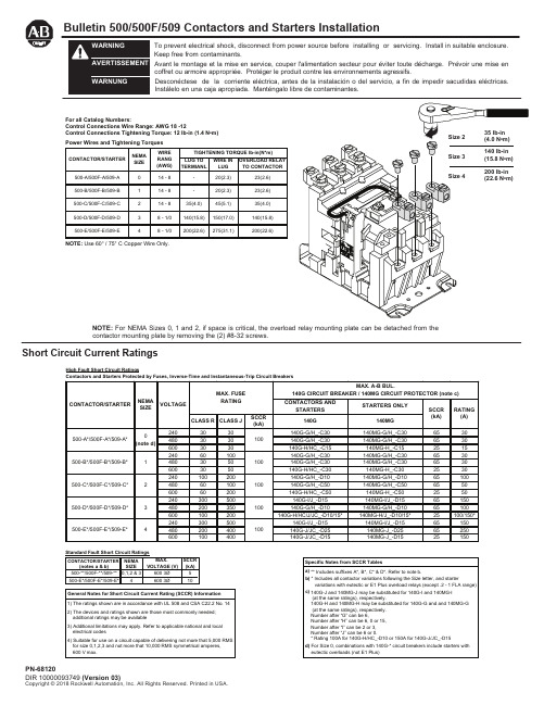
Bulletin 500/500F/509 Contactors and Starters InstallationShort Circuit Current RatingsTo prevent electrical shock, disconnect from power source before installing or servicing. Install in suitable enclosure. Keep free from contaminants.Avant le montage et la mise en service, couper l'alimentation secteur pour éviter toute décharge. Prévoir une mise encoffret ou armoire appropriée. Protéger le produit contre les environnements agressifs.Desconéctese de la corriente eléctrica, antes de la instalación o del servicio, a fin de impedir sacudidas eléctricas. Instálelo en una caja apropiada. Manténgalo libre de contaminantes.NOTE: For NEMA Sizes 0, 1 and 2, if space is critical, the overload relay mounting plate can be detached from the contactor mounting plate by removing the (2) #8-32 screws.High Fault Short Circuit RatingsFor all Catalog Numbers:Control Connections Wire Range: AWG 18 -12Control Connections Tightening Torque: 12 lb-in (1.4 N •m) NOTE: Use 60° / 75° C Copper Wire Only.Renewal Parts and Accessory KitsRenewal Contact Kit for Power Poles (One Pole Per Part No.)Size 0 ……………………………………………………….................................................Part No. 40410-331-51Size 1 ……………………………………………………….................................................Part No. 40410-331-52Size 2 ……………………………………………………….................................................Part No. 40420-322-51Size 3 ……………………………………………………….................................................Part No. 40430-300-51Size 4………………………………………………………..................................................Part No. 40440-300-51 Operating Coil…………...........................................................................................(Specify number and rating on coil label) Auxiliary ContactsSingle circuit (1 N.O.)……………………………………………………...…….........................Catalog No. 595-ASingle circuit (1 N.C.)………………………………………………...…….…….........................Catalog No. 595-BSingle circuit (1 N.C. Late Break) ………………..………………...……...............................Catalog No. 595-BLDouble circuit (2 N.O.)……………………………………………..…...……...........................Catalog No. 595-AADouble circuit (2 N.C.)……………………………………………..…………..........................Catalog No. 595-BBDouble circuit (1 N.O.-1 N.C.)……………………………………….....……….......................Catalog No. 595-AB Power Pole Adder KitSizes 0 and 1…………………………………………………………………..……...............Catalog No. 599-P01ASize 2………………………………………………………………………..….........................Catalog No. 599-P2ASize 3……………………………………………………………………........……...................Catalog No. 599-P3ASize 4……………………………………………………………………....………....................Catalog No. 599-P4ANOTE: Contactor sizes 0, 1 and 2 with 50 Hz coils and all size 3 and 4 contactors require a special coil(coil number ending with the letter “C”) whenever one or two power poles are added.Control Circuit Fusing KitSingle Pole, Rejection Fuse Only………………………………........................................Catalog No. 599-FR04NOTE: When contactor-mounted, each kit occupies the space of one double circuit auxiliary.Surge Suppressor12-120 Volt AC ...............………………………………………………....……..….................Catalog No. 599-K04240 Volt AC ................………………………………………..………..…….........................Catalog No. 599-KA04 Tie Point TerminalSizes 0, 1 and 2.....………………………………………………...……..….…....................Catalog No. 599-TP02Sizes 3 and 4……...……………………………………………...…………..….…................Catalog No. 599-TP34 Control Terminal KitSizes 0, 1 and 2 ..…………………………………………………...……..….…...................Catalog No. 599-CT02Size 3 .............……...……………………………………………...…………..….…...............Catalog No. 599-CT3Size 4 ............................................................................................................................. Catalog No. 599-CT4 Load Terminal Shield for Top Wired ContactorSizes 0, 1 and 2………………………………………………………………………………...Catalog No. 599-TS02Sizes 3 and 4..………………………………………………………………………...............Catalog No. 599-TS34 Top Wiring Terminal Kit (3 terminals)Sizes 0 and 1 ……………………………………………………….……..……….….........Catalog No. 599-TW01Size 2………………………………………………………………….…..……..…..................Catalog No. 599-TW2Size 3………………………………………………………………….……………..................Catalog No. 599-TW3Size 4………………………………………………………………….……....……..................Catalog No. 599-TW4 Timer Attachment KitLeft Hand On Delay……………………………………………...……....…….......................Catalog No. 596-TL32Left Hand Off Delay…………………………………………………..…...….........................Catalog No. 596-TL33Right Hand On Delay……………………………………………..……...….........................Catalog No. 596-TR32Right Hand Off Delay…………………………………………..……...................................Catalog No. 596-TR33NOTE: For size 2 contactors a special coil (coil number ending with the letter “C”) is required with any timer.When ordering specify catalog number and series letter on the device.Note: additional control circuit overcurrent protection may be required. refer to the National Electrical Code.The current rating of the control circuit conductors furnished with this device is 15 amperes for sizes 0 through 3 and 20 amperes for size 4.Maintain this equipment in accordance with guidelines of NFPA-70b, Electrical Equipment Maintenance.。
MAX9814中文资料ver2.0
```````````````````````````````````গၤNBY:925ဵጙࢅ߅۾Ăອᒠ൱యज़हࡍLjดᒙᔈࣅᐐፄ఼ᒜ)BHD*ጲૺࢅᐅဉ൱యज़ມᒙăকୈૹ߅ࢅᐅဉ༄ᒙहࡍĂభܤᐐፄहࡍ)WHB*Ăၒ߲हࡍĂ൱యज़ມኹखညጲૺBHD఼ᒜ࢟വăࢅᐅဉ༄ᒙहࡍࡼᐐፄৼࢾᆐ23eCLjऎWHBᐐፄభጲোၒ߲࢟ኹਜ਼BHDඡሢᏴ31eCਜ਼1eCᒄମᔈࣅࢯஂăၒ߲हࡍᎌ9eCĂ29eCਜ਼39eCྯᒬభኡᐐፄăᏴᎌኹჁࡼᄟୈሆLjहࡍೊభဧᔐᐐፄࡉࡵ51eCĂ61eC71eCăྯზၫᔊၒྜྷܠ߈ᒙၒ߲हࡍࡼᐐፄăᅪݝ࢟ᔜॊኹ఼ᒜBHDඡሢLjৈ࢟ྏభᒙࣅ0ျहဟମăྯზၫᔊၒྜྷથభܠ߈ᒙࣅᎧျहဟମࡼ܈LjBHDࡼۣߒဟମৼࢾᒋᆐ41ntăࢅᐅဉ൱యज़ມᒙखညถᆐࡍࣶၫᓘᄏ൱యज़ᄋມኹăNBY:925ݧஂဏహମࡼ25୭UEGOॖᓤăকୈਖࢾᔫᏴ.51°Dᒗ,96°D౫ᐱᆨࣞपᆍă```````````````````````````````````።```````````````````````````````````ᄂቶ♦ᔈࣅᐐፄ఼ᒜ)BHD*♦ྯᒬᐐፄᒙ)51eCĂ61eCĂ71eC*♦భܠ߈ࣅဟମ♦భܠ߈ࣅᎧျह܈♦3/8Wᒗ6/6W࢟Ꮞ࢟ኹपᆍ♦ࢅࡉ41oW0√I{ࡼၒྜྷݬఠᐅဉමࣞ♦ࢅࡉ1/15&!)࢜ቯᒋ*ࡼUIE ♦ࢅਈࣥෝါ♦ดݝᄋࢅᐅဉ൱యज़ມᒙLj3W♦ݧஂဏహମࡼ25୭UEGO!)4nn!y!4nn*ॖᓤ♦.51°Dᒗ,96°D౫ᐱᆨࣞपᆍNBY:925ᎌBHDਜ਼ࢅᐅဉ൱యज़ມᒙ࢟വࡼ൱యज़हࡍ________________________________________________________________Maxim Integrated Products 1```````````````````````````````ࢾ৪ቧᇦ`````````````````````````````````````````````````````````````````````````````````଼છౖᅄ۾ᆪဵ፞ᆪၫᓾ೯ࡼፉᆪLjᆪᒦభถࡀᏴडፉࡼݙᓰཀྵࡇᇙăྙኊጙݛཀྵཱྀLj༿Ᏼิࡼଐᒦݬఠ፞ᆪᓾ೯ăᎌਈଥৃĂૡૺࢿ৪ቧᇦLj༿ೊNbyjnᒴሾ၉ᒦቦǖ21911!963!235:!)۱ᒦਪཌ*Lj21911!263!235:!)ฉᒦਪཌ*LjषᆰNbyjnࡼᒦᆪᆀᐶǖdijob/nbyjn.jd/dpnă+ܭာᇄ)Qc*0९SpITܪᓰࡼॖᓤăU!>!௳ࡒ۞ᓤă*FQ!>!ൡă୭ᒙᏴၫᓾ೯ࡼᔢઁ߲ăၫ൩ሤ૦ၫᔊስ૦QEB ౸ዀऐ૦Ꭵಘᇹᄻ)ಿྙLjఌ౯PL*ၷሶᄰቧᓤᒙອᒠܣቑါഺስ૦JQ࢟જ0࢟જ્ፇN B Y :925ᎌBHDਜ਼ࢅᐅဉ൱యज़ມᒙ࢟വࡼ൱యज़हࡍABSOLUTE MAXIMUM RATINGSELECTRICAL CHARACTERISTICS(V DD = 3.3V, SHDN = V DD , C CT = 470nF, C CG = 2μF, GAIN = V DD , T A = T MIN to T MAX , unless otherwise specified. Typical values are at T A = +25°C.) (Note 1)Stresses beyond those listed under “Absolute Maximum Ratings” may cause permanent damage to the device. These are stress ratings only, and functional operation of the device at these or any other conditions beyond those indicated in the operational sections of the specifications is not implied. Exposure to absolute maximum rating conditions for extended periods may affect device reliability.V DD to GND..............................................................-0.3V to +6V All Other Pins to GND.................................-0.3V to (V DD + 0.3V)Output Short-Circuit Duration.....................................Continuous Continuous Current (MICOUT, MICBIAS).......................±100mA All Other Pins....................................................................±20mAContinuous Power Dissipation (T A = +70°C)14-Pin TDFN-EP(derate 16.7mW/°C above +70°C)........................1481.5mW Operating Temperature Range ...........................-40°C to +85°C Junction Temperature......................................................+150°C Lead Temperature (soldering, 10s).................................+300°C Bump Temperature (soldering) Reflow............................+235°CNBY:925ᎌBHDਜ਼ࢅᐅဉ൱యज़ມᒙ࢟വࡼ൱యज़हࡍ_______________________________________________________________________________________3Note 1:Devices are production tested at T A = +25°C. Limits over temperature are guaranteed by design.Note 2:Dynamic range is calculated using the EIAJ method. The input is applied at -60dBFS (0.707μV RMS ), f IN = 1kHz.Note 3:Attack time measured as time from AGC trigger to gain reaching 90% of its final value.Note 4:CG is connected to an external DC voltage source, and adjusted until V MICOUT = 1.23V.Note 5:CG connected to GND with 2.2μF.ELECTRICAL CHARACTERISTICS (continued)(V DD = 3.3V, SHDN = V DD , C CT = 470nF, C CG = 2μF, GAIN = V DD , T A = T MIN to T MAX , unless otherwise specified. Typical values are at T = +25°C.) (Note 1)N B Y :925ᎌBHDਜ਼ࢅᐅဉ൱యज़ມᒙ࢟വࡼ൱యज़हࡍ4_______________________________________________________________________________________```````````````````````````````````````````````````````````````````````࢜ቯᔫᄂቶ(V DD = 5V, C CT = 470nF, C CG = 2.2μF, V TH = V MICBIAS x 0.4, GAIN = V DD (40dB), AGC disabled, no load, R L = 10k Ω, C OUT = 1μF,T A = +25°C, unless otherwise noted.)GAIN vs. FREQUENCYFREQUENCY (Hz)G A I N (d B )10k1k 1001020304050607080010100kPOWER-SUPPLY REJECTION RATIOvs. FREQUENCYFREQUENCY (Hz)P S R R (d B )10k1k 100-70-60-50-40-30-20-100-8010100kMICBIAS POWER-SUPPLY REJECTION RATIOvs. FREQUENCYFREQUENCY (Hz)P S R R (d B )10k1k 100-100-90-80-70-60-50-40-30-11010100kSUPPLY CURRENT vs. SUPPLY VOLTAGEM A X 9814 t o c 04SUPPLY VOLTAGE (V)S U P P L Y C U R R E N T (m A )5.55.04.04.53.53.02.62.72.82.93.03.13.23.33.43.52.52.56.0SHUTDOWN CURRENT vs. SUPPLY VOLTAGEM A X 9814 t o c 05SUPPLY VOLTAGE (V)S H U T D O W N C U R R E N T (n A )5.55.04.54.03.53.00.10.20.30.40.502.56.0MICROPHONE BIAS VOLTAGEvs. MICROPHONE BIAS SOURCE CURRENTM A X 9814 t o c 06I MICBIAS (mA)V M I C B I A S V O L T A G E (V )2520151050.51.01.52.02.50030TOTAL HARMONIC DISTORTION PLUS NOISEvs. FREQUENCYFREQUENCY (Hz)T H D +N (%)10k1k 1000.11100.0110100kTOTAL HARMONIC DISTORTION PLUS NOISEvs. OUTPUT VOLTAGEOUTPUT VOLTAGE (V RMS )T H D +N (%)1.00.50.11100.011.5INPUT-REFERRED NOISEvs. FREQUENCYFREQUENCY (kHz)I N P U T -R E F E R R E D N O I S E (μV R M S /√H z )1010.1100100.0110010001NBY:925ᎌBHDਜ਼ࢅᐅဉ൱యज़ມᒙ࢟വࡼ൱యज़हࡍ_______________________________________________________________________________________5MICBIAS NOISE vs. FREQUENCYMA X 9814 t o c 10FREQUENCY (Hz)M I C B I A S N O I S E(n V RM S /√H z )10k1k 100100100010,0001010100kSMALL-SIGNAL PULSE RESPONSE200μs/divV MICIN 10mV/div0VV MICOUT500mV/div0VTURN-ON RESPONSEM A X 9814 t o c 1220ms/divV SHDN 5V/div 0V V MICBIAS 2V/div 0VV MICOUT 1V/div 0VV OUT vs. V INV IN (mV RMS )V O U T (V R M S)100500.250.500.751.0000150V OUT vs. V INV IN (mV RMS )V O U T (V R M S)3020100.250.500.751.000040V OUT vs. V INV IN (mV RMS )V O U T (V R M S )1050.250.500.751.000015ATTACK TIME200μs/divV MICOUT 500mV/divC CT = 47nF0VATTACK TIME200μs/divV MICOUT 500mV/div0VHOLD AND RELEASE TIME20ms/divV MICOUT 500mV/divC CT = 47nF A/R = GND0V``````````````````````````````````````````````````````````````````````࢜ቯᔫᄂቶ)ኚ*(V DD = 5V, C CT = 470nF, C CG = 2.2μF, V TH = V MICBIAS x 0.4, GAIN = V DD (40dB), AGC disabled, no load, R L = 10k Ω, C OUT = 1μF,T A = +25°C, unless otherwise noted.)N B Y :925ᎌBHDਜ਼ࢅᐅဉ൱యज़ມᒙ࢟വࡼ൱యज़हࡍ6_______________________________________________________________________________________HOLD AND RELEASE TIME40ms/divV MICOUT 500mV/div0VHOLD AND RELEASE TIME100ms/divV MICOUT 500mV/div0V```````````````````````````````````````````````````````````````````````````````୭ႁී``````````````````````````````````````````````````````````````````````࢜ቯᔫᄂቶ)ኚ*(V DD = 5V, C CT = 470nF, C CG = 2.2μF, V TH = V MICBIAS x 0.4, GAIN = V DD (40dB), AGC disabled, no load, R L = 10k Ω, C OUT = 1μF,T A = +25°C, unless otherwise noted.)NBY:925ᎌBHDਜ਼ࢅᐅဉ൱యज़ມᒙ࢟വࡼ൱యज़हࡍ_______________________________________________________________________________________7MAX9814 AGC DISABLED400μs/div V MICIN 100mV/divV MICOUT(AC-COUPLED)1V/divMAX9814 fig01aMAX9814 AGC ENABLED400μs/divV MICIN 100mV/divV MICOUT(AC-COUPLED)1V/divMAX9814 fig01b0V0V0V0V```````````````````````````````ሮᇼႁීNBY:925ဵጙࢅ߅۾Ăອᒠ൱యज़हࡍLjดᒙᔈࣅᐐፄ఼ᒜ)BHD*ጲૺࢅᐅဉ൱యज़ມᒙăNBY:925ဵᎅࢅᐅဉ༄ᒙहࡍĂభܤᐐፄहࡍ)WHB*Ăၒ߲हࡍĂ൱యज़ມᒙखညጲૺBHD఼ᒜ࢟വࢀࣶৈݙᄴ࢟വᔝ߅ăดݝ൱యज़ມᒙखညᄋ3WࡼມኹLjး᎖ࡍࣶၫᓘᄏ࢟ྏါ൱యज़ăNBY:925ॊᆐྯLj࣪ၒྜྷቲहࡍăᏴጙLjၒྜྷᄰਭᐐፄᆐ23eCࡼࢅᐅဉ༄ᒙहࡍቲદߡਜ਼हࡍǗऔᐌᎅBHD఼ᒜࡼWHBᔝ߅LjWHB0BHDᔝถ৫ဧᐐፄᏴ31eCᎧ1eCᒄମܤછǗၒ߲हࡍဵᔢઁጙLjᎌ9eCĂ29eCĂ31eCྯৈݙᄴࡼৼࢾᐐፄLjభᄰਭጙৈྯზ൝ၒྜྷܠ߈ᒙăBHDᇄኹჁဟLjNBY:925ถ৫ᄋ51eCĂ61eC71eCࡼᐐፄăᔈࣅᐐፄ఼ᒜ)BHD*ݙ۸BHDࡼୈᏴၒྜྷᐐፄਭࡍဟLjၒ્߲߲ሚሻ݆ǗऎᏴၒྜྷᐐፄਭࡍဟLjBHDถ৫ܜၒ߲ሻ݆ăᅄ2Ⴥာᆐᐐፄਭࡍࡼ൱యज़ၒྜྷᏴᎌBHDਜ਼ݙࡒBHDࡼ༽ౚሆࡼ܈୷ăNBY:925ࡼBHD࣪ᐐፄቲ఼ᒜLj၅ሌଶހၒ߲࢟ኹဵ॥ިਭᎾඡሢăႲઁLjᄰਭభኡࡼဟମޟၫଢ଼ࢅ൱యज़हࡍᐐፄLjጲኀᑵਭࡍࡼၒ߲࢟ኹ७ᒋăᑚጙਭ߈߂ᆐࣅဟମăࡩၒ߲ቧ७ᒋଢ଼ࢅઁLjᐐፄᏴ੪ဟମดۣߒၱିᓨზLjႲઁၒ߲ቧદൻᐐଝࡵᑵޟᒋăকਭ߈߂ᆐۣߒਜ਼ျहဟମăहࡍࢯஂၒྜྷቧࡼႥࣞᎅᅪݝࢾဟ࢟ྏD DU ਜ਼B0S࣡࢟ኹᒙăBHDඡሢభᄰਭW UI ࢯஂăᐐፄၱିᆐၒྜྷቧ७ᒋࡼၫLjᔢࡍBHDၱିᆐ31eCăᅄ3߲೫ၒྜྷᅃި߲ᎾඡሢဟLj࣪ၒ߲ࣅဟମĂۣߒဟମਜ਼ျहဟମࡼ፬ሰăྙਫᒙࡼࣅဟମਜ਼ျहဟମሰ።ვLjᐐፄႲቧࣅზܤછऎႥࢯஂLjޟޟ્ޘညಢ႒Đກđဉ)qvnqjoh*Đࠇᇦđဉ)csfbuijoh*ࡼፒຫᐅဉăࢯஂBHDࡼဟମޟၫဧᎧဉᏎປLj࠭ऎࡉࡵᔢଛਫă࣪᎖กቋጲDEፒಘᆐᓍገፒᏎࡼ።ႁLjᅎୀࣅဟମᆐ271μtLjျहဟମᆐ91ntăᄰޟ༽ౚሆLjፒಘ݃ह۸ገ܈Ꭻፒ࢟፬ࢀ۸ኊገৎࡼျहဟମăᅄ2/!ࡒᎌBHDਜ਼ᎌBHDࡼ൱యज़ၒྜྷࣅဟମࣅဟମဵᒎࡩၒྜྷቧިਭඡሢ࢟ຳઁLjBHDଢ଼ࢅᐐፄჅኊࡼဟମăᐐፄᏴࣅဟମดጲᒎၫተါၱିLjࢾፃᆐጙৈဟମޟၫăকဟମޟၫᆐ3511y D DU )ᒦD DU ဵᅪݝࢾဟ࢟ྏ*ǖ•ኡན୷ࡼࣅဟମLjጲۣᑺBHDႥሰ።ၾზቧLjಿྙૣ৴ဉ)ፒಘ*།ૣဉ)EWE*ă•ኡ୷ޠࡼࣅဟମLjBHDၾဟख़ᒋLjᒑᎌࡩဉሰීመᐐଝဟݣଢ଼ࢅᐐፄăၾဟख़ᒋ݀ݙۻၱିLjࡣ୷ሰࡼဉፒۻၱିăᑚዹభ࠭ፒଢ଼ࢅሰဉLjဧࣅზपᆍᔢࡍછăۣߒဟମۣߒဟମဵᒎቧଢ଼ࡵඡሢጲሆĂျहਭ߈ఎဪጲ༄ࡼዓߕăۣߒဟମดݝᒙᆐ41ntLj݀༦ݙభࢯăࡩቧިਭඡሢLjᒮቤྜྷࣅࣤဟLjۣߒဟମᒫᒏăျहဟମျहဟମဵᒎቧࢰൢᒗඡሢጲሆLj݀༦ளਭ41ntࡼۣߒဟମᒄઁLjᐐፄૄࡵᑵޟၺຳჅኊࡼဟମăျहဟମࢾፃᆐࡩၒྜྷቧࢰൢᒗUIඡሢጲሆLj݀༦ளਭ41nt ࡼۣߒဟମᒄઁLjᐐፄ࠭31eCኹჁျहࡵᑵޟᐐፄࡼ21&ࡼဟମăျहဟମభࢯLjᔢቃᒋᆐ36ntăျहဟମᎅD DU ᒙࡼࣅဟମጲૺಽB0S )ྙܭ2Ⴥာ*ᒙࡼࣅ0ျहဟମ܈ཀྵࢾǖ•ݧቃ܈ᒋLjဧBHDࡼႥࣞࡉࡵᔢࡍă•ݧࡍ܈ᒋLjဧፒᒠࡉࡵᔢଛLjऴᒏBHDᒮআࢯஂဟମดި߲ඡሢࡼቧăBHDၒ߲ඡሢ૮BHDᔫࡼၒ߲ඡሢభᄰਭᅪݝ࢟ᔜॊኹࢯஂăᅲ߅࣪ॊኹࡼᒙઁLjBHDଢ଼ࢅᐐፄLjဧၒ߲࢟ኹᎧUIၒྜྷ࣡ᒙࡼ࢟ኹሤປă൱యज़ມᒙNBY:925ᎅดݝᄋࢅᐅဉ൱యज़ມᒙ࢟ኹLjభདࣅࡍࣶၫᓘᄏ࢟ྏါ൱యज़ăࢯஂ൱యज़ມᒙᒗ3WLjጲۣᑺྜྷࢅᐅဉ༄ᒙहࡍࡼၒྜྷቧݙۻὥᆡࡵă```````````````````````````````።ቧᇦᒙࣅဟମਜ਼ျहဟମࣅဟମਜ਼ျहဟମॊܰᎅDUਜ਼HOEᒄମࡼ࢟ྏጲૺB0Sࡼ൝ᓨზ)ܭ2*ࢾăB0Sᆐྯზ൝ၒྜྷLjభᒙࣅᎧျहဟମ܈ăোܭ3Ⴥࡼሤ።࢟ྏLjభጲኡᐋࣅဟମਜ਼ျहဟମăN B Y :925ᎌBHDਜ਼ࢅᐅဉ൱యज़ມᒙ࢟വࡼ൱యज़हࡍ8_______________________________________________________________________________________10ms/divATTACKRELEASEHOLDᅄ3/!ၒྜྷᅃިਭBHDඡሢܭ2/!ࣅᎧျह܈ܭ3/!ࣅ.ျहဟମᒙBHDඡሢྦገᒙ൱యज़ၒ߲ὥᆡဟࡼၒ߲࢟ኹඡሢLj።ᏴNJDCJBTਜ਼ᒄମೌᅪݝ࢟ᔜॊኹLj࢟ᔜॊኹၒ߲ೌࡵUIă࢟ኹW UIభཀྵࢾၒ߲ὥᆡဟࡼख़ᒋ࢟ኹඡሢăࠥဟLjၒ߲࣡ࡼᔢࡍቧڼ७ᆐW UIࡼ3۶Ljۣ݀ߒݙܤLjᒇࡵၒྜྷቧ७ᒋၱିᆐᒏăྦገணᒏBHDLjభUIೌᒗNJDCJBTă൱యज़ມᒙ࢟ᔜNJDCJBTభᏎ߲31nBࡼ࢟ഗăኡᐋးࡩࡼS NJDCJBTLj࠭ऎᆐᓘᄏ൱యज़ᄋჅኊገࡼມᒙ࢟ഗăጙۅႁLj3/3lΩࡼᔜᒋ࣪᎖࢜ቯഉැࣞࡼ൱యज़ጯளᔗ৫೫ăਈ᎖ມᒙ࢟ᔜࡼኡᐋLj༿ݬఠ൱యज़ၫᓾ೯ăມᒙ࢟ྏNBY:925ࡼCJBTၒ߲ᏴดݝளਭદߡLjᄋࢅᐅဉມኹăݧጙᒑ581oGࡼ࢟ྏCJBTവᒗăၒྜྷ࢟ྏ൱యज़हࡍࡼၒྜྷୣഗẮ࢟ྏ)D JO*ਜ਼ၒྜྷᔜఝ)S JO*ᔝ߅೫ጙৈᄰ݆Ljభ߹ၒྜྷቧᒦࡼჅᎌᒇഗມᒙ)ݬ࢜ቯ።࢟വ0ถౖᅄ*ăD JOభऴᒏၒྜྷቧᏎࡼᒇഗ߅ॊ߲ሚᏴहࡍࡼၒ߲ăଣၒྜྷቧᏎᔜఝᆐഃLjᐌᄰ݆ࡼ.4eC࢛ᆐǖኡᐋးࡩࡼD JOဧg.4eC`JOᏐࢅ᎖ැঢຫൈăg.4eC`JOᒙਭLj્፬ሰहࡍࡼࢅຫሰ።Ljኡᐋࢅ࢟ኹᇹၫࡼ࢟ᒠ࢟ྏă࣪᎖ୣഗẮ࢟ྏႁLjി࢟ஊ࢟ྏĂᶉ࢟ྏۡෞ࢟ᒠ࢟ྏ࣒ဵ੪ੑࡼኡᐋă࢟ኹᇹၫࡼ࢟ྏLjᓄྙჿࠣ࢟ྏ)ऻD1H࢟ᒠ*Lj્ଝ௭ࢅຫပᑞăၒ߲࢟ྏNBY:925ࡼၒ߲ມᒙᏴ2/34WLjྦገሿ߹ᒇഗပࢯLj።ݧୣഗẮ࢟ྏ)D PVU*ăఠࡵሆጙࡼၒྜྷᔜఝ)S M*LjD PVUਜ਼S Mᔝ߅ᄰ݆ăଣၒ߲ᔜఝᆐഃLjᄰ݆ࡼ.4eC࢛ᆐǖਈࣥNBY:925ᎌࢅਈࣥෝါăࡩSHDNᆐࢅ࢟ຳဟLj࢟Ꮞ࢟ഗࢰൢᒗ1/12μBLjၒ߲ྜྷᔜᓨზLj൱యज़ࡼມᒙ࢟ഗਈࣥăདࣅSHDNᆐ࢟ຳLjဧถहࡍă༿ᇖSHDNኞహă࢟ᏎവᎧQDCݚݧጙᒑ1/2μGࡼ࢟ྏ࢟ᏎവᒗăჁሣޠࣞభଢ଼ࢅည࢟ྏLjᅪݝᏄୈ።భถణதୈहᒙLjᅎୀኡܭᄣᏄୈăᏴᄴဟᎌෝผਜ਼ၫᔊࡼᇹᄻᒦLjNBY:925ࡼᎧෝผሤೌăNBY:925ᎌBHDਜ਼ࢅᐅဉ൱యज़ມᒙ࢟വࡼ൱యज़हࡍ_______________________________________________________________________________________9N B Y :925ᎌBHDਜ਼ࢅᐅဉ൱యज़ມᒙ࢟വࡼ൱యज़हࡍ10______________________________________________________________________________________```````````````````````````````````````````````````````````````````࢜ቯ።࢟വ0ถౖᅄNBY:925൱యज़हࡍ______________________________________________________________________________________11`````````````````````````````````በຢቧᇦPROCESS: BiCMOS`````````````````````````````````୭ᒙN B Y :925൱యज़हࡍ12______________________________________________________________________________________`````````````````````````````````````````````````````````````````````````````ॖᓤቧᇦྙኊᔢதࡼॖᓤᅪተቧᇦਜ਼ݚLj༿އኯ/packages ăNBY:925൱యज़हࡍ______________________________________________________________________________________13````````````````````````````````````````````````````````````````````````````````ॖᓤቧᇦ)ኚ*ྙኊᔢதࡼॖᓤᅪተቧᇦਜ਼ݚLj༿އኯ/packages ăN B Y :925൱యज़हࡍ````````````````````````````````````````````````````````````````````````````ኀࢿ಼ဥNbyjnݙ࣪Nbyjnޘອጲᅪࡼྀੜ࢟വဧঌᐊLjጐݙᄋᓜಽభăNbyjnۣഔᏴྀੜဟମĂᎌྀੜᄰۨࡼ༄ᄋሆኀখޘອᓾ೯ਜ਼ਖৃࡼཚಽă14____________________Maxim Integrated Products, 120 San Gabriel Drive, Sunnyvale, CA 94086 408-737-7600©2009 Maxim Integrated ProductsNbyjn ဵNbyjn!Joufhsbufe!Qspevdut-!Jod/ࡼᓖݿܪăNbyjn ۱யێူࠀ۱ய9439ቧረᎆᑶܠ൩211194ॅ࢟જǖ911!921!1421࢟જǖ121.732262::ࠅᑞǖ121.732263::。
i.MX6UL产品说明书
Product Features1.NXP i.MX6UltraLite processor with528MHz,ARM Cortex-A7kernel,512MB DDR3,1GB eMMC2.Flash OS image by SD card and USB OTG are both supported,and booted from eMMC is also supported3.Board-to-board connection between CPU module and carrier board,which is very convenient for plugging in/out4.Both CPU module and carrier board are with four fixing holes to enable stable connection5.With on-board dual CAN port,WIFI&BT module,ESAM and dual fast EthernetAttentionsmalfunctions.Please do not modify the product by yourself or use fittings unauthorized by us.Otherwise, the damage caused by that will be on your part and not included in guarantee terms.Any questions please feel free to contact Forlinx Technical Service Department..Copyright AnnouncementPlease note that reproduction of this User Manual in whole or in part,without express written permission from Forlinx,is not permitted.Updating RecordTechnical Support and Innovation1.Technical Support1.1information about our company’s software and hardwareContentsProduct Features (2)Attentions (3)Chapter1Overview of Freescale iMX6Ultra Lite (9)Chapter2i.MX6UL CPU Module Introduction (12)2.1CPU Module Overview (12)2.2FETMX6UL CPU Module Dimension (13)2.2CPU Module Features (13)2.3Power Supply Mode (14)2.4Working Environment (14)2.5CPU Module Interface (14)2.6CPU Module Pin Definition (15)2.6.1CPU module schematic (15)2.6.2CPU Module FETMX6UL-C Pin Definition (16)2.7CPU Module Design (21)Chapter3i.MX6UR Development Platform Overview (23)3.1Overview of single board computer i.MX6UR (23)3.2Carrier Board Dimension (24)3.3Base board resource: (24)3.4i.MX6UR Base Board Introduction (25)3.4.1Base Board Power (25)3.4.2Power Switch (25)3.4.3Reset Key (25)3.4.4Boot Configuration (26)3.4.5Serial Port(Debug Port) (27)3.4.6General Serial Port (28)3.4.7CAN (28)3.4.8SD Card Slot (28)3.4.9SDIO Port (29)3.4.10RTC Battery (29)3.4.11WIFI/Bluetooth (30)3.4.12Digital Camera Interface (30)3.4.13ESAM Interface (31)3.4.14RED (31)3.4.15Audio (31)3.4.16Dual Hundred Ethernet Ports (33)3.4.17USB Host (33)3.4.18JTAG Debug Port (34)3.4.19RCD Connector (35)3.4.20USB OTG (36)3.4.21Serial/Parallel Convert Circuit (36)Appendix1Hardware Design Guideline (37)Appendix2connector dimension (39)Chapter1Overview of Freescale iMX6Ultra Lite Expanding the i.MX6series,the i.MX6UltraLite is a high performance,ultra-efficient processor family featuring an advanced implementation of a single ARM®Cortex®-A7core,which operates at speeds up to528MHz.The i.MX6UltraLite applications processor includes an integrated power management module that reduces the complexity of external power supply and simplifies power sequencing.Each processor in this family provides various memory interfaces,including16-bit LPDDR2,DDR3,DDR3L, raw and managed NAND flash,NOR flash,eMMC,Quad SPI and a wide range of other interfaces for connecting peripherals such as WLAN,Bluetooth™,GPS,displays and camera sensors.Freescale i.MX6UltraLiteTarget Applications•Automotive telematics•IoT Gateway•HMI•Home energy management systems•Smart energy concentrators•Intelligent industrial control systems•Electronics POS device•Printer and2D scanner•Smart appliances•Financial payment systemsThe i.MX6UltraLite applications processor includes an integrated power management module that reduces the complexity of external power supply and simplifies power sequencing.Each processor in this family provides various memory interfaces,including16-bit LPDDR2,DDR3,DDR3L,raw and managed NAND flash,NOR flash,eMMC,Quad SPI and a wide range of other interfaces for connecting peripherals such as WLAN,Bluetooth®,GPS,displays and camera sensors.The i.MX6UltraLite is supported by discrete component power circuitry.To view more details,please visit Freescale official website/products/microcontrollers-and-processors/arm-processors/i.mx-applications-proces sors-based-on-arm-cores/i.mx-6-processors/i.mx6qp/i.mx-6ultralite-processor-low-power-secure-arm-co rtex-a7-core:i.MX6UL?uc=true&lang_cd=enChapter2i.MX6UL CPU Module Introduction 2.1CPU Module OverviewNAND Flash versionEMMC Version2.2FETMX6UL CPU Module DimensionDimension:40mm x50mm,tolerance±0.15mmCraftwork:thickness:1.15mm,6-layer PCBConnectors:2x0.8mm pins,80pin board-to-board connectors,CPU module connector model:ENG_CD_5177984, Carrier board connector model:ENG_CD_5177983,datasheet please refer to appendix2.2CPU Module FeaturesUnitUART Each up to5.0MbpseCSPI Full duplex enhanced sync.Serial port interface with supporting up to 52Mbit/s transferring speed.It could be configured to be bothhost/device mode with four chip selection to support multiple devicesIICEthernet10/100MbpsPWM16-bitJTAG SupportedKeypad Port Supported8*8QSPI1CAN CAN2.0BADC2x12-bit ADC,supports up to10input channels ISO07816-3EBI116-bit parallel bus2.6CPU Module Pin Definition2.6.1CPU module schematic2.6.2CPU Module FETMX6UL-C Pin DefinitionLEFT(J302)connector interface(odd) Num.Ball Signal GPIO Vol Spec.FunctionL_1G13UART5_RXD gpio1.IO[31] 3.3V UART5receiving IIC2_SDAL_3F17UART5_TXD gpio1.IO[30] 3.3V UART5sending IIC2_SCLL_5G16UART4_RXD gpio1.IO[29] 3.3V UART4receiving IIC1_SDAL_7G17UART4_TXD gpio1.IO[28] 3.3V UART4sending IIC1_SCLL_9H15UART3_CTS gpio1.IO[26] 3.3V UART3clear to send CAN1_TXL_11G14UART3_RTS gpio1.IO[27] 3.3V UART3request to send CAN1_RXL_13H16UART3_RXD gpio1.IO[25] 3.3V UART3receiving UART3_RXDL_15H17UART3_TXD gpio1.IO[24] 3.3V UART3sending UART3_TXDL_17-GND GNDL_19J15UART2_CTS gpio1.IO[22] 3.3V UART2clear sending CAN2_TXL_21H14UART2_RTS gpio1.IO[23] 3.3V UART2request to send CAN2_RXL_23J16UART2_RXD gpio1.IO[21] 3.3V UART2receiving UART2_RXDL_25J17UART2_TXD gpio1.IO[20] 3.3V UART2sending UART2_TXDL_27K15UART1_CTS gpio1.IO[18] 3.3V UART1(debug port)clearUART1_CTSsendingL_29J14UART1_RTS gpio1.IO[19] 3.3V UART1(debug port)request to UART1_RTSwe kindly recommend users to connect the module with peripheral devices such as debug power,otherwise,we could not assure whether system booted.Chapter3i.MX6UR Development Platform Overview3.1Overview of single board computer i.MX6UR3.2Carrier Board Dimension3.4.3Reset KeySW2on right bottom corner of base board is the reset key.3.4.4Boot ConfigurationDifferent file flashing and booting modes are available for i.MX6UR,.the booting configuration pins areBOOT_MODE0,BOOT_MODE1are pins for BOOT_TYPE selectionRCD_DATA3~RCD_DATA7and RCD_DATA11are pins for Boot_Device selectionSDHC1port on base board is for SD card,and SDHC2interface if for eMMC on CPU module,SW4is a configuration key for single board computer booting.Below modes are available1.Flash OS image via SD card:On(up)1,4Off(down)2,3,5,6,7,82.Flash OS image via USB OTG:key1off,others are all to off,3.Boot from eMMC:On:1,4,5,8Off:2,3,6,73.Boot from NAND Flash:on:1,3Off:2,4,5,6,7,83.4.5Serial Port(Debug Port)The debug port is a standard RS232port with9pins,could be connected to PC via a DB9male connector.If without serial port on PC,it could be connected via USB-to-RS232cable.The UART1is a debug port with5-wire and3.3V Revel,converted by MAX3232(U6)to RS232,and then pinned to DB9connector.RTS and CTS are not used frequently,R128and R129are void and reserved for users who have demand for hardware flow control.Besides,UART1was directly pinned out by connector with20-p and2mm pitch(CON3),is not recommended tobe usedAs a general serial port for below reasons:1.R87have to be removed to avoid effect of U62.Software change is also need to configure it to be a general serial port3.4.6General Serial PortBoth UART2and UART3are5-wired serial port with3.3V Revel,and are pinned out by CON4and CON5.They could be used matched with Forlinx module,to convert3.3V Revel to RS232and RS485.3.4.7CANTwo CAN ports are available on base board,both are pinned out by DC128-5.0green terminal and numbered asCON7and CON8.Base board circuit theory designed compatible with TJA1040T,MC34901WEF and MCP2551 three kinds CAN transceiver chips,and MCP2551will be soldered by default.As the MCP2551output RX is5V,it my effect the CPU module3.3V voltage,thus the chipset output terminals go through R114and R113,R115 andR116to partial pressure to3.3V,then input to CAN1_RX and CAN2_RX of the CPU.3.4.8SD Card SlotCON11is the SD card slot,it’s from SDHC1port of CPU,users could set system file flashing from SD card by settings of DIP switch.This port is available for SD card,SDHC card and SDXC(UHS-A)card.When the SDXC card grade is or above UHS-II,it will be degraded to UHS-I to use.Because new data pins(compared with USB3.0)are added begin from UHS-II.3.4.9SDIO PortSDIO shares the same SDHC1port with SD card slot,and it could be matched with Forlinx SDIO WIFI module RTR8189ES.This port was pinned out by a20-pin2mm pitch(CON29)connector3.4.10RTC BatteryThe CPU is with RTC and it also supports external RTC.We selected to use external RTC considering CPU RTC power consumption.The battery model is CR12203.4.11WIFI/BluetoothThe WIFI&BT coexistence model is RR-UM02WBS-8723BU-V1.2,IEEE802.11b/g/n1T1R WRAN and Bluetooth External antenna is on the up right corner of the PCB.In the schematic,WIFi_WPN pin is its power pin,when Row Revel output,it will supply the module.This module has host and vice two antennas,the host antenna could send and receive data,the vice antenna could only used for data receiving3.4.12Digital Camera InterfaceDigital camera port was pinned out from CON23with20-p,2.0mm pitch3.4.13ESAM InterfaceOne ISO7816is available on single board computer i.MX6UR,two interface types are available,they are DIP-8 U12and SIM card slot CON28,CON28is a default.3.4.14RED2x RED are available on single board computer i.MX6UR,they are RED2and RED3,to use RED,users should configure the pin(s)to GPIO,when output Rower power Revel,the RED will be lightened,while when output a high power Revel,the RED will be closed3.4.15AudioTwo3.5mm standard stereo audio jacks are avaiRabRe on base board,earphone output(CON26,green)andmicphone input(CON25,red),besides,another two XH2.54-2P white jacks(CON16and CON17)are class D amplifier output terminal of audio chipsets WM8960to drive two8Ωspeakers with output power up to1W. Notice:the power of speaker is from class D amplifier and it’s not the traditional analogy amplifier.Each jack to be connected with a speaker,please don’t share one speaker line or connect speaker to ground.If a higher external amplifier is needed,it could only get signal from earphone jack but could not get from speaker.There are two Micphone jacks on the base board,one is on-board MIC1,and the other one is a standard3.5mm stereo audio jack CON25.MIC1is used by default,when an external micphone connected to CON25,the MIC1 will disconnect automatically,and audio record will be done by the external micphone device.3.4.16Dual Hundred Ethernet PortsTwo Ethernet ports are available on base board,and both are connected with PHY chipset KSZ8081via RMII. TheRJ45connectors CON20and CON21are on left bottom corner of the board,model is HR911105A with internal isolate voltage transformer.3.4.17USB HostThe USB-OTG2on i.MX6UR was designed to expand the board with3x USB host2.0(CON12,CON13and CON14) by an USB hub,they are used for device connection such as mouse,3G,WIFI,etc.3.4.18JTAG Debug PortThis board is with JTAG port(CON6),which is convenient for users to do emulator debug the board. Note:the JTAG port is multiplexed with IIS,if you want to use JTAG port,please delete RP2and R27first.3.4.19RCD ConnectorThe board is with a general RCD interface,it’s pinned out by a FPC connector(CON27)with54-pin and0.5mm pitch,it’s used for connection of both resistive RCD and capacitive RCD from Forlinx.This display port is RGB888 24-bitNote:1.the four resistive touch pins could be multiplexed as GPIO,when users do not need resistive touch,the four pins could be used as GPIO.The four pins are pinned out from IIC,UART1,UART2and UART32.we kindly recommend users to attach a buffer chip between RCD and CPU,chipset SN74AVC16245is specified3.4.20USB OTGUSB OTG is short for USB on-the-go.Briefly,when an USB OTG device(rg.i.MX6UR)is connected to an USB host device(eg.PC),the i.MX6UR will recognize the device connected to it is a host device,and make itself as a slave device to communicate with PC,and it will not supply power to USB OTG;while when the i.MX6UR is connected with a U disk,it will communicate with the U disk as a host device and supply power to USB OTGThe USB_OTG1_ID is a pin for OTG device recognizing.In this circuit,it’s also a control pin for the5V power supply direction.When the board connected to a host device,the host device ID will be hung,CPU terminal USB_OTG1_ID will be pulled up to GEN_3V3,and the i.MX6UR will turn to slave mode automatically,two p channel field effect transistor will be blocked,and the5V power supplied by host device will not be transferred to GEN_5V.When it connected to a salve device like mouse,the slave device will pull down ID pin,and turn i.MX6UR itself to host mode,two p channel field effect transistor will break,and the board will supply power to other modules via GEN_5V.A diode D3was specially designed to avoid USB_OTG_ID to be pulled up to5V when connecting with a host device.3.4.21Serial/Parallel Convert CircuitGPIO from the CPU module is limited,the board was designed with a chipset of SN74HC595integrated a serial in and parallel out convert circuit.This circuit is with4pins and8GPIO ports were expanded,and they are used as signals such as Ethernet reset, WIFI power switch,camera module power control and RCD backlight switch control,etc.Appendix1Hardware Design Guideline1.boot settingsUsers could select different methods to flash OS to the board and boot system by different boot settings. Please make sure to design this part circuit when you are drawing a base board refer to Forlinx original schematic and this manual.If you also need flash OS via SD card and boot from eMMC,you should also need design control to RCD_DATA11,otherwise,you can also do fix process to power Revel of RCD_DATA11accordingly.2.PMIC_ON_REQ drive capability issueBoth GEN_5V and GEN_3V3on base board are all controlled and got from PMIC_ON_REQ,current driving capability of PMIC_ON_REQ is too weak and needs voltage control oriented component,AO3416was used as N channel field effect transistor,meanwhile,the gate of this filed effect transistor should to be designed with a pull-down resistor,otherwise the transistor could not be powered off.3.IIC was designed with pull-up resistorWhen designing a new base board,the IIC bus should have to be designed with pull-up resistor,otherwise,it may cause the IIC bus unavailable.The current two IIC buses on base board were both pulled up to3.3V via10k resistors.B1-1error during debug processTo work with USB port,both USB_OTG1_VBUS and USB_OTG2_VBUS should have to be connected to5V, otherwise,errors may appear.Currently,these two pins are both connected to GNE_5V via a0Ωresistor.5.Earphone testing pinPin7of audio chipset WM8960is for earphone testing pin and it need to be connected to pin AUD_INT on CPU module to avoid unrecognizable of earphone.6.Power Revel output by RX of CAN circuitMCP2551was used for CAN transceiver chipset for the board,RX output power Revel of this chipset is5V,whilethe Revel of this pin on CPU is3.3V,to avoid effect of CPU internal3.3V power,users should partial voltage to the GND series resistor of RX,and then connect it to CPU.7.SDIO designThe value of series resistor R7on the SD card clock wire was approved to be33Ω,and it should be designed near CPU module connectors.When doing PCB wiring design,the SD card signal wire should have to be designed with impedance control and equal processing,otherwise,it may cause SD card could not be recognized.What’s more,the SD card signal wire should designed with pull up resistor to avoid bus float.8.Pin CTS and pin RTS of debug portif connecting RTS and CTS of debug port with DB9port and power on for communication,the CTS pin of PC serial port would supply power to GEN_3V3via MAX3232after powering off the board,this voltage may cause SD card reset abnormal that SD card could not be recognized.Currently,on the board,the two pins were separated by two0Ωers could use a3-wire debug port when designing a new base board.9.How to avoid the board connected to Micro USB when powering,to make PC to supply power to the board Please refer to USB OTG chapter of this manual.Appendix2connector dimension。
MAX4562EEE中文资料

I 2C is a trademark of Philips Corp.SPI/QSPI are trademarks of Motorola, Inc.MICROWIRE is a trademark of National Semiconductor Corp.For free samples & the latest literature: , or phone 1-800-998-8800.For small orders, phone 1-800-835-8769.General DescriptionThe MAX4562/MAX4563 serial-interface controlled switches are ideal for multimedia applications. Each device features 30Ωmax on-resistance (R ON ), 5ΩR ON match, and 5ΩR ON flatness. Audio off-isolation and crosstalk at 20kHz is -85dB, and video off-isolation and crosstalk at 10MHz is -55dB. Both devices feature “clickless” mode operation for audio applications.The MAX4562/MAX4563 contain two normally open sin-gle-pole/double-throw (SPDT) switches and two normal-ly open single-pole/single-throw (SPST) switches. The MAX4562 features a 2-wire I 2C™-compatible serial interface. The MAX4563 features a 3-wire SPI™/QSPI™/MICROWIRE™-compatible serial interface. Both parts are available in 16-pin QSOP packages and operate over the commercial and extended temperature ranges.ApplicationsSet-Top Boxes PC Multimedia Boards Audio SystemsVideo Conferencing SystemsFeatureso Selectable Soft-Switching Mode for “Clickless”Audio Operation o 30Ωmax On-Resistance o Audio Performance-85dB Off-Isolation at 20kHz -85dB Crosstalk at 20kHz -0.007% THD o Video Performance-55dB Off-Isolation at 10MHz -55dB Crosstalk at 10MHzo T-Switch Configurable for Improved Off-Isolation o Serial Interface2-Wire I 2C-Compatible (MAX4562)3-Wire SPI/QSPI/MICROWIRE-Compatible (MAX4563)o Single-Supply Operation from +2.7V to +5.5VMAX4562/MAX4563Serially Controlled, ClicklessAudio/Video Switches________________________________________________________________Maxim Integrated Products119-1461; Rev 0; 4/99Pin ConfigurationOrdering InformationTypical Operating CircuitM A X 4562/M A X 4563Serially Controlled, Clickless Audio/Video Switches 2_______________________________________________________________________________________ABSOLUTE MAXIMUM RATINGSELECTRICAL CHARACTERISTICS—Single +5V Supply(V+ = +5V ±5%, T A = T MIN to T MAX , unless otherwise noted. Typical values are at T A = +25°C.) (Note 2)Stresses beyond those listed under “Absolute Maximum Ratings” may cause permanent damage to the device. These are stress ratings only, and functional operation of the device at these or any other conditions beyond those indicated in the operational sections of the specifications is not implied. Exposure to absolute maximum rating conditions for extended periods may affect device reliability.V+ to GND................................................................-0.3V to +6V NO_ _, COM_, DOUT to GND (Note 1)........-0.3V to (V+ + 0.3V)SCL, SDA, CS , SCLK, DIN, A0, A1 to GND..............-0.3V to +6V Continuous Current into Any Terminal..............................±20mA Peak Current (NO_ _, COM_ pulsed at 1ms,10% duty cycle max).....................................................±50mA Continuous Power Dissipation (T A = +70°C)16-Pin QSOP (derate 8.3mW/°C above +70°C)............667mWOperating Temperature RangesMAX456_CEE....................................................0°C to +70°C MAX456_EEE.................................................-40°C to +85°C Storage Temperature Range.............................-65°C to +150°C Lead Temperature (soldering, 10sec).............................+300°CNote 1:Signals on NO_ _ or COM_ exceeding V+ or ground are clamped by internal diodes. Limit forward-diode current to maxi-mum current rating.MAX4562/MAX4563Serially Controlled, ClicklessAudio/Video Switches_______________________________________________________________________________________3ELECTRICAL CHARACTERISTICS—Single +5V Supply (continued)(V+ = +5V ±5%, T A = T MIN to T MAX , unless otherwise noted. Typical values are at T A = +25°C.) (Note 2)ELECTRICAL CHARACTERISTICS—Single +3V Supply(V+ = +3V ±10%, T A = T MIN to T MAX , unless otherwise noted. Typical values are at T A = +25°C.) (Note 2)M A X 4562/M A X 4563Serially Controlled, Clickless Audio/Video Switches 4_______________________________________________________________________________________ELECTRICAL CHARACTERISTICS—Single +3V Supply (continued)(V+ = +3V ±10%, T A = T MIN to T MAX , unless otherwise noted. Typical values are at T A = +25°C.) (Note 2)MAX4562/MAX4563Serially Controlled, ClicklessAudio/Video Switches_______________________________________________________________________________________5I/O INTERFACE CHARACTERISTICS(V+ = +2.7V to +5.25V, T A = T MIN to T MAX , unless otherwise noted. Typical values are at T A = +25°C.)2-WIRE TIMING CHARACTERISTICS(Figure 3, V+ = +2.7V to +5.25V, f SCL = 100kHz, T A = T MIN to T MAX , unless otherwise noted. Typical values are at T A = +25°C.)M A X 4562/M A X 4563Serially Controlled, Clickless Audio/Video Switches 6_______________________________________________________________________________________Note 2:The algebraic convention is used in this data sheet; the most negative value is shown in the minimum column.Note 3:Guaranteed by design. Not subject to production testing.Note 4:∆R ON = R ON(MAX)- R ON(MIN).Note 5:Resistance flatness is defined as the difference between the maximum and minimum on-resistance values, as measured over the specified analog signal range.Note 6:Leakage parameters are 100% tested at maximum rated temperature and guaranteed by correlation at T A = +25°C.Note 7:Off-isolation = 20 log (V COM _ / V NO _ _ ), V COM _ = output, V NO _ _ = input to off switch.Note 8:All timing is measured from the clock’s falling edge preceding the ACK signal for 2-wire and from the rising edge of CS for3-wire. Turn-off time is defined at the output of the switch for a 0.5V change, tested with a 300Ωload to ground. Turn-on time is defined at the output of the switch for a 0.5V change and measured with a 5k Ωload resistor to GND. All timing is shown with respect to 20% V+ and 70% V+, unless otherwise noted.Note 9:Supply current can be as high as 2mA per switch during switch transitions in the clickless mode, corresponding to a 12mAtotal supply transient current requirement.Note 10:Leakage testing is guaranteed by testing with a +5.25V supply.Note 11:C b = capacitance of one bus line in pF. Tested with C b = 400pF.Note 12:Typical values are for MAX4563 devices.151917212729252331012345ON-RESISTANCE vs. COM_ VOLTAGEV COM _ (V)O N -R E S I S T A N C E (Ω)12141316151718201921012345ON-RESISTANCE vs. COM_ VOLTAGEAND TEMPERATUREV COM_ (V)O N -R E S I S T A N C E (Ω)0.11100101000-40-1510356085LEAKAGE CURRENT vs. TEMPERATURETEMPERATURE (°C)C U R R E N T (p A )Typical Operating Characteristics(V+ = +5V, T A = +25°C, unless otherwise noted.)3-WIRE TIMING CHARACTERISTICS(Figure 5, V+ = +2.7V to +5.25V, f OP = 2.1MHz, T= T to T , unless otherwise noted. Typical values are at T = +25°C.)MAX4562/MAX4563Serially Controlled, ClicklessAudio/Video Switches_______________________________________________________________________________________710100010010,000100,000TOTAL HARMONIC DISTORTION PLUSNOISE vs. FREQUENCYFREQUENCY (Hz)T H D +N (%)10.010.1101k 10010k100kAUDIO FREQUENCY RESPONSEFREQUENCY (Hz)L O S S (d B )0-20-120-100-60-80-40-20-1000.110100VIDEO FREQUENCY RESPONSE-40-60-80FREQUENCY (MHz)L O S S (d B )15ms/div TURN-ON AND TURN-OFF TIMES(SOFT MODE)M A X 4562 t o c 10CS (5V/div)t OFF (1V/div)t ON (1V/div)Typical Operating Characteristics (continued)(V+ = +5V, T A = +25°C, unless otherwise noted.)100ns/divTURN-ON AND TURN-OFF TIMES(HARD MODE)M A X 4562 t o c 13(5V/div)t ON (1V/div)t OFF (1V/div)5.15.35.25.55.45.65.7-4010-15356085SUPPLY CURRENT vs. TEMPERATUREM A X 4562/3t o c 04TEMPERATURE (°C)S U P P L Y C U R R E N T (µA )-3-1-21023021345CHARGE INJECTION vs. COM_ VOLTAGEM A X 4562 t o c 05V COM_ (V)Q (p C )10050200150250300-4010-15356085TURN-ON AND TURN-OFF TIMES vs. TEMPERATURE (HARD MODE)TEMPERATURE (°C)T I M E (n s )M A X 4562/M A X 4563Serially Controlled, Clickless Audio/Video Switches 8_______________________________________________________________________________________Pin Description500µs/divSOFT-MODE RISE TIMEM A X 4562 t o c 11A M P L I T U D E (500m V /d i v )500µs/divSOFT-MODE FALL TIMEM A X 4562 t o c 12A M P L I T U D E (500m V /d i v )Typical Operating Characteristics (continued)(V+ = +5V, T A = +25°C, unless otherwise noted.)MAX4562/MAX4563Serially Controlled, ClicklessAudio/Video Switches_______________________________________________________________________________________9Figure 2. Switching TimeFigure 1. Off-Isolation and CrosstalkM A X 4562/M A X 4563Serially Controlled, Clickless Audio/Video Switches 10______________________________________________________________________________________Detailed DescriptionThe MAX4562/MAX4563 are serial-interface controlled switches with soft-mode “clickless” and hard-mode oper-ating capability. The MAX4562/MAX4563 contain two SPST switches and two SPDT switches. The SPDT switches are actually 2-to-1 multiplexers, in that each SPDT is really two independent SPST switches with a common node, as shown in the Pin Configuration . Each switch is controlled independently by either the 2-wire I 2C-compatible or 3-wire SPI/QSPI/MICROWIRE-compat-ible serial interface.Audio off-isolation and crosstalk is -85dB at 20kHz.Video off-isolation and crosstalk is at least -55dB at 10MHz.Each switch of either device may be set to operate in either soft or hard mode. In soft mode, the switchingtransition is slowed to avoid the audible “clicking” that can occur when switches are used to route audio sig-nals. In hard mode, the switches are not slowed down,making this mode useful when a faster response is required. If a new command is issued while any soft-mode switch is transitioning, the switch transition time is decreased so it reaches its final state before the new command is executed. Soft mode and open are the power-up default states for all switches. Switches in the same mode are guaranteed to be break-before-make relative to each other. Break-before-make does not apply between switches operating in different modes.These devices operate from a +2.7V to +5.5V single supply. The MAX4562 features a 2-wire I 2C-compatible serial interface, and the MAX4563 features a 3-wire SPI/QSPI/MICROWIRE-compatible serial interface.Figure 3. 2-Wire Serial-Interface Timing DiagramFigure 4. A Complete 2-Wire Serial-Interface TransmissionMAX4562/MAX4563Serially Controlled, ClicklessAudio/Video Switches______________________________________________________________________________________11Table 1. Command-Bit MappingC1C0COMMAND DESCRIPTION00NO_OP No Operation 01NO_OP No Operation10SWITCHSET Sets specified switches open or closed. 11MODESETSets specified switches to soft or hard mode.Applications InformationSwitch ControlThe MAX4562/MAX4563 have a common command-and control-bit structure; the only difference is the inter-face type (2-wire or 3-wire).The SWITCHSET command controls the open/closed states of the various switches. MODESET controls soft/hard-mode switch states. The NO_OP command is useful for daisy-chaining multiple 3-wire parts.Table 1 shows the command bits’ configuration and their related commands. Table 2 shows the configuration of the data bits and their related switches. After a SWITCH-SET command is issued, a logic “1” in any data-bit loca-tion closes the associated switch, while a logic “0”opens it. After a MODESET command, a logic “1” in any data-bit location sets the associated switch into soft mode, while a logic “0” sets it into hard mode.2-Wire Serial InterfaceThe MAX4562 uses a 2-wire I 2C-compatible serial inter-face, requiring only two I/O lines of a standard micro-processor port for communication. These devices use a SendByte™ protocol. The SendByte protocol consists of one byte of address field followed by one byte of command field.The first byte of any 2-wire serial-interface transaction is always the address byte. To address a given chip, theA0 and A1 bits in the address byte (Table 3) must dupli-cate the values present at the A0 and A1 pins of that chip, and the rest of the address bits must be configured as shown in Table 3. Connect the A0 and A1 pins to V+or GND or drive them with CMOS logic levels.The second byte is the command byte, which sets the command being written to the device. The possible commands are MODESET and SWITCHSET. Figures 3and 4 and the I/O Interface Characteristics detail the tim-ing of the 2-wire serial-interface protocol. All bytes of the transmission, whether address or command, are sent MSB first.The MAX4562/MAX4563 are receive-only devices and must be controlled by a bus master device. A bus mas-ter signals the beginning of a transmission with a start condition by transitioning SDA from high to low while SCL is high. The slave devices monitor the serial bus continuously, waiting for the start condition followed by an address byte. When a device recognizes its address byte, it acknowledges by pulling the SDA line low for one clock period; it is then ready to accept the command byte. The device also issues a similar acknowledgment after the command byte. When the master has finished communicating with the slave, it issues a stop condition by transitioning SDA from low to high while SCL is high.The bus is then free for another transmission.3-Wire Serial InterfaceThe MAX4563 uses a 3-wire SPI/QSPI/MICROWIRE-com-patible serial interface. An active-low chip select (CS ) pin enables the device to receive data from the serial input pin, DIN. Command and data information are clocked in on the rising edge of the serial clock signal (SCLK) MSB first. A total of eight bits is needed in each write cycle.The command code is contained in the two MSBs of the 8-bit word. The remaining bits control the switches as shown in Table 4. While shifting in the serial data, the device remains in its original configuration. A rising edge on CS latches the data into the MAX4563’s internal regis-ter, initiating the device’s change of state. Table 4 shows the details of the 3-wire interface structure.SendByte is a trademark of Philips Corp.Figures 5 and 6 and the I/O Interface Characteristics show the timing details of the 3-wire interface. If the two command bits initiate a SWITCHSET command, a logic “1” in a switch control location closes the associated switch, while a logic “0” opens it. If the command bits ini-tiate a MODESET command, a logic “1” in a switch con-trol location sets the associated switch into soft “clickless” mode, while a logic “0” sets it into hard mode.For command-bit configurations, see Table 1.Using Multiple DevicesThere are two ways to connect multiple devices to the same 3-wire serial interface. The first involves using the DOUT pin. DOUT presents a copy of the last bit of the internal shift register, useful for daisy-chaining multiple devices. Data at DOUT are simply the input data delayed by eight clock cycles, appearing synchronous with SCLK’s falling edge. After CS goes high, DOUT holds the last bit in the shift register until new data are shifted into DIN. For a simple interface using several MAX4563 devices, daisy-chain the shift registers by connecting DOUT of the first device to DIN of the sec-ond, etc. Connect the CS pins of all devices together.Data are shifted through the MAX4563 in series. When CS is brought high, all devices are updated simultane-ously. If any of the devices in the chain are to be left unchanged, use a NO_OP command for that device, as shown in Table 1.An alternate way of connecting multiple devices is to decode the CS line. In this case, do not use the DOUT pin and connect the DIN pins of all devices together.Address decode logic individually controls the CS line of each device. When a device is to be selected, its CS line is brought low, data are shifted in, and its CS line is then brought high to execute the command.For command bit configuration see Table 1.T-SwitchesConfigure the MAX4562/MAX4563 as a T-switch to improve off-isolation. As the signal frequency is in-creased,parasitic capacitance significantly degrades the off-isolation. Figure 7 shows a typical T-switch con-figuration using the MAX4562/MAX4563 to improve off-isolation. COM2 and COM3 are tied together to create a single common node. NO2A and NO2B act as the input and output of the T-switch, while NO3 is tied to ground. When both SW2A and SW2B are closed, SW3should be open to allow the signal to pass into NO2A and out of NO2B. However, when SW2A and SW2B are open, energy that is coupled through the open switch-es is shunted to ground through SW3, which should now be closed. This increases the off-isolation to typi-cally -68dB at 10MHz (Figure 8).M A X 4562/M A X 4563Serially Controlled, Clickless Audio/Video Switches 12______________________________________________________________________________________Table 3. MAX4562 2-Wire Serial-Interface Data FormatTable 4. MAX4563 3-Wire Serial-Interface Data FormatSTP = Stop ConditionLogic “0” in any data bit location places the associated switch open or in hard switching mode.Logic “1” in any data bit location places the associated switch closed or in soft (clickless) switching mode.See Table 1 for command-bit configuration.MAX4562/MAX4563Serially Controlled, ClicklessAudio/Video Switches______________________________________________________________________________________13Figure 5. 3-Wire Serial-Interface Timing DiagramFigure 6. A Complete 3-Wire Serial-Interface TransmissionFigure 8. Off-Isolation vs. FrequencyFigure 7. T-Switch ConfigurationTRANSISTOR COUNT: 3518___________________Chip InformationM A X 4562/M A X 4563Serially Controlled, Clickless Audio/Video Switches 14______________________________________________________________________________________Package InformationMAX4562/MAX4563Serially Controlled, ClicklessAudio/Video Switches______________________________________________________________________________________15NOTESM A X 4562/M A X 4563Serially Controlled, Clickless Audio/Video Switches implied. Maxim reserves the right to change the circuitry and specifications without notice at any time.Maxim cannot assume responsibility for use of any circuitry other than circuitry entirely embodied in a Maxim product. No circuit patent licenses are 16____________________Maxim Integrated Products, 120 San Gabriel Drive, Sunnyvale, CA 94086 408-737-7600©1999 Maxim Integrated ProductsPrinted USAis a registered trademark of Maxim Integrated Products.NOTES。
1P贴片三极管

DISCRETE SEMICONDUCTORS DATA SHEETk, halfpageM3D088MMBT2222ANPN switching transistorProduct specification2000Apr11NPN switching transistorMMBT2222AFEATURES•High current (max. 600mA)•Low voltage (max. 40V).APPLICATIONS•Switching and linear amplification.DESCRIPTIONNPN switching transistor in a SOT23 plastic package.PNP complement: PMBT2907A.MARKINGNote1.∗=p: made in Hong Kong.∗=t: made in Malaysia.PINNINGTYPE NUMBER MARKING CODE (1)MMBT2222A 7C ∗PIN DESCRIPTION1base 2emitter 3collectorhandbook, halfpage213MAM255Top view231Fig.1 Simplified outline (SOT23) and symbol.LIMITING VALUESIn accordance with the Absolute Maximum Rating System (IEC 60134).Note1.Transistor mounted on an FR4 printed-circuit board.SYMBOL PARAMETERCONDITIONSMIN.MAX.UNIT V CBO collector-base voltage open emitter −75V V CEO collector-emitter voltage open base −40V V EBO emitter-base voltage open collector−6V I C collector current (DC)−600mA I CM peak collector current −800mA I BM peak base current −200mA P tot total power dissipation T amb ≤25°C; note 1−250mW T stg storage temperature −65+150°C T j junction temperature−150°C T amb operating ambient temperature−65+150°CNPN switching transistorMMBT2222ATHERMAL CHARACTERISTICS Note1.Transistor mounted on an FR4 printed-circuit board.CHARACTERISTICST j =25°C unless otherwise specified.Note1.Pulse test: t p ≤300µs;δ≤0.02.SYMBOL PARAMETERCONDITIONSVALUE UNIT R th j-a thermal resistance from junction to ambient note 1500K/WSYMBOL PARAMETERCONDITIONSMIN.MAX.UNIT I CBO collector cut-off current I E =0; V CB =60V−10nA I E =0; V CB =60V; T j =125°C −10µA I EBO emitter cut-off current I C =0; V EB =5V −10nAh FEDC current gainI C =0.1mA; V CE =10V 35−I C =1mA; V CE =10V 50−I C =10mA; V CE =10V 75−I C =10mA; V CE =10V;T amb =−55°C35−I C =150mA; V CE =10V 100300I C =150mA; V CE =1V 50−I C =500mA; V CE =10V40−V CEsat collector-emitter saturation voltage I C =150mA; I B =15mA; note 1−300mV I C =500mA; I B =50mA; note 1−1V V BEsat base-emitter saturation voltage I C =150mA; I B =15mA; note 10.6 1.2V I C =500mA; I B =50mA; note 1−2V C c collector capacitance I E =i e =0; V CB =10V;f =1MHz−8pFC e emitter capacitance I C =i c =0; V EB =500mV;f =1MHz−25f T transition frequency I C =20mA; V CE =20V;f =100MHz300−MHz Fnoise figureI C =100µA; V CE =5V;R S =1k Ω; f =1kHz −4dBSwitching times (between 10%and 90%levels);(see Fig.2)t on turn-on time I Con =150mA; I Bon =15mA;I Boff =−15mA−35ns t d delay time −15ns t r rise time −20ns t off turn-off time −250ns t s storage time −200ns t f fall time−60nsNPN switching transistor MMBT2222Ahandbook, full pagewidthR CR2R1DUTMLB826V oR B(probe)450 Ω(probe)450 ΩoscilloscopeoscilloscopeV BB V iV CCFig.2 Test circuit for switching times.V i =9.5V; T =500µs; t p =10µs; t r =t f ≤3ns.R1=68Ω; R2=325Ω; R B =325Ω; R C =160Ω.V BB =−3.5V; V CC =29.5V.Oscilloscope: input impedance Z i =50Ω.NPN switching transistorMMBT2222APACKAGE OUTLINEUNIT A 1max.b p c D E e 1H E L p Q w v REFERENCESOUTLINE VERSION EUROPEAN PROJECTIONISSUE DATE 97-02-2899-09-13IECJEDEC EIAJmm0.10.480.380.150.093.02.81.41.20.95e 1.92.52.10.550.450.10.2DIMENSIONS (mm are the original dimensions)0.450.15SOT23TO-236ABb pD e 1eAA 1L pQdetail XH EE w M v M ABAB 01 2 mmscaleA 1.10.9cX123Plastic surface mounted package; 3 leadsSOT23NPN switching transistorMMBT2222ADATA SHEET STATUS Note1.Please consult the most recently issued data sheet before initiating or completing a design.DATA SHEET STATUS PRODUCT STATUS DEFINITIONS (1)Objective specificationDevelopmentThis data sheet contains the design target or goal specifications for product development. Specification may change in any manner without notice.Preliminary specification QualificationThis data sheet contains preliminary data,and supplementary data will be published at a later date. Philips Semiconductors reserves the right to make changes at any time without notice in order to improve design and supply the best possible product.Product specification ProductionThis data sheet contains final specifications. Philips Semiconductors reserves the right to make changes at any time without notice in order to improve design and supply the best possible product.DEFINITIONSShort-form specification The data in a short-form specification is extracted from a full data sheet with the same type number and title. For detailed information see the relevant data sheet or data handbook.Limiting values definition Limiting values given are in accordance with the Absolute Maximum Rating System (IEC 60134). Stress above one or more of the limiting values may cause permanent damage to the device.These are stress ratings only and operation of the device at these or at any other conditions above those given in the Characteristics sections of the specification is not implied.Exposure to limiting values for extended periods may affect device reliability.Application information Applications that are described herein for any of these products are forillustrative purposes only. Philips Semiconductors make no representation or warranty that such applications will be suitable for the specified use without further testing or modification.DISCLAIMERSLife support applications These products are not designed for use in life support appliances, devices, or systems where malfunction of these products canreasonably be expected to result in personal injury.Philips Semiconductors customers using or selling these products for use in such applications do so at their own risk and agree to fully indemnify Philips Semiconductors for any damages resulting from such application.Right to make changes Philips Semiconductorsreserves the right to make changes,without notice,in the products, including circuits, standard cells, and/or software, described or contained herein in order to improve design and/or performance. PhilipsSemiconductors assumes no responsibility or liability for the use of any of these products,conveys no licence or title under any patent, copyright, or mask work right to these products,and makes no representations or warranties that these products are free from patent, copyright, or mask work right infringement, unless otherwise specified.NPN switching transistor MMBT2222ANOTES© Philips Electronics N.V.SCA All rights are reserved. Reproduction in whole or in part is prohibited without the prior written consent of the copyright owner.The information presented in this document does not form part of any quotation or contract,is believed to be accurate and reliable and may be changed without notice. No liability will be accepted by the publisher for any consequence of its use. Publication thereof does not convey nor imply any license under patent- or other industrial or intellectual property rights.Internet: 200069Philips Semiconductors – a worldwide companyFor all other countries apply to: Philips Semiconductors,International Marketing &Sales Communications, Building BE-p, P.O.Box 218,5600MD EINDHOVEN, The Netherlands,Fax.+31402724825Argentina: see South AmericaAustralia: 3 Figtree Drive, HOMEBUSH, NSW 2140,Tel.+61297048141,Fax.+61297048139Austria:Computerstr. 6, A-1101 WIEN, P.O. Box 213,Tel.+431601011248, Fax.+431601011210Belarus: Hotel Minsk Business Center, Bld.3, r.1211, Volodarski Str.6,220050MINSK, Tel.+375172200733,Fax.+375172200773Belgium: see The Netherlands Brazil:see South AmericaBulgaria:Philips Bulgaria Ltd., Energoproject, 15th floor,51James Bourchier Blvd., 1407SOFIA,Tel.+3592689211,Fax.+3592689102Canada: PHILIPS SEMICONDUCTORS/COMPONENTS,Tel.+18002347381, Fax.+18009430087China/Hong Kong: 501Hong Kong Industrial Technology Centre,72Tat Chee Avenue, Kowloon Tong, HONG KONG,Tel.+852********,Fax.+852********Colombia: see South America Czech Republic: see AustriaDenmark: Sydhavnsgade 23, 1780COPENHAGEN V,Tel.+4533293333,Fax.+4533293905Finland: Sinikalliontie 3, FIN-02630ESPOO,Tel.+3589615800,Fax.+358961580920France: 51Rue Carnot, BP317, 92156SURESNES Cedex,Tel.+33140996161,Fax.+33140996427Germany: Hammerbrookstraße 69, D-20097HAMBURG,Tel.+4940235360,Fax.+494023536300Hungary:see AustriaIndia: Philips INDIA Ltd, Band Box Building, 2nd floor,254-D,Dr.Annie Besant Road, Worli, MUMBAI 400025,Tel.+91224938541,Fax.+91224930966Indonesia:PT Philips Development Corporation,Semiconductors Division,Gedung Philips, Jl. Buncit Raya Kav.99-100, JAKARTA 12510,Tel.+62217940040ext.2501, Fax.+62217940080Ireland: Newstead, Clonskeagh, DUBLIN 14,Tel.+35317640000,Fax.+35317640200Israel: RAPAC Electronics, 7Kehilat Saloniki St, PO Box 18053,TEL AVIV 61180, Tel.+97236450444,Fax.+97236491007Italy:PHILIPS SEMICONDUCTORS,Via Casati,23-20052MONZA (MI),Tel. +390392036838,Fax +390392036800Japan: Philips Bldg 13-37, Kohnan 2-chome, Minato-ku,TOKYO 108-8507, Tel.+81337405130,Fax.+81337405057Korea: Philips House, 260-199Itaewon-dong, Yongsan-ku, SEOUL,Tel.+8227091412,Fax.+8227091415Malaysia: No.76Jalan Universiti, 46200PETALING JAYA, SELANGOR,Tel.+60 37505214,Fax.+6037574880Mexico: 5900Gateway East, Suite 200, EL PASO, TEXAS 79905,Tel.+9-58002347381, Fax +9-58009430087Middle East: see ItalyNetherlands: Postbus 90050, 5600PB EINDHOVEN, Bldg.VB,Tel.+31402782785,Fax.+31402788399New Zealand: 2Wagener Place, C.P.O.Box 1041, AUCKLAND,Tel.+6498494160,Fax.+6498497811Norway: Box 1, Manglerud 0612, OSLO,Tel.+4722748000,Fax.+4722748341Pakistan: see SingaporePhilippines: Philips Semiconductors Philippines Inc.,106Valero St.Salcedo Village, P.O.Box 2108MCC,MAKATI,Metro MANILA, Tel.+6328166380,Fax.+6328173474Poland : Al.Jerozolimskie 195B,02-222WARSAW,Tel.+48225710000,Fax.+48225710001Portugal: see Spain Romania: see ItalyRussia: Philips Russia, atcheva 35A, 119048MOSCOW,Tel.+70957556918,Fax.+70957556919Singapore: Lorong 1, Toa Payoh, SINGAPORE 319762,Tel.+653502538,Fax.+652516500Slovakia: see Austria Slovenia: see ItalySouth Africa: S.A. PHILIPS Pty Ltd., 195-215Main Road Martindale,2092JOHANNESBURG, P.O.Box 58088 Newville 2114,Tel.+27114715401,Fax.+27114715398South America: Al.Vicente Pinzon,173, 6th floor,04547-130SÃO PAULO,SP, Brazil,Tel.+55118212333,Fax.+55118212382Spain: Balmes 22, 08007BARCELONA,Tel.+34933016312,Fax.+34933014107Sweden: Kottbygatan 7, Akalla, S-16485STOCKHOLM,Tel.+46859852000,Fax.+46859852745Switzerland: Allmendstrasse 140, CH-8027ZÜRICH,Tel.+4114882741Fax.+4114883263Taiwan: Philips Semiconductors, 6F, No.96, Chien Kuo N.Rd.,Sec.1,TAIPEI, Taiwan Tel.+886221342886,Fax.+886221342874Thailand: PHILIPS ELECTRONICS (THAILAND) Ltd.,209/2Sanpavuth-Bangna Road Prakanong, BANGKOK 10260,Tel.+6627454090,Fax.+6623980793Turkey: Yukari Dudullu, Org. San. Blg., 2.Cad. Nr. 28 81260Umraniye,ISTANBUL, Tel.+902165221500,Fax.+902165221813Ukraine : PHILIPS UKRAINE, 4Patrice Lumumba str., Building B, Floor 7,252042KIEV, Tel.+380442642776, Fax. +380442680461United Kingdom: Philips Semiconductors Ltd., 276Bath Road, Hayes,MIDDLESEX UB35BX, Tel.+442087305000,Fax.+442087548421United States: 811East Arques Avenue, SUNNYVALE, CA 94088-3409,Tel.+18002347381, Fax.+18009430087Uruguay: see South AmericaVietnam: see SingaporeYugoslavia: PHILIPS, Trg N. Pasica 5/v, 11000BEOGRAD,Tel.+381113341299,Fax.+381113342553Printed in The Netherlands603506/01/pp 8 Date of release:2000Apr 11Document order number: 939775006937。
Slant Fin商业放热元件说明书

DampersDampers are available as options on most enclosures, and are shown in diagrams wherever applicable. Ratings are for enclo-sures without dampers, or with dampers in fully open position.Water ContentSlant/Fin commercial radiation elements contain the following volume of water: 3⁄4" copper tube.................................0.023 gal./ft. Model C440, 1" copper tube........................................0.040 gal./ft. Model C540, 11⁄4" copper tube.....................................0.063 gal./ft. Model S532, S540, 11⁄4" steel pipe..............................0.077 gal./ft. Model S832, 2” steel pipe............................................0.174 gal./ft.NOTE:All ratings have been determined in the Slant/Fin Environmental Laboratory in conformance with accepted industry practice concerning testing and rating procedures for finned tube (commercial) radiation. Fin-tube must be installed in accordance with installation diagrams on Form CP-10 and 90-40 to obtain the ratings indicated. Use of material or installation methods other than those specified by Slant/Fin may result in a change in the ratings.* Engineering data pertains to all products in this publication except Multi/Pak 80 and H and E Series bare elements.Ratings are based on active (finned) length. Active length of “S” and “C” ele-ments is 51⁄4" less than total length. Fin size of “S” and “C” elements is 41⁄4" x 41⁄4". Active length of “H” and “E” elements is 3" less than total length. See p. 26-27 for the specifications of individual “H” and “E” elements.Water Ratings And Flow RatesThe hot water ratings shown in this catalog are based on the following Water velocity: 3 or more feet per second Entering air temp: 65oSteam temperature: 215oProceed as follows to determine output under conditions different than above:Water velocity less than 3 feet per second: multiply the hot water ratings by the factors shown in T able 1.TABLE 1FACTORS FOR DETERMINING BTUH OUTPUTS AT WATER FLOW RATES OF LESS THAN 3 FEET PER SECOND. AHRI RECOMMENDS THAT A MINIMUM VELOCITY OF 0.25 ft/s BE USED IN SYSTEM DESIGN TO PREVENT A LAMINAR FLOW CONDITION.Flow Rate Ft./Sec. Factor Flow Rate Ft./Sec. Factor 3.0______________ 1.00 1.5______________ .973 2.75____________ .996 1.25_____________ .966 2.5______________ .992 1.0______________ .957 2.25____________ .988 .75______________ .946 2.0______________ .984 .5_______________ .931 1.75____________ .979 .25______________ .905Factor from Table 3 for actual installed height÷ Factor from Table 3 for recommended installed height Rating shown on pages5, 11, 13, 15, 21 & 27X Installed height 36" [1.00 ÷ 1.15] x 1500 = 1304 Btu/Hr./Ft. Recommended height 14" Water Temperature 200oFCover type 95-10 Element C-540The installed height for enclosures is defined as the distance from the fin-ished floor to the center of the outlet. Recommended height is based on a mini-mum mounting height for all covers and enclosures of 41⁄4" from finished floor to bottom of front panel.S P E C I F I C A T I O N SSteam RatingsSteam ratings are expressed in BTU per hour per lineal foot of activelength,based on steam or 215o F, 1 PSI, (101.5o C) and 65o F (18.3oC) entering air.Recommended Installed Height(Does not apply to units with horizontal outlet)Ratings include the factor shown in T able 3 for the recommended installed height. If the unit is to be installed at a height other than that recommend-ed, the rating must be adjusted as follows:Example for installed heights other than recommended (example based on Multi/Pak 95-10): Given:† Use the values in T able 3 below for both the “RECOMMENDED HEIGHT” factors and for the “ACTUAL HEIGHT” factors.† Also applies to equivalent saturated steam temperatures.Entering air temperature other than 65o F: multiply the catalog steam rating by the factors shown in Table 2. Water temperature other than 215o F: multiply the catalog steam rating by the factors shown in Table 2.TABLE 3CORRECTION FACTORS FOR WATER TEMPERATURES† AND AIR TEMPERATURES OTHER THAN STANDARDNOTE:All ratings have been determined in the Slant/Fin Environmental Laboratory in conformance with accepted industry practice con-cerning testing and rating procedures for finned tube (commercial) radiation. Fin-tube must be installed in accordance with instal-lation diagrams on Form CP-10 and 90-40 to obtain the ratings indicated. Use of material or installation methods other than those specified by Slant/Fin may result in a change in the ratings.* Engineering data pertains to all products in this publication except Multi/Pak 80 and H and E Series bare elements.BTUH = GPM x 500 x ΔT˚FBTU = GPM x 500 x Temp. Drop for Water ˚FTUBE/PIPE WATER CAPACITIES AND QUANTITIESCIRCULATED AT VELOCITY OF 3* FEET PER SECONDTube/Pipe Gals. Per Gals./Min. @Lbs./Hr. @ Size Linear Ft. 3'/Sec. Vel.*3'/Sec. Vel.* 3/4" Copper Tube 0.023 4.142,070 1" Copper Tube 0.0407.203,6001-1/4" Copper Tube 0.06311.345,6701-1/4"NPT Steel Pipe0.07713.866,930 2" NPT Steel Pipe0.17431.3215,660 *3'/Sec. Velocity is Basis for Hot Water Rating Factors.Pressure drop columns are in ounces per 100 feet, equivalent length of run. Equivalent length of run can be approximated as double the actual length of pipe.T otal pressure drop for the entire system should not exceed one-half the normal boiler-guage pressure. Supply and return mains must be sized for a uniform pressure drop for each system. T o convert to pounds, divide above figure by 4.T o convert to Btu’s, multiply above figures by 240.Pipe capacities are based on a normal pitch of 1/4” in 10 feet for two-pipe steam, and 1/2” pitch in 10 feet for one-pipe steam. If pitch is increased to 2” in 10”, the runout capacities above may be increased by 20%.The maximum lengths of fin-pipe listed above may also be increased by 20% if 2” pitch is used.STEAM CAPACITIES OF PIPING (Low Pressure, 1psig) “Square Feet, EDR”* Made of schedule 40 seamed pipe。
- 1、下载文档前请自行甄别文档内容的完整性,平台不提供额外的编辑、内容补充、找答案等附加服务。
- 2、"仅部分预览"的文档,不可在线预览部分如存在完整性等问题,可反馈申请退款(可完整预览的文档不适用该条件!)。
- 3、如文档侵犯您的权益,请联系客服反馈,我们会尽快为您处理(人工客服工作时间:9:00-18:30)。
10
5
Real risk-free
0 1 10
Years to Maturity
d)
If the yield curve is upward sloping Increase or Decrease inflation expectation????
Page 6 of 9
350-06a_note, 14F
================================================================ Section III: Class Notes I. Determinants of Interest rates A. What four factors affect the level of interest rates? (Case A) Factor Impact on Interest Rate ?
See discussion below a), b), and c)
a)
If inflation is expected to increase Upward or Downward sloping yield curve???? Interest Rate (%) 15
10
5
Real risk-free
*
2. Risky Rate
e) Remember: All the stated interest rates are annual rates!!!!! Risk Premium Nominal
Real
IP
Risk-Free Rate
a) b) c) d)
IP DRP MRP LP
= inflation premium = default risk premium = maturity risk premium = liquidity premium
350-06a_note, 14F
TOPIC 6: INTEREST RATES (CHAPTER 6) Section I: Outline I. Determinants of interest rates A. Factor affecting interest rates B. Risk premium II. The term structure and yield curves A. Term Structure B. Yield Curve C. Constructing the yield curve III. Pure Expectations Hypothesis IV. Exam Sample Section II: Homework Assignment 6 Chapter Question Problem 2, 4-6 2-4, 8, 12, 18
Yield (%) 5 4.8 4.6 4.4 4.2 4 3.8 3.6 3.4 3.2 3 0.25
0.5
2
5
10
30
Maturity (years)
1.
Upward sloping yield curve
2.
Downward sloping yield curve
3.
Others
C. Constructing the yield curve (Case E) 1. Procedure: Find the Yield with different risk characteristics a) Step 1: Real Risk-Free rate b) Step 2: Inflation Premium (IP) c) Step 3: Default Risk Premium (DRP) d) Step 4: Maturity Risk Premium (MRP) e) Step 5: Liquidity Premium (LP) f) Step 6: Add up all risk premium
F. Treasury Yield:
r
Page 5 of 9
350-06a_note, 14F
3.
Maturity
The relationship between Risk Premium and Years to Maturity (T) for the Treasury bonds
1 year
r
= represents any nominal rate = represents any real rate
r*
rRF Risk-Free Rate = represents the rate of interest on Treasury securities. (Free of default risk). For example, T-bill rate.
Example: 0 1 2 3 10 20
Step 1: Real Risk-Free rate The return rate on TIP is 3 % Step 2: Inflation Premium (IP) Prediction: inflation is expected to be 5% next year, 6% the following year, and 8% thereafter. Definition: Inflation premium = the average expected inflation rate over years 1 to N
3.
Risk Premiums for different types of debt (Case C) IP r* r
RF
DRP
MRP
LP
ST Treasury LT Treasury ST Corporate LT Corporate
r r r r
Page 2 of 9
350-06a_note, 14F
II. Yield Curve and the Term Structure A. Term structure – relationship between interest rates (or yields) and maturities. (Case D) Years to Maturity (T) Yield ( r ) 0.25 3.96% 0.50 4.25% 2.00 4.42% 5.00 4.47% 10.00 4.58% 30.00 4.77% B. The yield curve is a graph of the term structure
* rRF 3%
IPN
IPN
INFL
t 1
N
t
N
Must earn these IPs to break even vs. inflation Step 3: Default Risk Premium (DRP) For this example, the DRP is zero for Tbond. Step 4: Maturity Risk Premium (MRP) Assume the following equation will be used find a security’s appropriate maturity risk premium.
DRPN
MRP N 0.1% * (1 1) 0 .0 % 0.1% * (10 1) 0.1% * ( 20 1) 0 .9 % 1 .9 %
MRPt 0.1% ( t - 1 )
Note: Equation for MRP might be different in different scenarios. Step 5: Liquidity Premium (LP) For this example, the LP is assumed zero for T-bond Notice that since the equation is linear, the maturity risk premium is increasing as the time to maturity increases, as it should be.
* rRF
10 years 2.5% 5.0% 0.0% 0.3% 0.0%
20 years 2.5% 5.1% 0.0% 0.5% 0.0%
Conclusion
A. Real risk-free rate:
2.5% 4.8% 0.0% 0.1% 0.0%
B. Inflation premium: IP C. Default risk premium: DRP D. Maturity risk premium: MRP E. Liquidity premium: LP F. Treasury Yield: r
Page 3 of 9
350-06a_note, 14F
2.
Procedure:
Example: Find the Term Structure for 1-year, 10-year, and 20-year T-Bond. In other words, find the yield on the 1-year, 10-year, and 20year T-Bond (That is, find r1, r10, r20)
LPN
Page 4 of 9
350-06a_note, 14F Procedure: Example: 0 1 2 3 10 20
Step 6: Add up all risk premium 1-year Treasury,, A. Real risk-free rate:
* rRF