数字式温度传感器中英文对照外文翻译文献
温度传感器DS18B20_外文翻译
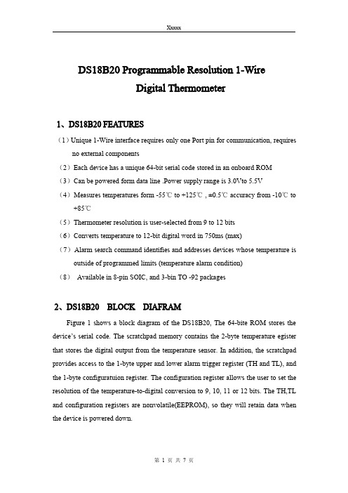
DS18B20Programmable Resolution1-WireDigital Thermometer1、DS18B20FEATURES(1)Unique1-Wire interface requires only one Port pin for communication,requires no external components(2)Each device has a unique64-bit serial code stored in an onboard ROM(3)Can be powered form data line.Power supply range is3.0Vto5.5V(4)Measures temperatures form-55℃to+125℃,±0.5℃accuracy from-10℃to +85℃(5)Thermometer resolution is user-selected from9to12bits(6)Converts temperature to12-bit digital word in750ms(max)(7)Alarm search command identifies and addresses devices whose temperature is outside of programmed limits(temperature alarm condition)(8)Available in8-pin SOIC,and3-bin TO-92packages2、DS18B20BLOCK DIAFRAMFigure1shows a block diagram of the DS18B20,The64-bite ROM stores the device’s serial code.The scratchpad memory contains the2-byte temperature egister that stores the digital output from the temperature sensor.In addition,the scratchpad provides access to the1-byte upper and lower alarm trigger register(TH and TL),and the1-byte configuratuion register.The configuration register allows the user to set the resolution of the temperature-to-digital conversion to9,10,11or12bits.The TH,TL and configuration registers are nonvolatile(EEPROM),so they will retain data when the device is powered down.Figure1block diagram of the DS18B203、DS18B20ROM COMMANDS(1)SEARCH ROM[0F0H]When a system is initially powered up,the master must identify the ROM codes of all slave devices on the bus,which allows the master to determine the number of slaves and their device types.The master learns the ROM codes through a process of elimination that requires the master to perform a Search ROM cycle as many times as necessary to identify all of the slave’s64-bit ROM devices.(2)READ ROM[55H]This command can only be used when there is one slave on the bus.It allows the bus master to read the slave`64-bit ROM code without using the Search ROM procedure.If this command is used when there is more than one slave present on the bus,a data collision will occur when all the slaves attempt to respond at the same time.(3)MATCH ROM[55H]The match ROM command followed by a64-bit ROM code sequence allows the bus master to address a specific DS18B20on a multidrop or single-drop bus.Only the DS18B20that exactly matches the64-bitROM code sequence will respond to thefunction command issued by the master;all other slaves on the bus will wait for a reset pulse.(4)SKIP ROM[0CCH]The master can use this command to address all devices on the bus simultaneously without sending out any ROM code information.Note that the Read Scratchpad command can follow the Skip ROM command only if there is a single slave device on the bus.In this case time is saved by allowing the master to read from the slave without sending the device’s64-bit ROM code.A Skip ROM command followed by a Read Scratchpad command will cause a data collision on the bus if there is more than one slave since multiple devices will attempt to transmit data simultaneously.(5)ALARM SEARCH[0ECH]The operation of this command is identical to the operation of the Search ROM command except that only slaves with a set alarm flag will respond.This command allows the master device to determine if any DS18B20s experienced an alarm condition during the most recent temperature conversion.Refer to the OPERATION-ALARM SIGNAING section for an explanation of alarm flag operation.(6)CONVERTT[44H]This command initiates a single temperature conversion.Following the conversion,the resulting thermal data is stored in the2-bute temperature register in the scratchpad memory and the DS18B20returns to its low-power idle state.If the device is being used in parasite power mode,within10us after this command is issued the master must enable a strong pullup on the1-Wire bus for the duration of the conversion as described in the POWERING THE DS18320section.If the DS18B20 is powered by an external supply,the master can issue read time slots after the Convert T command and the DS18B20will respond by transmitting a0while the temperature conversion is in Progress and a1when the conversion is done.In parasite power mode this notification technique cannot be used since the bus1is pulled high by the strong pullup during the conversion.(7)WRITE SCRACHPAD[4EH]This command allows the master to write3bytes of the data to the DS18B20’s scratchpad.The first data byte is writer into the TH register,the second byte is written into the TL register,and the third byte is written into the configuration register. Data must be transmitted least significant bit first.All three bytes must be written before the master issues a reset,or the data may be corrupted.(8)READ SCRACHPAD[0BEH]This command allows the master to read the contents of the scratchpad.The data transfer starts with the least significant bit of byte0and continues through the scratchpad until9byte(byte8-CRC)is read.The master may issue a reset to terminate reading at any time if only partof the scratchpad data is needed.(9)COPY SCRATCHPAD[48H]This command copies the contents of the scratchpad TH,TL and configuration registers to EEPROM.If the device is being used in parasite power mode,within 10us(max)after this command is issued the master must enable a strong pullup on the 1-Wire bus for at least10ms as described in the POWERING THE DS18B20section.(10)RECALL E2[B8H]This command recalls the alarm trigger values(TH and TL)and configuration data from EEPROM,respectively,in the scratchpad memory.The master device can issue read time slots following the Recall E2command and the DS18B20will indicate the status of the recall by transmitting0while the recall is in progress and1 when the recall is done.The recall operation happens automatically at power-up,so valid data is available in the scratchpad as soon as power is applied to the device.DS18B20单总线数字温度计1、DS18B20的特性(1)独特的单总线接口只占用一个I/O端口,而无需外围元件;(2)可以由总线提供电源,电压适用范围为3.0V~5.5V;(3)测量温度范围为-55℃~+125℃,在-10℃~+85℃范围内精度为±0.5℃;(4)每个DS18B20含有一个唯一的64位ROM编码;(5)用户可以通过编程实现9~12位的温度分辨率;(6)分辨率为12时最大转换时间为750ms;(7)报警搜索命令可识别哪片DS18B20温度超限;(8)采用3脚T0-92或8脚SOIC封装。
传感器技术论文中英文对照资料外文翻译文献
传感器技术论文中英文对照资料外文翻译文献Development of New Sensor TechnologiesSensors are devices that can convert physical。
chemical。
logical quantities。
etc。
into electrical signals。
The output signals can take different forms。
such as voltage。
current。
frequency。
pulse。
etc。
and can meet the requirements of n n。
processing。
recording。
display。
and control。
They are indispensable components in automatic n systems and automatic control systems。
If computers are compared to brains。
then sensors are like the five senses。
Sensors can correctly sense the measured quantity and convert it into a corresponding output。
playing a decisive role in the quality of the system。
The higher the degree of n。
the higher the requirements for sensors。
In today's n age。
the n industry includes three parts: sensing technology。
n technology。
and computer technology。
传感器技术10-数字传感器-中英对照

第10章 数字式传感器
结构组成
第10章 数字式传感器
基板(Foundation)上通过粘合剂(Adhesive)4粘有一层铜 箔(Copper foil)。铜箔厚度在0.lmm以下,通过蚀刻 (etching)得到所需的绕组(Winding)3的图形。在铜箔上 面是一层耐腐蚀的绝缘涂层1。根据需要还可在滑尺表 面再贴一层带绝缘层的铝箔(Aluminium foil)5,以防止 静电感应(Static Induction) 。
所谓鉴幅法就是根据感应电势的幅值来测量位移。若在感应同步 器滑尺的正弦和余弦绕组上分别加频率和相位相同、但幅值不等 的正弦激磁电压,即 uS U m sin sin t 和 uC U m cos sin t 。 则在定尺绕组上产生的感应电势分别为
es KU m sin cos t cos ec KU m cos cos t sin
第10章 数字式传感器
位移-相位转换的功能是通过感应同步器将位 移量转换为电的相位移。 模数转换的主要功能是将代表位移量θ(定尺 输出电压的相位)的变化再转换为数字量。 鉴相器是一个相位比较装置,其输人来自经放 大、滤波、整形后的输出信号e,以及相对相 位基准输出信号θ’o。 相对相位基准(脉冲移相器)实际上是一个数 模转换器、它是把加、减脉冲数转换为电的相 位变化。 模数转换的关键是鉴相器。
3.脉冲调宽法(Impulse Width Modulation) 前面介绍的两种方法都是在滑尺上加正弦激磁电 压,而脉冲调宽法则在滑尺的正弦和余弦绕组上分 别加周期性方波(Square Wave)电压,即
其波形如图10-8(a)所示。把us,uc分别用傅里叶级数 展开(Fourier series expansion) ,可得
外文翻译----数字温湿度传感器(SHT 1x SHT 7x)
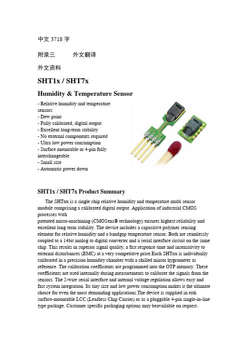
- Ultra low power consumption
- Surface mountable or 4-pin fully interchangeable
- Small size
- Automatic power down
SHT1x / SHT7x Product Summary
The SHTxx is a single chip relative humidity and temperature multi sensor module comprising a calibrated digital output. Application of industrial CMOS processes with
patented micro-machining (CMOSens® technology) ensures highest reliability and excellent long term stability. The device includes a capacitive polymer sensing element for relative humidity and a bandgap temperature sensor. Both are seamlessly coupled to a 14bit analog to digital converter and a serial interface circuit on the same chip. This results in superior signal quality, a fast response time and insensitivity to external disturbances (EMC) at a very competitive price.Each SHTxx is individually calibrated in a precision humidity chamber with a chilled mirror hygrometer as reference. The calibration coefficients are programmed into the OTP memory. These coefficients are used internally during measurements to calibrate the signals from the sensors. The 2-wire serial interface and internal voltage regulation allows easy and fast system integration. Its tiny size and low power consumption makes it the ultimate choice for even the most demanding applications.The device is supplied in eith surface-mountable LCC (Leadless Chip Carrier) or as a pluggable 4-pin single-in-line type package. Customer specific packaging options may beavailable on request.
数字温度传感器毕业论文中英文资料外文翻译文献[管理资料]
![数字温度传感器毕业论文中英文资料外文翻译文献[管理资料]](https://img.taocdn.com/s3/m/6bf8f73450e2524de4187ed1.png)
毕业论文中英文资料外文翻译文献外文资料DS1722 Digital ThermometerWith scientific and technological progress and development of the types of temperature sensors increasingly wide range of application of the increasingly widespread, and the beginning analog toward digital, single-bus, dual-bus and bus-3 direction. And the number of temperature sensors because they apply to all microprocessor interface consisting of automatic temperature control system simulation can be overcome sensor and microprocessor interface need signal conditioning circuit and A / D converters advant ages of the drawbacks, has been widely used in industrial control, electronic transducers, medical equipment and other temperature control system. Among them, which are more representative of a digital temperature sensor DS18B20, MAX6575, the DS1722, MAX6636 other. This paper introduces the DS1722 digital temperature sensor characteristics, the use of the method and its timing. Internal structure and other relevant content.FEATURES:Temperature measurements require no external components;Measures temperatures from -55°C to +120°C. Fahrenheit equivalent is -67°F to +248°F;Thermometer accuracy is ±°C;Thermometer resolution is configurable from 8 to 12 bits (°C to °C resolution);Data is read from/written to via a Motorola Serial Peripheral Interface (SPI) or standard 3-wire serial interface;Wide analog power supply range ( - );Separate digital supply allows for logic;Available in an 8-pin SOIC (150 mil), 8-pin USOP, and flip chip package;PIN ASSIGNMENTFIGURE 1 PIN ASSIGNMENTPIN DESCRIPTION:SERMODE - Serial Interface Mode.CE - Chip Enable.SCLK - Serial Clock.GND – Ground.VDDA - Analog Supply Voltage.SDO - Serial Data Out.SDI - Serial Data In.VDDD - Digital Supply Voltage.DESCRIPTION:The DS1722 Digital Thermometer and Thermostat with SPI/3-Wire Interface provides temperature readings which indicate the temperature of the device. No additional components are required; the device is truly a temperature-to-digital converter. Temperature readings are communicated from the DS1722 over a Motorola SPI interface or a standard 3-wire serial interface. The choice of interface standard is selectable by the user. For applications that require greater temperature resolution, the user can adjust the readout resolution from 8 to 12 bits. This is particularly useful in applications where thermal runaway conditions must be detected quickly.For application flexibility, the DS1722 features a wide analog supply rail of - . A separate digital supply allows a range of to . The DS1722 is available in an 8-pin SOIC (150-mil), 8-pin USOP, and flip chip package.Applications for the DS1722 include personal computers/servers/workstations, cellular telephones, office equipment, or any thermally-sensitive system.OVERVIEW:A block diagram of the DS1722 is shown in Figure 2. The DS1722 consists offour major components:1. Precision temperature sensor.2. Analog-to-digital converter.3. SPI/3-wire interface electronics.4. Data registers.The factory-calibrated temperature sensor requires no external components. The DS1722 is in a power conserving shutdown state upon power-up. After power-up, the user may alter the configuration register to place the device in a continuous temperature conversion mode or in a one-shot conversion mode. In the continuous conversion mode, the DS1722 continuously converts the temperature and stores the result in the temperature register. As conversions are performed in the background, reading the temperature register does not affect the conversion in progress. In the one-shot temperature conversion mode, the DS1722 will perform one temperature conversion, store the result in the temperature register, and then eturn to the shutdown state. This conversion mode is ideal for power sensitive applications. More information on the configuration register is contained in the “OPERATION-Programming”section. The temperature conversion results will have a default resolution of 9 bits. In applications where small incremental temperature changes are critical, the user can change the conversion resolution from 9 bits to 8, 10, 11, or 12. This is accomplished by programming the configuration register. Each additional bit of resolution approximately doubles the conversion time. The DS1722 can communicate using either a Motorola Serial Peripheral Interface (SPI) or standard 3-wire interface. The user can select either communication standard through the SERMODE pin, tying it to VDDD for SPI and to ground for 3-wire. The device contains both an analog supply voltage and a digital supply voltage (VDDA and VDDD, respectively). The analog supply powers the device for operation while the digital supply provides the top rails for the digital inputs and outputs. The DS1722 was designed to be Logic-Ready.DS1722 FUNCTIONAL BLOCK DIAGRAM Figure 2OPERATION-Measuring Temperature:The core of DS1722 functionality is its direct-to-digital temperature sensor. The DS1722 measures temperature through the use of an on-chip temperature measurement technique with an operating range from -55°to +120°C. The device powers up in a power-conserving shutdown mode. After power-up, the DS1722 may be placed in a continuous conversion mode or in a one-shot conversion mode. In the continuous conversion mode, the device continuously computes the temperature and stores the most recent result in the temperature register at addresses 01h (LSB) and 02h (MSB). In the one-shot conversion mode, the DS1722 performs one temperature conversion and then returns to the shutdown mode, storing temperature in the temperature register. Details on how to change the setting after power up are contained in the “OPERATION-Programming”section. The resolution of the temperature conversion is configurable (8, 9, 10, 11, or 12 bits), with 9-bit readings the default state. This equates to a temperature resolution of °C, °C, °C, °C, or °C. Following each conversion, thermal data is stored in the thermometer register in two’s complement format; the information can be retrieved over the SPI or 3-wire interface with the address set to the temperature register, 01h (LSB) and then 02h (MSB). Table 2 describesthe exact relationship of output data to measured temperature. The table assumes the DS1722 is configured for 12-bit resolution; if the evince is configured in a lower resolution mode, those bits will contain 0s. The data is transmitted serially over the digital interface, MSB first for SPI communication and LSB first for 3-wire communication. The MSB of the temperature register contains the “sign” (S) bit, denoting whether the temperature is positive or negative. For Fahrenheit usage, a lookup table or conversion routine must be used.AddressLocation S 2625242322212002h MSB (unit = ℃) LSB2-12-22-32-40 0 0 0 01hTEMPERATURE DIGITAL OUTPUT(BINARY) DIGITAL OUTPUT(HEX)+120℃0111 1000 0000 0000 7800h+ 0001 1001 0001 0000 1910h+ 0000 1010 0010 0000 0a20h+ 0000 0000 1000 0000 0080h0 0000 0000 0000 0000 0000h1111 1111 1000 0000 Ff80h1111 0101 1110 0000 F5e0h1110 0110 1111 0000 E6f0h-55 1100 1001 0000 0000 C900h OPERATION-Programming:The area of interest in programming the DS1722 is the Configuration register. All programming is done via the SPI or 3-wire communication interface by selecting the appropriate address of the desired register location. Table 3 illustrates the addresses for the two registers (configuration and temperature) of the DS1722.Register Address Structure Table 3CONFIGURATION REGISTER PROGRAMMING:The configuration register is accessed in the DS1722 with the 00h address for reads and the 80h address for writes. Data is read from or written to the configuration register MSB first for SPI communication and LSB first for 3-wire communication. The format of the register is illustrated in Figure 2. The effect each bit has on DS1722 functionality is described below along with the power-up state of the bit. The entire register is volatile, and thus it will power-up in the default state.CONFIGURATION/STATUS REGISTER Figure 21SHOT = One-shot temperature conversion bit. If the SD bit is "1", (continuous temperature conversions are not taking place), a "1" written to the 1SHOT bit will cause the DS1722 to perform one temperature conversion and store the results in the temperature register at addresses 01h (LSB) and 02h (MSB). The bit will clear itself to "0" upon completion of the temperature conversion. The user has read/write access to the 1SHOT bit, although writes to this bit will be ignored if the SD bit is a "0", (continuous conversion mode). The power-up default of the one-shot bit is "0".R0, R1, R2 = Thermometer resolution bits. Table 4 below defines the resolution of the digital thermometer, based on the settings of these 3 bits. There is a direct tradeoff between resolution and conversion time, as depicted in the AC Electrical Characteristics. The user has read/write access to the R2, R1 and R0 bits and the power-up default state is R2="0", R1="0", and R0="1" (9-bit conversions).THERMOMETER RESOLUTION CONFIGURATION Table 4SD = Shutdown bit. If SD is "0", the DS1722 will continuously perform temperature conversions and store the last completed result in the temperature register. If SD is changed to a "1", the conversion in progress will be completed and stored and then the device will revert to a low-power shutdown mode. The communication port remains active. The user has read/write access to the SD bit and the power-up default is "1" (shutdown mode).SERIAL INTERFACE:The DS1722 offers the flexibility to choose between two serial interface modes. The DS1722 can communicate with the SPI interface or with a standard 3-wire interface. The interface method used is determined by the SERMODE pin. When this pin is connected to VDDD SPI communication is selected. When this pin is connected to ground, standard 3-wire communication is selected.SERIAL PERIPHERAL INTERFACE (SPI):The serial peripheral interface (SPI) is a synchronous bus for address and data transfer. The SPI mode of serial communication is selected by tying the SERMODE pin to VDDD. Four pins are used for the SPI. The four pins are the SDO (Serial Data Out), SDI (Serial Data In), CE (Chip Enable), and SCLK (Serial Clock). The DS1722 is the slave device in an SPI application, with the microcontroller being the master. The SDI and SDO pins are the serial data input and output pins for the DS1722, respectively. The CE input is used to initiate and terminate a data transfer. The SCLK pin is used to synchronize data movement between the master (microcontroller) and the slave (DS1722) devices. The shift clock (SCLK), which is generated by the microcontroller, is active only when CE is high and during address and data transfer to any device on the SPI bus. The inactive clock polarity is programmable in somemicrocontrollers. The DS1722 offers an important feature in that the level of the inactive clock is determined by sampling SCLK when CE becomes active. Therefore, either SCLK polarity can be accommodated. There is one clock for each bit transferred. Address and data bits are transferred in groups of eight, MSB first.3-WIRE SERIAL DATA BUS:The 3-wire communication mode operates similar to the SPI mode. However, in 3-wire mode, there is one bi-directional I/O instead of separate data in and data out signals. The 3-wire consists of the I/O (SDI and SDO pins tied together), CE, and SCLK pins. In 3-wire mode, each byte is shifted in LSB first unlike SPI mode where each byte is shifted in MSB first. As is the case with the SPI mode, an address byte is written to the device followed by a single data byte or multiple data bytes.外文资料译文DS1722数字温度传感器随着科学技术的不断进步和发展,温度传感器的种类日益繁多,应用逐渐广泛,并且开始由模拟式向着数字式、单总线式、双总线式和三总线式发展。
单片机温度探测系统中英文对照外文翻译文献
中英文对照翻译附件1:外文资料翻译译文一种基于DS18B20的温度探测系统摘要所有的DS18B20传感器,用于多点温度测试,IO总线与MCU连接,温度数据的轮流收集。
如果系统有大量的传感器,MCU的时间用在处理温度数据明显延长,因此周期替代测试变得更长。
在本文中,一种新的方法,DS18B20的合理组合和一些在软件上采取的措施,替代试验进展速度明显。
关键词:DS18B20的集团,温度测试,轮流测试所花费的时间。
引言由于结构简单,安装方便,低损失和广泛的用途的温度测试,DS18B20温度测试传感器应用领域,需要多点温度测试,如化学工业,粮食,环境监督管理等。
因为通过一个DS18B20的多点温度测试系统总线,所有DS18B20是挂在一条总线上,然后每个温度测试点的值转换轮流读。
作为转换后读值必须阅读8次引脚的状态,移动时间,位置和存储数据,所以时间多花费在阅读每一个点的数据系统时间。
如果温度测试系统是大型系统由它造成的损失是相当多的,然后交替测试系统的运行速度明显降低,从而影响多点温度测试系统的效率。
在本文中,DS18B20的一些I / O总线上都挂着分组DS18B20的均匀,温度转换获取数据读取DS18B20的状态,系统损耗减少和替代测试速度增加显然,这将不会影响精度和转换的可靠性。
一套点对多点温度,在此实现人工环境实验室测试,这增加了测试效率。
作者对DS18B20的认识DS18B20是单总线数字温度传感器来自美国达拉斯公司。
DS18B20是由64数字光盘刻激光,温度敏感性组成部分,非易失性温度报警触发器(设备TH和TL)。
DS18B20的通信微处理器单总线端口和测试范围DS18B20是从-55摄氏度到+125摄氏度,增量值是0.5摄氏度。
温度可在720ms的数字改为每个DS18B20具有唯一的64数字序号。
图1揭示的具体内容:两个8的数字储量(0号和1号),用于存储在DS18B20的温度值。
0号存储存储器温度值,补充和一号存储器温度值的符号。
传感器温湿度测量中英文资料外文翻译文献
中英文资料外文翻译文献SHT11/71传感器的温湿度测量Assist.Prof.Grish Spasov,PhD,BSc Nikolay KakanakovDepartment of Computer Systems,Technical University-branch Plovdiv,25,”Tzanko Djustabanov”Str.,4000Plovdiv,Bulgaria,+35932659576, E-mail:gvs@tu-plovdiv.bg,kakanak@tu-plovdiv.bg 关键词:温湿度测量,智能传感器,分布式自动测控这篇论文阐述了智能传感器的优点,介绍了SHT11/71温湿度传感器(产自盛世瑞公司)。
该传感器是一种理想的对嵌入式系统提供环境测量参数的传感器。
常规的应用时将SHT11/71放于实际的工作环境当中。
应用于分布式的温湿度监测系统。
使用单片机与集成网络服务器来实现对传感器的信息交流与关系。
这个应用是可实现与测试的。
1.介绍温湿度的测量控制对于电器在工业、科学、医疗保健、农业和工艺控制过程都有着显著地意义。
温湿度这两种环境参数互相影响,因为这至关重要的一点,在一些应用中他们是必须并联测量的。
SHT11/71是利用现代技术把温度、湿度测量元件、放大器、A/D转换器、数字接口、校验CRC计算逻辑记忆模块和核心芯片集成到一个非常小的尺寸上[1][3]。
采用这种智能传感器可以缩短产品开发时间和成本。
整合入传感器模数转换和放大器的芯片使开发人员能够优化传感器精度和长期问的的元素。
并不是全结合形式的数字逻辑接口连通性管理的传感器。
这些优点可以减少整体上市时间,甚至价格[1][3]。
本文以SHT11/71(产自盛世瑞公司)智能传感器为例,介绍他的优势和测量程序给出一个实用实例来说明该工作的实现条件。
这个应用时可行可测试的。
2.智能传感器——SHT11/71SHT11/71是一个继承了温度和湿度组建,以及一个多元化校准数字器的芯片。
温度控制系统中英文对照外文翻译文献

温度控制系统中英文对照外文翻译文献温度控制系统中英文对照外文翻译文献(文档含英文原文和中文翻译)译文:温度控制系统的设计摘要:研究了基于AT89S 51单片机温度控制系统的原理和功能,温度测量单元由单总线数字温度传感器DS18B 20构成。
该系统可进行温度设定,时间显示和保存监测数据。
如果温度超过任意设置的上限和下限值,系统将报警并可以和自动控制的实现,从而达到温度监测智能一定范围内。
基于系统的原理,很容易使其他各种非线性控制系统,只要软件设计合理的改变。
该系统已被证明是准确的,可靠和满意通过现场实践。
关键词:单片机;温度;温度I. 导言温度是在人类生活中非常重要的参数。
在现代社会中,温度控制(TC)不仅用于工业生产,还广泛应用于其它领域。
随着生活质量的提高,我们可以发现在酒店,工厂和家庭,以及比赛设备。
而比赛的趋势将更好地服务于整个社会,因此它具有十分重要的意义测量和控制温度。
在AT89S51单片机和温度传感器DS18B20的基础上,系统环境温度智能控制。
温度可设定在一定范围内动任意。
该系统可以显示在液晶显示屏的时间,并保存监测数据,并自动地控制温度,当环境温度超过上限和下限的值。
这样做是为了保持温度不变。
该系统具有很高的抗干扰能力,控制精度高,灵活的设计,它也非常适合这个恶劣的环境。
它主要应用于人们的生活,改善工作和生活质量。
这也是通用的,因此它可以方便地扩大使用该系统。
因此,设计具有深刻的重要性。
一般的设计,硬件设计和软件系统的设计都包括在内。
II. 系统总体设计该系统硬件包括微控制器,温度检测电路,键盘控制电路,时钟电路,显示,报警,驱动电路和外部RAM。
基于AT89S51单片机,DS18B20的将温度信号传送到数字信号的检测。
和信号发送到微控制器进行处理。
最后,温度值显示在液晶12232F。
这些步骤是用来实现温度检测。
使用键盘接口芯片HD7279在设定温度值,使用微控制器保持一定的温度,并使用液晶显示的温度控制设定值。
- 1、下载文档前请自行甄别文档内容的完整性,平台不提供额外的编辑、内容补充、找答案等附加服务。
- 2、"仅部分预览"的文档,不可在线预览部分如存在完整性等问题,可反馈申请退款(可完整预览的文档不适用该条件!)。
- 3、如文档侵犯您的权益,请联系客服反馈,我们会尽快为您处理(人工客服工作时间:9:00-18:30)。
中英文资料外文翻译The introduction to The DS18B201. DESCRIPTIONThe DS18B20 digital thermometer provides 9-bit to 12-bit Celsius temperature measurements and has an alarm function with nonvolatile user programmable upper and lower trigger points. The DS18B20 communicates over a 1-Wire bus that by definition requires only one data line for communication with a central microprocessor. It has an operating temperature range of -55°C to +125°C and is accurate to ±0.5°C over the range of -10°C to +85°C. In addition, the DS18B20 can derive power directly from the data line (―parasite power‖), eliminating the need for an external power supply.Each DS18B20 has a unique 64-bit serial code, which allows multiple DS18B20s to function on the same 1-Wire bus. Thus, it is simple to use one microprocessor to control many DS18B20s distributed over a large area. Applications that can benefit from this feature include HV AC environmental controls, temperature monitoring systems inside buildings, equipment, or machinery, and process monitoring and control systems.2.FEATURES●Unique 1-Wire® Interface Requires Only One Port Pin for Communication●Each Device has a Unique 64-Bit Serial Code Stored in an On-Board ROM●Multi-drop Capability Simplifies Distributed Temperature-Sensing Applications ●Requires No External Components1●Can Be Powered from Data Line; Power Supply Range is 3.0V to 5.5V●Measures Temperatures from -55°C to +125°C (-67°F to +257°F)●±0.5°C Accuracy from -10°C to +85°C●Thermometer Resolution is User Selectable from 9 to 12 Bits●Converts Temperature to 12-Bit Digital Word in 750ms (Max)●User-Definable Nonvolatile (NV) Alarm Settings●Alarm Search Command Identifies and Addresses Devices Whose Temperature isOutside Programmed Limits●Software Compatible with the DS1822●Applications Include Thermostatic Controls, Industrial Systems, ConsumerProducts, Thermometers, or Any Thermally Sensitive System3.OVERVIEWFigure 1 shows a block diagram of the DS18B20, and pin descriptions are given in the Pin Description table. The 64-bit ROM stores the device’s unique serial code. The scratchpad memory contains the 2-byte temperature register that stores the digital output from the temperature sensor. In addition, the scratchpad provides access to the 1-byte upper and lower alarm trigger registers (TH and TL) and the 1-byte configuration register. The configuration register allows the user to set the resolution of the temperature to-digital conversion to 9, 10, 11, or 12 bits. The TH, TL, and configuration registers are nonvolatile (EEPROM), so they will retain data when the device is powered down.The DS18B20 uses Maxim’s exclusive 1-Wire bus protocol that implements bus communication using one control signal. The control line requires a weak pull up resistor since all devices are linked to the bus via a 3-state or open-drain port (the DQ pin in the case of the DS18B20). In this bus system, the microprocessor (the master device) identifies and addresses devices on the bus using each device’s unique 64-bit code. Because each device has a unique code, the number of devices that can be addressed on one DS18B20 bus is virtually unlimited. The 1-Wire bus protocol,2including detailed explanations of the commands and “time slots,‖ is covered in the 1-Wire Bus System section.Another feature of the DS18B20 is the ability to operate without an external power supply. Power is instead supplied through the 1-Wire pull up resistor via the DQ pin when the bus is high. The high bus signal also charges an internal capacitor (CPP), which then supplies power to the device when the bus is low. This method of deriving power from the 1-Wire bus is referred to as ―parasite power.‖ As an alternative, the DS18B20 may also be powered by an external supply on VDD.Figure 1.DS18B20 Block Diagram4.OPERATION—MEASURING TEMPERATURThe core functionality of the DS18B20 is its direct-to-digital temperature sensor. The resolution of the temperature sensor is user-configurable to 9, 10, 11, or 12 bits, corresponding to increments of 0.5°C, 0.25°C, 0.125°C, and 0.0625°C, respectively. The default resolution at power-up is 12-bit. The DS18B20 powers up in a low-power idle state. To initiate a temperature measurement and A-to-D conversion, the master must issue a Convert T [44h] command. Following the conversion, the resulting thermal data is stored in the 2-byte temperature register in the scratchpad memory and the DS18B20 returns to its idle state. If the DS18B20 is powered by an external supply, the master can issue ―read time slots‖ (see the 1-Wire Bus System section) after the Convert T command and the DS18B20 will respond by transmitting 0 while3the temperature conversion is in progress and 1 when the conversion is done. If the DS18B20 is powered with parasite power, this notification technique cannot be used since the bus must be pulled high by a strong pull up during the entire temperature conversion.The DS18B20 output temperature data is calibrated in degrees Celsius; for Fahrenheit applications, a lookup table or conversion routine must be used. The temperature data is stored as a 16-bit sign-extended two’s complement number in the temperature register (see Figure 2). The sign bits (S) indicate if the temperature is positive or negative: for positive numbers S = 0 and for negative numbers S = 1. If the DS18B20 is configured for 12-bit resolution, all bits in the temperature register will contain valid data. For 11-bit resolution, bit 0 is undefined. For 10-bit resolution, bits 1 and 0 are undefined, and for 9-bit resolution bits 2, 1, and 0 are undefined. Table 1 gives examples of digital output data and the corresponding temperature reading for 12-bit resolution conversions.5.64-BIT LASERED ROM CODE4Each DS18B20 contains a unique 64–bit code (see Figure 3) stored in ROM. The least significant 8 bits of the ROM code contain the DS18B20’s 1-Wire family code: 28h. The next 48 bits contain a unique serial number. The most significant 8 bits contain a cyclic redundancy check (CRC) byte that is calculated from the first 56 bits of the ROM code. The 64-bit ROM code and associated ROM function control logic allow the DS18B20 to operate as a 1-Wire device using the protocol detailed in the 1-Wire Bus System section.Figure 3.64-Bit Lasered ROM Code6.MEMORYThe DS18B20’s memory is organized as shown in Figure 4. The memory consists of an SRAM scratchpad with nonvolatile EEPROM storage for the high and low alarm trigger registers (TH and TL) and configuration register. Note that if the DS18B20 alarm function is not used, the TH and TL registers can serve as general-purpose memory.Byte 0 and byte 1 of the scratchpad contain the LSB and the MSB of the temperature register, respectively. These bytes are read-only. Bytes 2 and 3 provide access to TH and TL registers. Byte 4 contains the configuration register data. Bytes 5, 6, and 7 are reserved for internal use by the device and cannot be overwritten. Byte 8 of the scratchpad is read-only and contains the CRC code for bytes 0 through 7 of the scratchpad. The DS18B20 generates this CRC using the method described in the CRC Generation section.Data is written to bytes 2, 3, and 4 of the scratchpad using the Write Scratchpad [4Eh] command; the data must be transmitted to the DS18B20 starting with the least significant bit of byte 2. To verify data integrity, the scratchpad can be read (using the Read Scratchpad [BEh] command) after the data is written. When reading the scratchpad, data is transferred over the 1-Wire bus starting with the least significant56bit of byte 0. To transfer the TH, TL and configuration data from the scratchpad to EEPROM, the master must issue the Copy Scratchpad [48h] command.7.CONFIGURATION REGISTERByte 4 of the scratchpad memory contains the configuration register, which is organized as illustrated in Figure 5. The user can set the conversion resolution of the DS18B20 using the R0 and R1 bits in this register as shown in Table 2. The power-up default of these bits is R0 = 1 and R1 = 1 (12-bit resolution). Note that there is a direct tradeoff between resolution and conversion time. Bit 7 and bits 0 to 4 in the configuration register are reserved for internal use bythe device and cannot be overwritten.8.1-WIRE BUS SYSTEMThe 1-Wire bus system uses a single bus master to control one or more slave devices. The DS18B20 is always a slave. When there is only one slave on the bus, the system is referred to as a ―single-drop‖ system; the system is ―multi-drop‖ if there are multiple slaves on the bus. All data and commands are transmitted least significant bit first over the 1-Wire bus. The following discussion of the 1-Wire bus system is broken down into three topics: hardware configuration, transaction sequence, and1-Wire signaling (signal types and timing).9.TRANSACTION SEQUENCEThe transaction sequence for accessing the DS18B20 is as follows:Step 1. InitializationStep 2. ROM Command (followed by any required data exchange)Step 3. DS18B20 Function Command (followed by any required data exchange)It is very important to follow this sequence every time the DS18B20 is accessed, as the DS18B20 will not respond if any steps in the sequence are missing or out of order. Exceptions to this rule are the Search ROM [F0h] and Alarm Search [ECh] commands. After issuing either of these ROM commands, the master must return to Step 1 in the sequence.(1)INITIALIZATIONAll transactions on the 1-Wire bus begin with an initialization sequence. The initialization sequence consists of a reset pulse transmitted by the bus master followed7by presence pulse(s) transmitted by the slave(s). The presence pulse lets the bus master know that slave devices (such as the DS18B20) are on the bus and are ready to operate.(2)ROM COMMANDSAfter the bus master has detected a presence pulse, it can issue a ROM command. These commands operate on the unique 64-bit ROM codes of each slave device and allow the master to single out a specific device if many are present on the 1-Wire bus. These commands also allow the master to determine how many and what types of devices are present on the bus or if any device has experienced an alarm condition. There are five ROM commands, and each command is 8 bits long. The master device must issue an appropriate ROM command before issuing a DS18B20 function command.1.SEARCH ROM [F0h]When a system is initially powered up, the master must identify the ROM codes of all slave devices on the bus, which allows the master to determine the number of slaves and their device types. The master learns the ROM codes through a process of elimination that requires the master to perform a Search ROM cycle (i.e., Search ROM command followed by data exchange) as many times as necessary to identify all of the slave devices. If there is only one slave on the bus, the simpler Read ROM command can be used in place of the Search ROM process.2.READ ROM [33h]This command can only be used when there is one slave on the bus. It allows the bus master to read the slave’s 64-bit ROM code without using the Search ROM procedure. If this command is used when there is more than one slave present on the bus, a data collision will occur when all the slaves attempt to respond at the same time.3.MATCH ROM [55h]The match ROM command followed by a 64-bit ROM code sequence allows8the bus master to address a specific slave device on a multi-drop or single-drop bus. Only the slave that exactly matches the 64-bit ROM code sequence will respond to the function command issued by the master; all other slaves on the bus will wait for a reset pulse.4.SKIP ROM [CCh]The master can use this command to address all devices on the bus simultaneously without sending out any ROM code information. For example, the master can make all DS18B20s on the bus perform simultaneous temperature conversions by issuing a Skip ROM command followed by a Convert T [44h] command. Note that the Read Scratchpad [BEh] command can follow the Skip ROM command only if there is a single slave device on the bus. In this case, time is saved by allowing the master to read from the slave without sending the device’s 64-bit ROM code. A Skip ROM command followed by a Read Scratchpad command will cause a data collision on the bus if there is more than one slave since multiple devices will attempt to transmit data simultaneously.5.ALARM SEARCH [ECh]The operation of this command is identical to the operation of the Search ROM command except that only slaves with a set alarm flag will respond. This command allows the master device to determine if any DS18B20s experienced an alarm condition during the most recent temperature conversion. After every Alarm Search cycle (i.e., Alarm Search command followed by data exchange), the bus master must return to Step 1 (Initialization) in the transaction sequence.(3)DS18B20 FUNCTION COMMANDSAfter the bus master has used a ROM command to address the DS18B20 with which it wishes to communicate, the master can issue one of the DS18B20 function commands. These commands allow the master to write to and read from the DS18B20’s scratchpad memory, initiate temperature conversions and determine the power supply mode.91.CONVERT T [44h]This command initiates a single temperature conversion. Following the conversion, the resulting thermal data is stored in the 2-byte temperature register in the scratchpad memory and the DS18B20 returns to its low-power idle state. If the device is being used in parasite power mode, within 10µs (max) after this command is issued the master must enable a strong pull up on the 1-Wire bus. If the DS18B20 is powered by an external supply, the master can issue read time slots after the Convert T command and the DS18B20 will respond by transmitting a 0 while the temperature conversion is in progress and a 1 when the conversion is done. In parasite power mode this notification technique cannot be used since the bus is pulled high by the strong pull up during the conversion.2.READ SCRATCHPAD [BEh]This command allows the master to read the contents of the scratchpad. The data transfer starts with the least significant bit of byte 0 and continues through the scratchpad until the 9th byte (byte 8 – CRC) is read. The master may issue a reset to terminate reading at any time if only part of the scratchpad data is needed.3.WRITE SCRATCHPAD [4Eh]This command allows the master to write 3 bytes of data to the DS18B20’s scratchpad. The first data byte is written into the TH register (byte 2 of the scratchpad), the second byte is written into the TL register (byte 3), and the third byte is written into the configuration register (byte 4). Data must be transmitted least significant bit first. All three bytes MUST be written before the master issues a reset, or the data may be corrupted.4.COPY SCRATCHPAD [48h]This command copies the contents of the scratchpad TH, TL and configuration registers (bytes 2, 3 and 4) to EEPROM. If the device is being used in parasite power mode, within 10µs (max) after this command is issued the master must enable a10strong pull-up on the 1-Wire bus.5.RECALL E2 [B8h]This command recalls the alarm trigger values (TH and TL) and configuration data from EEPROM and places the data in bytes 2, 3, and 4, respectively, in the scratchpad memory. The master device can issue read time slots following the Recall E2command and the DS18B20 will indicate the status of the recall by transmitting 0 while the recall is in progress and 1 when the recall is done. The recall operation happens automatically at power-up, so valid data is available in the scratchpad as soon as power is applied to the device.6.READ POWER SUPPL Y [B4h]The master device issues this command followed by a read time slot to determine if any DS18B20s on the bus are using parasite power. During the read time slot, parasite powered DS18B20s will pull the bus low, and externally powered DS18B20s will let the bus remain high.10.WIRE SIGNALINGThe DS18B20 uses a strict 1-Wire communication protocol to ensure data integrity. Several signal types are defined by this protocol: reset pulse, presence pulse, write 0, write 1, read 0, and read 1. The bus master initiates all these signals, with the exception of the presence pulse.(1)INITIALIZATION PROCEDURE—RESET AND PRESENCE PULSES All communication with the DS18B20 begins with an initialization sequence that consists of a reset pulse from the master followed by a presence pulse from the DS18B20. This is illustrated in Figure 6. When the DS18B20 sends the presence pulse in response to the reset, it is indicating to the master that it is on the bus and ready to operate.During the initialization sequence the bus master transmits (TX) the reset pulse by pulling the 1-Wire bus low for a minimum of 480µs. The bus master then releases11the bus and goes into receive mode (RX). When the bus is released, the 5kΩ pull-up resistor pulls the 1-Wire bus high. When the DS18B20 detects this rising edge, it waits 15µs to 60µs and then transmits a presence pulse by pulling the 1-Wire bus low for 60µs to 240µs.TimingBus master pulling lowDS18B20 pulling lowResistor pullupFigure 6.Initialization Timing(2)READ/WRITE TIME SLOTSThe bus master writes data to the DS18B20 during write time slots and reads data from the DS18B20 during read time slots. One bit of data is transmitted over the 1-Wire bus per time slot.1.WRITE TIME SLOTSThere are two types of write time slots: ―Write 1‖ time slots and ―Write 0‖ time slots. The bus master uses a Write 1 time slot to write a logic 1 to the DS18B20 and a Write 0 time slot to write a logic 0 to the DS18B20. All write time slots must be a minimum of 60µs in duration with a minimum of a 1µs recovery time between individual write slots. Both types of write time slots are initiated by the master pulling the 1-Wire bus low (see Figure 7).To generate a Write 1 time slot, after pulling the 1-Wire bus low, the bus master must release the 1-Wirebus within 15µs. When the bus is released, the 5kΩ pull-up resistor will pull the bus high. To generate a Write 0 time slot, after pulling the 1-Wire1213bus low, the bus master must continue to hold the bus low for the duration of the time slot (at least 60µs).The DS18B20 samples the 1-Wire bus during a window that lasts from 15µs to 60µs after the master initiates the write time slot. If the bus is high during the sampling window, a 1 is written to the DS18B20. If the line is low, a 0 is written to the DS18B20.DS18B20Write Time SlotSTART OF SLOTVccBus master pulling low Resistor pullupFigure 7.DS18B20 Write Time Slot2.READ TIME SLOTSThe DS18B20 can only transmit data to the master when the master issues read time slots. Therefore, the master must generate read time slots immediately after issuing a Read Scratchpad [BEh] or Read Power Supply [B4h] command, so that the DS18B20 can provide the requested data. In addition, the master can generate read time slots after issuing Convert T [44h] or Recall E 2 [B8h] commands to find out the status of the operation.All read time slots must be a minimum of 60µs in duration with a minimum of a 1µs recovery time between slots. A read time slot is initiated by the master device pulling the 1-Wire bus low for a minimum of 1µs and then releasing the bus (see Figure 8). After the master initiates the read time slot, the DS18B20 will begin transmitting a 1 or 0 on bus. The DS18B20 transmits a 1 by leaving the bus high andtransmits a 0 by pulling the bus low. When transmitting a 0, the DS18B20 will release the bus by the end of the time slot, and the bus will be pulled back to its high idle state by the pull up resister. Output data from the DS18B20 is valid for 15µs after the falling edge that initiated the read time slot. Therefore, the master must release the bus and then sample the bus state within 15µs from the start of the slot.VccBus master pulling lowResistor pullupDS18B20 pulling lowFigure 8.DS18B20 Read Time Slot14DS18B20介绍1.说明DS18B20数字式温度传感器提供9位到12位的摄氏温度测量,并且有用户可编程的、非易失性温度上下限告警出发点。