MAX9724DEBC+TG45,MAX9724DETC+T,MAX9724CETC+T,MAX9724DETC+,MAX9724DEVKIT+, 规格书,Datasheet 资料
Google Pixel 6 Pro 128GB 说明书

Google Pixel 6 Pro 128GBGoogle Tensor Application Processor PoP(Tensor AP + Micron 12 GB LPDDR5 MT62F1536M64D8CH-031 WT:A)Kioxia 128 GB NAND Flash MemorySamsung SHANNON A5123 5G ModemSamsung SHANNON 5511 RF TransceiverMaxim MAX77759A PMICSTMicroelectronics NFC Controller ST54KMaxim MAX20339EWB Surge protection ICNXP PCA9468 Battery Charger ICSTMicroelectronics MCU ST33J2M0Google H1D3M Titan M security processorSamsung Exynos SM 5800 Supply Modulator (2 pcs)Cirrus Logic CS35L41B Audio Amplifier (2 pcs)Cirrus Logic CS40L25 Audio Amplifier HapticBroadcom BCM47765 GNSS Receiver ICFigure 1. Google Pixel 6 Pro Board ShotSkyworks SKY53737 FEMSkyworks SKY58260-11 FEMSamsung Exynos SM 5800 Supply ModulatorQorvo QM77080 FEMSkyworks SKY53738 FEM (3 pcs)Skyworks SKY77652-31 PAMSamsung Shannon 5311A PMICIDT P9412 Wireless Charing Receiver ICSamsung PMIC S2MPG10Samsung PMIC S2MPG11Unknown, Wi-Fi/BT Module (likely)Figure 2. Google Pixel 6 Pro Board ShotGoogle Tensor Application ProcessorGoogle’s semi-custom application processor is all about AI. Google built a custom deep learning accelerator (DLA) to challenge Qualcomm and Samsung in inferencing. The custom DLA features 16 (4x4) instantiations of systo lic arrays that outscore both Qualcomm and Samsung on ETH Zurich’s AI-Benchmark. While impressive, AI-Benchmark only tells half the story since it heavily relies on FP16 for inferencing. Most mobile AI network designers like to use INT8 for their layers because of the increased energy efficiency and comparable accuracy. For INT8 processing, the Pixel’s DLA lags both Qualcomm and Samsung in object detection, image segmentation, and image classification according to MLPerf 1.0.1 results.Figure 3. Google Deep Learning Accelerator (DLA)TechInsights' lab team has done a great job in getting the Google Tensor processor die photos quickly. The Tensor die has a die size (seal) of 10.38mm x 10.43mm = 108.26mm2 and is fabbed on Samsung's5nm process node technology. The following images show die marks and the die photo.Figure 4. Google Tensor Die MarkingsFigure 5. Google Tensor Package MarkingsThe die mark “S5P9845” conforms to the traditional Samsung Exynos processor naming rule, where the Exynos 990 Application Processor has the die marks of S5E9830, the Exynos 2100 5G SoC has die marks of S5E9840, and the Exynos 1080 5G SoC has S5E9815.We have heard of possible ties between the Google Tensor and Samsung Exynos processors, and our analysis of the Tensor die continues. It does appear that the foundry supplier for the Tensor die is Samsung. We will confirm the process node soon, which we ex pect is in Samsung’s 5LPE.Figure 6. Google Tensor Die PhotoSecurityGoogle designed the Titan M2, which is a custom RISC-V controller, to support Android Strongbox, securely generating keys, storing passwords, and protecting PINs. The company tested and certified its Titan chip through an external evaluation lab, achieving AVA_VAN.5 certification—one of the highest levels for smartphones.Mobile RF Components in the Google Pixel 6 ProOn the mobile RF front, the Pixel 6 brings about some key new developments:∙Google / Samsung ties in the Tensor: Now that we have spent some time examining the Google Tensor SoC, we have analyzed the device tree file system of the Linux kernel for Google Pixel 6, and it shows that some blocks of the Google GS101 Tensor processor are shared with Samsung’s Exynos.∙ A first for the US market: Samsung has developed a full 5G radio solution, which is included in the Pixel 6, making this the first major 5G phone in the US that does not include a Qualcommmodem.Looking forward, we note that Oppo is looking to develop their own SoC solutions for higher end phones - is Qualcomm’s dominance in this space diminishing?UWB ConnectivityConfirmed: the Google Pixel 6 Pro supports UWB connectivity, operating between 6489.6 MHz and 7987.2 MHz. Similar to the Galaxy S21 Ultra UWB design, the Google Pixel 6 Pro has multiple UWB patch antennas. However, in Google Pixel 6 Pro, only one antenna is used to transmit, whereas in the Galaxy S21 Ultra, two UWB antennas are used to send UWB signals.Although the Google Pixel 6 Pro design has similar components to the Samsung Galaxy S20 and Galaxy S21 Ultra, the Teardown team identified a new Qorvo UWB component instead of the same NXP SR100T that was found in the Samsung Galaxy S21 Ultra.WiFi 6EAnother point of similarity between the Google Pixel 6 Pro and the Samsung Galaxy S21 Ultra: the Pixel supports WiFi 6. This, however, is not just a protocol advancement - it requires new hardware designs. So far, we can confirm that the WiFi 6E modules from both phones include the Broadcom WiFi 6E SoC.Samsung Design WinsWith the exception of the Google Tensor Application Processor - which is now in our , the phone's key components are from Samsung, including: Samsung SHANNON A5123 5G Modem, Samsung SHANNON 5511 RF Transceiver, SHANNON 5800 Envelope Tracker IC, Samsung SHANNON 5311A PMIC, And more! The Samsung SHANNON A5123 5G Modem is not new to us. We originally found it in the Galaxy S20 Ultra in early 2020, where it paired with the Samsung Exynos 990 Application Processor as a standalone 5G Modem.As we have confirmed that there is a standalone Samsung 5G Modem in the Pixel 6 Pro, it stands to reason that the Google Tensor is an Application Processor without integrated Modem functionality, but we have not seen the die photos yet - we will confirm when we do.The Samsung SHANNON 5511 RF Transceiver is not new to us either. We originally found it in Samsung Exynos 1080 and 2100 5G SoC platform smartphones, such as Vivo X60 and Samsung Galaxy S21 series in early 2021.Additional Design WinsIn Memory, the Google Pixel 6 Pro we have torn down has a Micron 12 GB LPDDR5 which should have 8 pieces die of Micron’s 1y nm 12 Gb LPDDR5.KIOXIA has won the NAND Flash slot.There is a standalone GNSS Receiver IC from Broadcom. The BCM47765 is the company’s second generation Dual-Frequency (L1+L5) GNSS chip. TechInsights has analyzed the first generationBCM47755.The Pixel 6 Pro supports NFC and Wi-Fi/BT functions too. We have identified two likely modules and will confirm them through further analysis.STMicroelectronics keeps the NFC slot design win with the same die that we have seen in the Google Pixel 4 and Pixel 4 XL. We have confirmed that inside the wireless combo IC module is the Broadcom BCM4389 Wi-Fi 6E and Bluetooth 5 wireless combo SoC, which we first saw in the Samsung Galaxy S21 Ultra 5G phone.Google Pixel 6 Pro US Model GA03149-USWe have now done a quick tear down on a Google Pixel 6 Pro GA03149-US, a United States model of the phone that supports 5G mmWave and Sub-6.Comparison with the Canadian model we have been examining shows that the US model has a Samsung mmWave RF Transceiver Exynos RF 5710. So Samsung is the second silicon supplier of the 5G NR mmWave cellular chipsets, alongside Qualcomm. TechInsights will be creating a series of reverse engineering reports on the Exynos RF 5710 for our Mobile RF Analysis subscribers.We have also found a Murata mmWave Module SS1707051 found in the US phone. We are currently working to identify the die inside.Figure 7. Samsung mmWave RF Transceiver Exynos RF 5710Figure 8. Dual mmWave antenna module from Murata。
mimaki系列机器报错信息表

喷头出墨 !DO TEST DRAW 栈时间过
长
HEATER POWER OFF
加热器关 闭
PRE PRT AFT **C **C
加热器未 连接(左 BREAK 侧显示的 范例为前 加热器未 连接)
PRE PRT AFT **C **C
L.*>NC [JV5-01]
电热调节 器未连接 (左侧显 THERM 示的范例 为前加热 器的电热 调节器未 连接)
材料加热 器温度异 常
HEADWARM TEMP (---) HEADWARM BREAK (---) HEADWARM THERM (---)
喷头加热 器温度异 常
喷头加热 器未连接 喷头电热 调节器出 错
ERR212 WASTE INKTANK SENSOR
废墨瓶感 应器出错
ERR250 Y COORDINATES
SD-RAM控 制异常
收到的数 据不是版 本升级数 据
I/F板未 安装
I/F板操 作异常
主板与 I/F板连 接错误
电脑与 I/F板连 接超时
ROM0 清 除错误 ROM1 清 除错误 ROM0 写 入错误 ROM1 写 入错误 校验错误 无用信息 检查错误
ERR90 h'******* ERR92 h'******* ERR95 MODE SHIFT ERR98 I/F FORMAT ERR99 VERSION DATA ERR111 NCU ROM 00
**Washing liquid** **unfilling up**
清洁液未 注入
解决方法
相关描述
关闭电源 2-3分钟 后重新开 机如果问 题仍然出 现,联系 经销商。 关闭电源 2-3分钟 后重新开 机如果问 题仍然出 现,联系 经销商。 关闭电源 2-3分钟 后重新开 机如果问 题仍然出 现,联系 经销商。
新型键盘显示驱动芯片MAX6954及其应用
可用 以降低E 。 MI
主 要 弓 脚 功 能 l
P ~ 4 通 用 I 口 ,其 中 P ~ 3 0P: / 0 0 P 可 配 置 成 矩 阵 键 盘 的 输 入 ,但 应 带 有
一一 一洲 一一
内部 上 拉 ;P 则 可 配置 为 中断 请 求输 4
袁 泉 夏应 清 周 兆 丰 向 常 州 华中 师范大学物理科学与技术学院
引 言
允 段 、或 18 分 立 的 L D,且 电 源 电 压 模 式 、 限 制 扫 描 位 寄 存 器 ( 许 用 户 2个 E
. 选 择 1 1位 用 于 显 示 ) ~6 、段 闪 烁 控 制 在 工 业 控 制 和 仪 器 仪 表 中 ,通 常 可 低 至 27V。 此 外 ,该 器 件 还 包 括 5 I 条 / 展 ( 果 需 要 ,可 通 过 驱 动 器 实 现 同 步 ) O扩 如 、 需 要 有 显 示 和 键 盘 等 人 机 界 面 , 而 显
D0UT
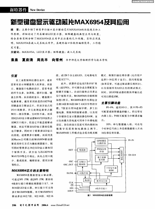
图 1 MAX 9 4的 功 能框 图 65
1 6 电 予 元 嚣 件 壶 硐 2 0 . W 'C ia C . t 0 0 66 W .hnE Dn W e
维普资讯
Ne De i e w v c
DO T:串行 数据 输 出端 。 由D N ◇ 数据 类型 寄存 器 U I 端 串 行输 入 的数 据 可 在 1.个 时 钟 周 5 5
结合 具 体 实例 分 析 了MAX6 5 在 应 用 中应 注 意 的几 个 问题 。 实际 应 用表 94 明 ,MAX6 5 在嵌入 式 系统 应 用 中,其硬 件接 I和 软件 编程 简单 ,工作稳 94 : 7
12位串行A_D转换器MAX1247原理与应用
12位串行A ΠD 转换器MAX 1247原理与应用王喜斌1 常淑英2(11华北航天工业学院 电子工程系,河北廊坊065000;21廊坊美联制动装置有限公司,河北廊坊065000)摘 要:M AX 1247是M AXI M 公司推出的4通道12位串行A ΠD 转换器,其内部具有SPI 串行接口,高速、低功耗。
本文详细介绍了M AX 1247的工作原理、工作时序及与单片机系统的接口电路及有关的读写程序。
关键词:单片机;模数转换器;M AX 1247;SPI中图分类号:TP335 文献标识码:A 文章编号:1009-2145(2004)01-0011-04收稿日期:2003-12-09作者简介:王喜斌(1968-),男,黑龙江华川人,工程师,长期从事计算机应用及自动控制方面的研究工作。
0 概 述MAX1247是美国MAXI M 公司推出的一种低功耗、4通道、12位串行模数转换芯片。
该芯片是一种逐次逼近式模数转换芯片,其内部自带与微处理器的串行接口SPI 。
同时,它还可以在连续转换模式下对外部4通道模拟输入信号进行顺序转换,且单一电源供电(217V ~5125V )。
与其他A ΠD 转换器相比,MAX1247具有较低的功耗和丰富的片上资源,且内部结构紧凑,集成度高,工作性能好,非常适用于便携式仪器仪表开发。
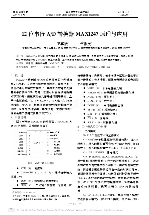
1 引脚说明图1所示为MAX1247的引脚图。
MAX1247具有16个引脚,各引脚定义如下:图1 MAX1247的引脚图● VDD(1):电源端;● CH0~CH3(2,3,4,5):模拟信号输入通道0~3;● C OM (6):模拟输入的参考地;● SH DN (7):关闭输入控制端,为低时,将使器件掉电;为高时,使参考缓冲区放大器处于内部补偿模式;将其浮动,则使参考缓冲区放大器处于外部补偿模式;● VREF (8):参考电压输入端;● REFAD J (9):参考缓冲放大器的输入端;● AG ND (10):模拟地;● DG ND (11):数字地;● DOUT (12):串行数据输出端;● SSTRB (13):转换结束;● DI N (14):数据输入端;● CS(15):片选端;● SC LK(16):时钟输入端;2 工作模式及工作时序211 工作模式MAX1247有以下4种工作模式:(1)UNI ΠBI (单极性转换Π双极性转换):在UNl模式下,输入的模拟量可在0V ~VREF 之间;在BI 模式下,输入的模拟量在2VREF/2~VREF/2之间;(2)FU LL POWER :掉电模式;(3)I NTERNA L C LOCK /EXTERNA L C LOCK (内时钟模式/外时钟模式):在外部时钟模式下,通过外部时钟控制数据的移入和移出,同时控制模数转换,因此要求模数转换必须在一定的时间内结束,否则转换结果将会降低,如果外部时钟的频率低于100kH z ,最好用内部时钟模式;在内部时钟模式下,MAX1247自动生成转换用时钟,无须单片机生成转换时钟,就可以读入A ΠD 转换的结果; (4)S NG LE/DIFFERE NTI A L (单极性输入模式Π双极性输入模式):在S NG LE 模式,由CH0、CH1、 第14卷第1期2004年3月 华北航天工业学院学报Journal of N orth China Institute of Astronautic Engineering V ol 114N o 11 Mar 12004CH 、CH3输入端信号分别和C OM 端口构成4路输入信号;在DIFFERE NTI A L 模式,CH0/CH1两输入端间将构成差动输入,CH2/CH3两输入端间将构成差分输入。
WAGO 750-559 4路 0-10VDC 分辨率12位数字输出模块说明书

https:///750-559This analog output module generates standard 0–10 V signals.The output signal is electrically isolated and transmitted with a resolution of 12 bits.The internal system supply powers the module.The module's output channels have a common ground potential.4-channel analog output; 0 ... 10 VDCData sheet | Item number: 750-559Color:light grayTechnical dataNumber of analog outputs 4T otal number of channels (module)4Signal type Voltage Signal type (voltage)0 … 10 VDC Actuator connection 4 x (2-wire)Resolution [bit]12 bitsData width4 x 16-bit data; 4 x 8-bit control/status (optional)Load impedance (voltage output)≥5 kΩConversion time (typ.)10 ms Output error, reference temperature25 °C Output error, deviation (max.) of the upper-range value 0.1 %T emperature error (max.) of the output range value 0.01 %/K Recovery time (typ.)100 msSupply voltage (system)5 VDC; via data contacts Current consumption (5 V system supply)125 mASupply voltage (field)24 VDC (-25 … +30 %); via power jumper contacts (power supply via blade contact;transmission via spring contact)Isolation500 V system/fieldNumber of incoming power jumper contacts2Number of outgoing power jumper contacts2Current carrying capacity (power jumper contacts)10 AConnection dataConnection technology: inputs/outputs8 x CAGE CLAMP®Connection type 1Inputs/outputsSolid conductor0.08 … 2.5 mm² / 28 … 14 AWGFine-stranded conductor0.08 … 2.5 mm² / 28 … 14 AWGStrip length8 … 9 mm / 0.31 … 0.35 inchPhysical dataWidth12 mm / 0.472 inchHeight100 mm / 3.937 inchDepth69.8 mm / 2.748 inchDepth from upper-edge of DIN-rail62.6 mm / 2.465 inchMechanical dataMounting type DIN-35 railMaterial dataColor light grayHousing material Polycarbonate; polyamide 6.6Fire load0.968 MJWeight51 gConformity marking CEEnvironmental requirementsAmbient temperature (operation)0 … +55 °CSurrounding air temperature (storage)-25 … +85 °CProtection type IP20Pollution degree (5) 2 per IEC 61131-2Operating altitude0 … 2000 m / 0 … 6562 ftMounting position horizontal (standing/lying); vertical Relative humidity (without condensation)95 %Vibration resistance4g per IEC 60068-2-6Shock resistance15g per IEC 60068-2-27EMC immunity to interference per EN 61000-6-2, marine applications EMC emission of interference per EN 61000-6-4, marine applications Exposure to pollutants per IEC 60068-2-42 and IEC 60068-2-43 S contaminant concentration at a relative humidity 75 %10 ppmPermissible H2contaminant concentration at a relative humidity 75 %25 ppmPermissible SO2Product Group 15 (Remote I/O)**********27-24-26-01*********27-24-26-01ETIM 7.0EC001596ETIM 6.0EC001596PU (SPU) 1 Stück Packaging typeBox Country of origin VKOrg Germany DEGTIN4045454490447Customs tariff number VKOrg Germany853********Approvals and certificatesEx-ApprovalsApprovalStandardCertificate nameATEXTUEV Nord Cert GmbH EN 60079-0CCCEx CQST/CNExCNCA-C23-012020312310000215 (Ex nA IIC T4 Gc)EACBrjansker ZertifizierungsstelleTP TC 012/2011EAC RU C-DE.AM02.B.00163/19 (2Ex nA IIC T4Gc X)IECExTUEV Nord Cert GmbH IEC 60079-0IECEx_TUN_14.0035_X (Ex ec IIC T4 Gc)INMETROTÜV Rheinland do Brasil Ltda.IEC 60079-0BR-Ex_TÜV 12.1297 XKTLKorea Testing Laboratory KOSHA Article 34,IEC60079-021-KA4BO-0551XULUnderwriters Laboratories Inc. (HAZARDOUS LOCATIONS)UL 121201E198726 Sec.1Country specific ApprovalsApprovalStandardCertificate nameKCNational Radio Research AgencyArticle 58-2, Clause 3MSIP-REM-W43-AOM750Ship Approvals ApprovalStandardCertificate nameABSAmerican Bureau of Shipping-22-2219060BSHBundesamt fuer Seeschifffahrt und Hydrographie-1104BVBureau Veritas S.A.-13453/E0 BV DNVDNV Germany GmbHDNV-CG-0339,Aug.2021TAA0000194Ship ApprovalsKRKorean Register of Shipping-KR HMB05880-AC001LRLloyds Register EMEA -02/20026 (E6)NKNippon Kaiji Kyokai -TA17255M PRSPolski Rejestr Statków -TE/2236/880590/19RINARINA Germany GmbH-ELE066419XGUL-ApprovalsApproval Standard Certificate name ULUL International Netherlands B.V. (ORDINARY LOCATIONS)UL 508E175199 Sec.1DownloadsEnvironmental Product ComplianceCompliance SearchEnvironmental ProductCompliance 750-559DocumentationManual4-channel, 0 - 10VDC V 1.2.0pdf3969.54 KBSystem Manual WAGO I/O System 750 / 753V 3.0.515.03.2022pdf8401.72 KBSystem Manual Series 750/753System Description750/753 Series I/O-System ‒ General Product Informationpdf953.35 KBOverview on WAGO-I/O-SYSTEM 750 approvalspdf770.48 KBUse in Hazardous EnvironmentsV 1.0.0pdf1007.06 KBAdditional InformationDisposal; Electrical and electronic equipment, Packaging V 1.0.0pdf259.56 KBBid Text750-55919.02.2019xml4.28 KB750-55905.03.2019docx17.24 KBausschreiben.de750-559CAD/CAE-DataCAD data2D/3D Models 750-559CAE dataEPLAN Data Portal 750-559WSCAD Universe 750-559ZUKEN Portal 750-559Device Driver WAGO USB Service Kabel Treiber / Serie 750und 8576.5.3.010.09.2014zip4721.96 KBDevice FilesSubject to changes. Please also observe the further product documentation! Current addresses can be found at: 。
GP ST3000系列全球代码列表主机模型号说明书
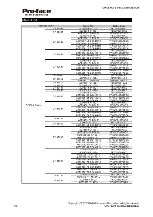
Main UnitModel No.Global Code AGP3200-A1-D24PFXGP3200AAD AGP3200-T1-D24PFXGP3200TAD AGP3200-T1-D24-M PFXGP3200TADC AGP3300-L1-D24PFXGP3300LAD AGP3300-L1-D24-M PFXGP3300LADC AGP3300-L1-D24-D81K PFXGP3300LADDK AGP3300-L1-D24-D81C PFXGP3300LADDC AGP3300-L1-D24-FN1M PFXGP3300LADFN AGP3300-L1-D24-CA1MPFXGP3300LADCA AGP3300-S1-D24PFXGP3300SAD AGP3300-S1-D24-D81K PFXGP3300SADDK AGP3300-S1-D24-D81C PFXGP3300SADDC AGP3300-S1-D24-CA1MPFXGP3300SADCA AGP3300-T1-D24PFXGP3300TAD AGP3300-T1-D24-M PFXGP3300TADC AGP3300-T1-D24-D81K PFXGP3300TADDK AGP3300-T1-D24-D81C PFXGP3300TADDC AGP3300-T1-D24-FN1M PFXGP3300TADFN AGP3300-T1-D24-CA1MPFXGP3300TADCA AGP3300-U1-D24PFXGP3300UAD AGP3301-L1-D24PFXGP3301LAD AGP3301-L1-D24-M PFXGP3301LADC AGP3301-S1-D24PFXGP3301SAD AGP3302-B1-D24PFXGP3302BAD AGP3310-T1-D24PFXGP3310TAD AGP3360-T1-D24PFXGP3360TAD AGP3400-S1-D24PFXGP3400SAD AGP3400-S1-D24-D81K PFXGP3400SADDK AGP3400-S1-D24-D81C PFXGP3400SADDC AGP3400-S1-D24-CA1MPFXGP3400SADCA AGP3400-T1-D24PFXGP3400TAD AGP3400-T1-D24-M PFXGP3400TADC AGP3400-T1-D24-D81K PFXGP3400TADDK AGP3400-T1-D24-D81C PFXGP3400TADDC AGP3400-T1-D24-FN1M PFXGP3400TADFN AGP3400-T1-D24-CA1MPFXGP3400TADCA AGP3450-T1-D24PFXGP3450TAD AGP3450-T1-D24-M PFXGP3450TADC AGP3500-L1-D24PFXGP3500LAD AGP3500-L1-D24-D81CPFXGP3500LADDC AGP3500-S1-AF PFXGP3500SAA AGP3500-S1-D24PFXGP3500SAD AGP3500-S1-D24-M PFXGP3500SADC AGP3500-S1-AF-D81K PFXGP3500SAADK AGP3500-S1-AF-D81C PFXGP3500SAADC AGP3500-S1-D24-D81K PFXGP3500SADDK AGP3500-S1-D24-D81C PFXGP3500SADDC AGP3500-S1-AF-CA1M PFXGP3500SAACA AGP3500-S1-D24-CA1MPFXGP3500SADCA AGP3500-T1-AF PFXGP3500TAA AGP3500-T1-D24PFXGP3500TAD AGP3500-T1-AF-D81K PFXGP3500TAADK AGP3500-T1-AF-D81C PFXGP3500TAADC AGP3500-T1-D24-D81K PFXGP3500TADDK AGP3500-T1-D24-D81C PFXGP3500TADDC AGP3500-T1-AF-FN1M PFXGP3500TAAFN AGP3500-T1-D24-FN1M PFXGP3500TADFN AGP3500-T1-AF-CA1M PFXGP3500TAACA AGP3500-T1-D24-CA1MPFXGP3500TADCA AGP3510-T1-AF PFXGP3510TAA AGP3510-T1-AF-CA1MPFXGP3510TAACA AGP3550-T1-AF PFXGP3550TAA AGP3550-T1-AF-MPFXGP3550TAACGP3000 SeriesGP-3310T GP-3360T GP-3500TGP-3400TGP-3510T GP-3550TGP-3301S GP-3200AGP-3300U GP-3302B GP-3301L Product NameGP-3450T GP-3500LGP-3500SGP-3200TGP-3300LGP-3300SGP-3300TGP-3400SModel No.Global Code AGP3560-T1-AF PFXGP3560TAA AGP3560-T1-AF-M PFXGP3560TAAC AGP3600-T1-AF PFXGP3600TAA AGP3600-T1-AF-M PFXGP3600TAAC AGP3600-T1-D24PFXGP3600TAD AGP3600-T1-D24-M PFXGP3600TADC AGP3600-T1-AF-D81K PFXGP3600TAADK AGP3600-T1-AF-D81C PFXGP3600TAADC AGP3600-T1-D24-D81K PFXGP3600TADDK AGP3600-T1-D24-D81C PFXGP3600TADDC AGP3600-T1-AF-FN1M PFXGP3600TAAFN AGP3600-T1-D24-FN1M PFXGP3600TADFN AGP3600-T1-AF-CA1M PFXGP3600TAACA AGP3600-T1-D24-CA1M PFXGP3600TADCA AGP3600-U1-D24-CA1MPFXGP3600UADCA AGP3650-T1-AF PFXGP3650TAA AGP3650-T1-AF-M PFXGP3650TAAC AGP3650-T1-D24-M PFXGP3650TADC AGP3650-U1-D24PFXGP3650UADC AGP3750-T1-AF PFXGP3750TAA AGP3750-T1-AF-M PFXGP3750TAAC AGP3750-T1-D24PFXGP3750TAD AGP3750-T1-D24-M PFXGP3750TADC AGP3300H-L1-D24PFXGP3300HLAD AGP3300H-S1-D24PFXGP3300HSAD AGP3310H-T1-D24PFXGP3310HTAD AST3201-A1-D24PFXST3201AAD AST3211-A1-D24PFXST3211AAD AST3301-B1-D24PFXST3301BAD AST3301-S1-D24PFXST3301SAD AST3301-T1-D24PFXST3301TAD AST3302-B1-D24PFXST3302BAD AST3401-T1-D24PFXST3401TAD AST3501-C1-AF PFXST3501CAA AST3501-C1-D24PFXST3501CAD AST3501-T1-AF PFXST3501TAA AST3501-T1-D24PFXST3501TADSoftware" ** " is changed with the version of software.Model No.Global CodeEX-EDV**PFXEXEDV**EXEDV**PFXEXEDV**EX-ED-LICENSE-V**PFXEXEDLSV**EX-SDV-V**PFXEXSDVV**EX-SED-LICENSEPFXEXSDLS EX-SRT-LICENSEPFXEXSRLS EX-MES-LICENSE-V**PFXEXMSLSV**EX-VIEWER-LICENSE PFXEXVW EX-VIEWER-LICENSE-10PFXEXVWLS10EX-VIEWER-LICENSE-30PFXEXVWLS30Camera Viewer EXEXCAVELS PFXEXCAVELS EX-RPA PFXEXRP EX-RPA-10PFXEXRPLS10EX-RPA-30PFXEXRPLS30EX-LADM-MIT-Q02PFXEXLMQ2LS EX-LADM-MIT-A01PFXEXLMA1LS EX-LADM-OMR-CJ01PFXEXLMCJ1LSEX-MOVCON-LICENSEPFXEXMCLS EX-WINGP-IPCPFXEXWGIP EX-WINGP-PCATPFXEXWGPC ST-3401T ST-3501C ST-3501TST-3301B GP-3650T GP-3650U GP-3750T GP-3300HL ST-3211A ST-3201A GP-3560T Product NameGP-3600TGP-3600TGP-3600U ST-3301S ST-3301T ST-3302B GP-3300HS GP-3310HT Product Name GP-Pro EX Editor License GP-Pro EX V*.*Pro-Server EX DeveloperPro-Server EX Developer License Pro-Server EX Runtime LicenseMES Action LicenseVideo Converter LicenseLadder Monitor License WinGP for IPC WinGP for PC/ATST3000 SeriesGP3000 SeriesSingle license10 licenses30 licensesRPA Client License GP-Viewer EX 10 licenses30 licenses Single license Single licenseExpansion UnitModel No.Global Code CA5-PFSALL/EX-01PFXZC5EUPFS CA6-DNSALL/EX-01PFXZC6EUDNS1CA9-CANALL/EX-01PFXZC9EUCA1CA7-CCLALL/EX-01PFXZC7EUCL1GP3000-VM01PFXZGPEUVM31GP2000-VM41PFXZGPEUVM21GP3000-DVI01PFXZGPEUDV01GP3000-RGB201PFXZGPEURG215m FP-DV01-50PFXZC0CBDV5110mFP-DV01-100PFXZC0CBDV1015m CA7-CBLCVRGB-01PFXZC7CBCVRG515mCA9-USBAMB/5M-01PFXZC9CBUSMB514.5m FP-CV02-45PFXZC0CBRG451CA9-USBATRGB/MB-01PFXZC9CLUSATRG1Model No.Global Code FN-XY32SKS41PFXZFNXY32K FN-X32TS41PFXZFNX32TS FN-XY16SK41PFXZFNXY16K FN-XY16SC41PFXZFNXY16C FN-Y08RL41- *FN-AD02AH41PFXZFNAD2FN-DA02AH41PFXZFNDA2FN-AD04AH11PFXZFNAD4FN-DA04AH11PFXZFNDA410m FN-CABLE2010-31-MS - *50mFN-CABLE2050-31-MS PFXZCBFN50200mFN-CABLE2200-31-MSPFXZCBFN200*There's no global code added for the products whose last order had been completed by December 31, 2011.Model No.Global Code HTB1C0DM9LP PFXHTB1C0DM9LP EXM-DDI8DT PFXZLTEUDDI8DT EXM-DDI16DT PFXZLTEUDDI16DT EXM-DRA8RT PFXZLTEUDRA8RT EXM-DRA16RT PFXZLTEUDRA16RT EXM-DDO8UT PFXZLTEUDDO8UT EXM-DDO16UK PFXZLTEUDDO16UK EXM-DDO8TT PFXZLTEUDDO8TT EXM-DDO16TK PFXZLTEUDDO16TK EXM-DMM8DRT PFXZLTEUDMM8DRT EXM-DMM24DRF PFXZLTEUDMM24DRF EXM-AMI2HT PFXZLTEUAMI2HT EXM-ALM3LT PFXZLTEUALM3LT EXM-AMM3HT PFXZLTEUAMM3HT EXM-AMO1HT PFXZLTEUAMO1HT EXM-AMI4LT PFXZLTEUAMI4LT EXM-AVO2HT PFXZLTEUAVO2HT EXM-AMM6HT PFXZLTEUAMM6HT EXM-ARI8LTPFXZLTEUARI8LTDVI-I/RGB Conversion Cable USB Cable for RGB Input Unit Analog RGB Cable USB Cable anti-disconnect holder (RGB Input Unit Side-miniB)4-ch Analog Input/ 2-ch Analog OutputModule8-ch Thermocouple Pt100/ Pt1000 InputModuleProduct Name2-channel Analog/Digital Conversion Unit 2-channel Digital/Analog Conversion Unit 4-channel Analog/Digital Conversion Unit VM Unit DVI Input Unit RGB Input UnitDVI-D CableCC-Link UnitProduct Name CANopen Slave UnitPROFIBUS Slave Unit DeviceNet Slave Unit 2-ch Analog Output Module32-point Input Sink/Source and 32-pointTransistor Output Sink Type 32-point Input Sink / Source Type 16-point Input Sink/Source and 16-pointTransistor Output Sink Type16-point Input Sink/Source and 16-pointTransistor Output Source type4-channel Digital/Analog Conversion UnitFLEX NETWORKCommunication Cable8-point Relay 0utput and 1 Common Type 4-ch Analog Input/ Thermocouple InputModuleCANopen Slave HTB Unit 8-Point Input Module 8-Point Relay Output Module 8-Point Sink Output Module 8-Point Source Output Module 2-ch Analog Input / 1-ch Analog OutputModule16-Point Sink Output Module 16-Point Source Output Module16-Point Input/ 8-point Relay Output Module 4-Point Input / 4-Point Relay Output Module 2-ch Thermocouple Pt100 Input / 1-ch AnalogOutput Module1-ch Analog Output Module16-Point Input Module 16-Point Relay Output Module 2-ch Analog Input ModuleProduct NameOptionsModel No.Global Code 5m CA3-CBL232/5M-01PFXZC3CBR2515m CA3-CBL422-01PFXZC3CBR4525m CA3-CBL422/5M-01PFXZC3CBR4515m CA3-CBLA-01PFXZC3CBA515m CA3-CBLQ-01PFXZC3CBQ515m CA3-CBLLNKMQ-01PFXZC3CBQL515m CA3-CBLFX/5M-01PFXZC3CBFX511m CA3-CBLFX/1M-01PFXZC3CBFX115m CA3-CBLSYS-01PFXZC3CBSYS515m CA6-CBLTTY/5M-01PFXZC6CBTTY51ST03-A2B-MPI21-PFE PFXZGPCBMPPE1GP3000-MPI21-PFE PFXZGPCBMPPE4CA3-MPIPG1-PFE PFXZGPCBMPPE5CA3-MPIPGN-PFE PFXZGPCBMPPE65mCA3-CBLMLT-01PFXZC3CBML120cmCA3-CBLCBT232-01PFXZC3CBCVR2120cmCA3-CBLCBT422-01PFXZC3CBCVR41GP070-MD11PFXZGPADMD15m CA3-MDCB11PFXZC3CBMD1CA3-ADPCOM-01PFXZC3ADCM1CA4-ADPONL-01PFXZC4ADCM1CA3-ADPTRM-01PFXZC3ADR41CA3-ADPSEI-01PFXZC3ADSE1CA3-ISO232-01PFXZC3ADISR21CA3-ISO485-01PFXZC3ADISR812mCA3-USBCB-01PFXZC3CBUSA15m FP-US00PFXZC0CBUS11mCA5-USBEXT-01PFXZC5CBUBEX150cmCA6-USB232-01PFXZC6CBCVUSR21RS-232C 9-pin/25-pin ConversionCableRS-485 Isolation Unit Siemens TTY Converter CableMitsubishi PLC Q Series Link Cable RS-422 Cable (Socket Type)Mitsubishi PLC A-SeriesConnection Cable Mitsubishi PLC Q-SeriesConnection Cable 3.5mProduct NameRS-232C CableRS-232C Isolation Unit RS-422C 9-pin/25-pin ConversionCable2-port Adapter II Cable 2-port Adapter IICOM Port Conversion AdapterOnline AdapterUSB Transfer Cable Multi-Link Cable Omron PLC SYSMAC Link Cable Terminal Block Conversion Adapter Siemens COM Port Conversion AdapterRS-422 Cable (Plug Type)MPI CableUSB cable USB Front Cable USB-Serial (RS-232C) ConversionCableMitsubishi PLC FX-SeriesConnection CableModel No.Global Code AGP3000H-ADPCOM-01PFXZGPADCM3H13m GP3000H-CBLS-3M PFXZGPCBS315m GP3000H-CBLS-5M PFXZGPCBS5110m GP3000H-CBLS-10M PFXZGPCBS10110m GP3000H-CBLH-10M PFXZGPCBH1013m GP3000H-CBLSD-3M PFXZGPCBSD315m GP3000H-CBLSD-5M PFXZGPCBSD5110m GP3000H-CBLSD-10M PFXZGPCBSD10110mGP3000H-CBLHD-10M PFXZGPCBHD101GP2000H-AP232PFXZGPADR22H GP2000H-AP422PFXZGPADR42H 3m GP3000H-CBLSD232-3M PFXZGPCBSDR231110m GP3000H-CBLSD232-10M PFXZGPCBSDR21013m GP3000H-CBLSD422-3M PFXZGPCBSDR43110mGP3000H-CBLSD422-10M PFXZGPCBSDR4101GP3000H-WMA-01PFXZGPADWMA1GP2000H-STRAP11PFXZGPST2H2128MB CA3-CFCALL/128MB-01PFXZC3CF1281256MB CA3-CFCALL/256MB-01PFXZC3CF2561512MB CA3-CFCALL/512MB-01PFXZC3CF51211GB CA6-CFCALL/1GB-01PFXZC6CF112GB CA8-CFCALL/2GB-01PFXZC8CF21GP077-CFAD10PFXZC0ADCF1GP3000-EXDM01PFXZGPIUEXDM CA6-DFS4-01PFXZC6DS41GP3000H-DFS6-01PFXZGPDS3H61CA3-DFS6-01PFXZC3DS61PS400-DF00PFXZGPDS71CA5-DFS10-01PFXZC5DS101CA3-DFS12-01PFXZC3DS121CA3-DFS15-01PFXZC3DS151CA4-DCMDL-01PFXZC4CNDCM1CA8-ODP10-01PFXZC8OP101GP077-SDAD10PFXZC0ADSJ1CA7-TPPEN/ALL-01PFXZC7TPP1CA4-ATM5-01PFXZC4AT61CA4-ATM10-01PFXZC4AT101for 3.8 inch for GP3000H CF CardNeck Strap GP3000H Soft-type Cable (RS-422) for GP2000H Conversion Adapter (with connector)GP3000H Soft-type Cable (RS-232C) for GP2000H ConversionAdapter (with connector)CF Card AdapterFunction Expansion MemoryPin Jack AdapterTouch Penfor 10.4 inch (TFT)GP2000H Series RS-422 Conversion Adapter Wall Hanging AdapterGP2000H Series RS-232C Conversion Adapter for 15 inch Screen ProtectionSheetfor 5.7 inch for 10.4 inch (TFT)for 5.7 inch for 7.5 inch GP3000H Soft-type Direct-connectCable (with connector)GP3000H Hard-type 10 m Direct-connect Cable (with connector)GP3000H Conversion AdapterGP3000H Soft-type Direct-connectCable GP3000H Hard-type 10m Direct-connect Cable for 12.1 inch/10.4inch(STN)for 5.7 inchfor 10.4 inch (TFT)Panel Cutout AdapterEnvironmentally-resistant CoverProduct NamePlease purchase when the products is damaged or lost.Model No.Global CodeCA6-FNCNALL-01PFXZC6CNFN1GLC-DIOCN03PFXZFNCNXY641CA7-HTBCNSET-01PFXZC7CNHTB1CA6-EXMCNHE20P-01PFXZC6CNEXHE201CA6-EXMCNRS11P-01PFXZC6CNEXRS111CA6-EXMCNRS10P-01PFXZC6CNEXRS101CA5-USBATM-01PFXZC5CLUSBM CA8-USBATALL-01PFXZC8CLUSB1CA5-USBATL-01PFXZC5CLUSBL GP3000H-DUPS-01PFXZGPDUPS1GP3000H-HS-01PFXZGPHS1GP3000H-EMGD-01PFXZGPEMGD1GP3000H-WPGADP-01PFXZGPWGHAD1CA5-BLU10T-01PFXZC5BL101CA6-BLU10T-02PFXZC6BL101PS501S-BU00PFXZGPBL102CA3-BLU12-01PFXZC3BL121CA3-BLU15-01PFXZC3BL151ST400-WP01PFXZSTWG41CA3-WPG6-01PFXZC3WG61CA5-WPG8-01PFXZC5WG81CA5-WPG10-01PFXZC5WG101CA3-WPG12-01PFXZC3WG121CA3-WPG15-01PFXZC3WG151CA3-ATFALL-01PFXZC3AT1CA3-BUSCVR-01PFXZC3CVBUS1CA5-DCCNM-01PFXZC5CNDCM1CA5-DCCNL-01PFXZC5CNDCL1CA5-AUXCNALL-01PFXZC5CNAX1CA6-DIOCNALL-01PFXZC6CNXY81Product NameAUX Connector DIO ConnectorUSB Cable Clamp (1 port) USB Cable Clamp (1 port) USB Cable Clamp (2 ports) Installation Gasket Function Switch SheetHand StrapEmergency Stop Switch Guard64-point DIO Connector Terminal Connector (10 pin) for EX moduleDIO Connector for HTBMIL Connector (20 pin) for EX module Terminal Connector (11 pin) for EX module FLEX NETWORK Connector for 7.5 inch for 10.4 inch (TFT)for 12.1 inch /10.4 inch(STN)for 10.4 inch(TFT)for 12.1 inch for 15 inch for 3.8 inch for 10.4 inch or largerDC Power SupplyConnectorfor 15 inchInstallation GasketInstallation Fastener Bus Connector CoverReplacement Backlightfor 7.5 inch/5.7 inch/3.8 inchfor 5.7 inch。
MAX793T中文资料
Voltage Can Exceed VCC o On-Board Gating of Chip-Enable Signals—7ns
Max Propagation Delay
元器件交易网
19-0366; Rev 1; 1/96
MAX793/MAX794/MAX795
3.0V/3.3V Adjustable Microprocessor Supervisory Circuits
_______________General Description
MAX793
WDO
CE IN
MR
WDI
PFO
LOWLINE
ADDRESS DECODER
VCC
VCC A0-A15
I/O NMI
µP
PFI
RESET
BATT OK
GND
RESET
________________________________________________________________ Maxim Integrated Products 1
Output Current VOUT................................................................................200mA All Other Outputs ..............................................................20mA
Pin Configurations appear at end of data sheet.
PRIMERGY RX2540 M4 2U 机械服务器系统配置器和订单信息指南说明书
5GFX _FPGA FPGA-cards, Graphics-, Grid-cards, GPU and Xeon Co processorsand other graphics optionsHD_cage Base CPU RAM List of content, Instructions for usage of this configurator,abbreviationsdescribes base unit of RX2540 M4Description System Description for easier understandingdescribes rack mount kits and servicesLTO drives & RDX drivePRIMERGY RX2540 M42U Rack Server16414LAN ComponentsFibre Channel ControllerInfiniband Controlleroptical disk drives (DVD, DVD-rw, Blu ray)Storage drives - PCIe SSD - SAS/SATA SSD & HDDOrder code and Infos of Intel® Xeon® Processor Scalable Family CPUs DDR4 System memory (RAM) and memory modesDrive cage and PCIe riser optionsSAS / RAID Controller and componentsChapter 32Folder Cover 79LAN_FC_IB ContentBackup RAID ODD HD_SSD 813101112System Management, ATD, RS232 port, TPM modulePower supply units, power cables, country specific opt.15PSU USB_devices others 16Keyboards, Mice, USB devices<-- order code E-part (bold) -- <-- order code L-part (bold)<-- "name" of this part <--description of this part, in same cases as well description of content <--requires a free PCIe slot --> means total amount of PCIe slots reduced <--indicates how often this part can be configured in the related ServerFor further information see:Link to datasheet:http:// xxxFujitsu is providing the content of this document with very high accuracy. In case you identify a mistake, we would kindly encourage you to inform us. We kindly ask for understanding, that errors still may occur and that Fujitsu may change this document without noticeText fields with grey color offer extra information for related topics (e.g prerequesites, technical background, configuration rules, limitations, …ge hout noticePRIMERGY RX2540 M4 schematics of the System boardPRIMERGY RX2540 M4 rear view with 2x PSU, 4x rear SFF or PCIe riser option and dynamic LoMrecommended components for RX2540 M4#PRIMERGY RX2540 M4 front view with drives and operation panelModular PSU 450W platinum hot plug 1x 1x 1x 2xPLAN EM 4x1Gb T interface card 1x Independant Mode installation Region kit APAC/EMEA/India iRMC advanced packcnfgRX2540M4.xlsx base Page 9 of 53Rack version for 19'' racks with 2 height unitsNo PSU included in base unitBasic unit is without CPU and MemoryFor an orderable basic unit first CPU andone memory = first memory has to be selectedBasic units LFF with4x 3.5" HDD bays S26361-K1567-V104Option upgrade 4x LFF S26361-F2495-E108No CPU TDP limitation with ATD40 option,ATD45 max 150W! No 4x rear SFF option!12x 3.5" HDD bays S26361-K1567-V112Including SAS expander for 8 channel controllerNo limitation for CPU TDP, no ATD40/45 option************************************.Mix of PRAID EP4xxi or PRAID CP4xxi with EP5xxi is not allowedBasic units SFF with8x 2.5" HDD bays S26361-K1567-V408Option upgrade 8x SFF S26361-F2495-E416No CPU TDP limitation with ATD40 option,ATD45 max 150W! No 4x rear SFF option!16x 2.5" HDD bays S26361-K1567-V216Without SAS expander for configuration with- 2x HBA or RAID controllers (mirrored) or- 16 channel PRAID EP540iNo CPU TDP limitation with ATD40 option,ATD45 max 150W! No 4x rear SFF option!Mix of PRAID EP4xxi or PRAID CP4xxi with EP5xxi is not allowed24x 2.5" HDD bays S26361-K1567-V424No limitation for CPU TDP, no ATD40/45 option************************************.Mix of PRAID EP4xxi or PRAID CP4xxi with EP5xxi is not allowedcnfgRX2540M4.xlsx base Page 10 of 53Beneath this five standard basic units there are use case specific basic units available.These may be pre-configured with special components according workload and optimized for a specific use case.There might be different configuration restrictions compared to the seven standard basic units, too…3x 8x 2.5" HDD bays S26361-K1567-V238VSAN ready node without SAS expander with- 3x HBA or RAID 8 channel controllers (Triple)or 2x 16-channel-ctrl PRAID EP540i/580iplus 4x rear SAS/SATA option @ same ctrl. (140W)No limitation for CPU TDP, no ATD40/45 option************************************.Basic units SFF optimized for Internal Storage28x 2.5" big single storage S26361-K1567-V428Configuration includes SAS expander, needs 1x PRAID EP5x0iand has option for 4x 2.5" rear option (SAS or PCIe)No limitation for CPU TDP, no ATD40/45 option4x rear SFF option with max. 140W @ same ctrl.Mixed SAS/PCIe planned for Q4/2018 ->Basic units LFF optimized for Internal Storage12x 3.5" +4x 2.5" big single storage S26361-K1567-V116Configuration includes SAS expander, needs 1x PRAID EP5x0iand has option for 4x 2.5" rear option (SAS or PCIe)No limitation for CPU TDP, no ATD40/45 option************************************.Mixed SAS/PCIe planned for Q4/2018 ->Basic unit SFF optimized for Flash applications (PCIe SSD)8x 2.5" + 4x PCIe SSD basic hybrid flash S26361-K1567-V884Configuration requires 1x Retimer or PRAID EP54/80i for 4x PCIe SSD eachNo mix of Retimers and PRAID EP54/80i allowed!4x to 8x PCIe SSD upgrade option available S26361-F2495-E884 / L884No CPU TDP limitation with ATD40 option,************************************.PRAID EP540/80i: max. 3x NVMe, + 1 additional PRAID EP5xxi for SAS/SATAHW-RAID NVMe requires VS35 and S26361-F3776-E900Basic units Liquid Cooled for Performance Storage applications24x 2.5" LC big performance storage S26361-K1567-V724 Configuration includes SAS exp., LC kit for CPUs and memoryand has option for 4x 2.5" rear option (SAS or PCIe) withno limitation for CPU 205W and ambient temperature max 45°C!On special release only!Mix of PRAID EP4xxi or PRAID CP4xxi with EP5xxi is not allowedBasic units for best graphics applications8x 2.5" best graphics S26361-K1567-V308 Configuration includes kit for first GPU/graphics card!8x 2.5" upgrade option limits to 1x GPU only!S26361-F2495-E416 New limitation: CPU max 165W with ambient temperature max 35°C!4x 3.5" best graphics S26361-K1567-V304 Configuration includes kit for first GPU/graphics card!4x 3.5" upgrade option has no limitation S26361-F2495-E108 New limitation: CPU max 165W with ambient temperature max 35°C!PRIMECENTER Rackrequiredrequired if 2nd CPUBank Iis configured Bank IIoptional, same type in Bank per CPU optional, any typerequiredrequired if 2nd CPU Bank I is configured Bank II optional, same type in Bank per CPU optional, any typeC h a n n e l AC h a n n e l BC h a n n e l CC h a n n e l DC h a n n e l EC h a n n e l MC h a n n e l FC h a n n e l GC h a n n e l HC h a n n e l JC h a n n e l KC h a n n e l LC h a n n e l KC h a n n e l LC h a n n e l MC h a n n e l AC h a n n e l BC h a n n e l CC h a n n e l DC h a n n e l EC h a n n e l FC h a n n e l GC h a n n e l HC h a n n e l Jrequiredrequired if 2nd CPU Bank I Spare Spare Spare Spare Spare SpareSpare SpareSpare SpareSpare Spare is configured(black sockets)Bank II Data DataDataDataDataDataDataDataDataDataDataDataoptional, same type (blue sockets)in Channel per CPU optional, any typerequiredrequired if 2nd CPU Bank IR1is configured (black)R2optional, same type Bank II R1in Channel per CPU (blue)R2optional, any typerequiredrequired if 2nd CPU Bank I R1is configured (black)R2R3optional, same type R4in Channel per CPU Bank II R1optional, any type(blue)R2R3R4C h a n n e l GC h a n n e l HC h a n n e l JC h a n n e l KC h a n n e l LC h a n n e l MC h a n n e l AC h a n n e l BC h a n n e l CC h a n n e l DC h a n n e l EC h a n n e l FC h a n n e l HC h a n n e l JC h a n n e l KC h a n n e l LC h a n n e l M1st XEON CPU (4 - 28 Core)2nd XEON CPU (4 - 28 Core)C h a n n e l AC h a n n e l BC h a n n e l CC h a n n e l DC h a n n e l EC h a n n e l FC h a n n e l GC h a n n e l AC h a n n e l BC h a n n e l CC h a n n e l DC h a n n e l EC h a n n e l FC h a n n e l GC h a n n e l HC h a n n e l JC h a n n e l KC h a n n e l LC h a n n e l Mrequiredrequired if 2nd CPU Bank IData Mirror Data Data Data Data Data Mirror DataData DataData is configured (black sockets)Bank IIDataDataDataDataDataDataDataDataDataDataDataDataoptional, same type (blue sockets)in Bank per CPU optional, any typerequiredrequired if 2nd CPU Bank I is configured Bank II optional, same type in Bank per CPU optional, any typerequiredrequired if 2nd CPU Bank I is configured Bank II optional, same type in Bank per CPU optional, any typerequiredrequired if 2nd CPU Bank I is configured Bank II optional, same type in Bank per CPU optional, any typee l Ke l Le l MMirrored Channel Mode requires identical modules on channel A, B, C, D, E, F (1st CPU) or channel G, H, J, K, L and M (2nd CPU) 50% of the capacity is used for the mirror => the available memory for applications is only half of the installed memory. If this mode is used, a multiple of 6 identical modules has to be ordered.e l Ae l Bn e l Ce l Dn e l En e l Fn e l Gn e l Hn e l Jn e l Kn e l Le l MMirrored Channel Mode (3 DIMMs per CPU) requires identical modules on channel A, B & C (1st CPU) or channel G, H & J (2nd CPU) 50% of the capacity is used for the mirror => the available memory for applications is only half of the installed memory. If this mode is used, a multiple of 3 identical modules has to be ordered.h a n n e l Ae l Ae l Be l Ce l De l Ee l Fe l Ge l He l Jh a n n e l Bh a n n e l Ch a n n e l DMirrored Channel Mode (4 DIMMs per CPU) requires identical modules on channel A, B, D & E (1st CPU) or channel G, H, K & L (2nd CPU) 50% of thecapacity is used for the mirror => the available memory for applications is only half of the installed memory. If this mode is used, a multiple of 4 identical modules has to be ordered.h a n n e l Eh a n n e l Fh a n n e l Gh a n n e l Hh a n n e l Jh a n n e l Kh a n n e l Lh a n n e l MMirrored Channel Mode (2 DIMMs per CPU) requires identical modules on channel A & B (1st CPU) or channel G & H (2nd CPU) 50% of the capacity is used for the mirror => the available memory for applications is only half of the installed memory. If this mode is used, a multiple of 2 identical modules has to be ordered.C h a n n e l GC h a n n e l HC h a n n e l JC h a n n e l KC h a n n e l LC h a n n e l MC h a n n e l AC h a n n e l BC h a n n e l CC h a n n e l DC h a n n e l EC h a n n e l F1st XEON CPU (4 - 28 Core)2nd XEON CPU (4 - 28 Core)PRIMERGY RX2540 M4System configurator andorder information guideChapter 6 - Drive cage and PCIe riser optionsF Six standard basic units provide the basic 3.5" and 2.5" HDD/SSD configurations as shown below.E.g. front PCIe SSD SFF configurations are offered as use case specific basic unit for hybrid flash.The rear HDD/SSD cage for up to 4x 2.5" devices is offered as an option for the storage units with12x 3.5" or 24x 2.5" HDD/SSD.Available Upgrade kit for configuration 4x 3.5" HDD:Upgrade kit to 8x 3.5" HDD S26361-F2495-L108Upgrade to 12x 3.5" HDD is not possible!Available Upgrade kits for configuration 8x 2.5" HDD (V408):Upgrade kit to 16x 2.5" HDD S26361-F2495-L445Upgrade kit to 2x 8x 2.5" HDD S26361-F2495-L416new!Upgrade kit to 24x 2.5" HDD S26361-F2495-L424Upgrade kit 4x PCIe-SSD S26361-F2495-L284new!Available Upgrade kit for configuration 16x 2.5" HDD:Upgrade kit to 24x 2.5" HDD S26361-F2495-L434Modular HDD/SSD/PCIe options for special base unitsFor Hybrid Flash basic unit V884 only:S26361-F2495-E884 Upgrade 4x to 8x PCIe SSD SFFS26361-F2495-L884 Later upgrade 4x to 8x PCIe SSD SFFNote: Separate PCIe Retimer needed!For basic unit V408 and V308 only:S26361-F2495-E416 Option upgrade 8x HDD/SSD SFFNote: Limits for one GFX/GPU card!For basic unit V104 and V304 only:S26361-F2495-E108 Option upgrade 4x HDD/SSD LFFmax. 1x per systemIncludes all necessary bezels, cages, backplanes and cablesrear 2.5" SAS/SATA HDD/SSD SFF Modular REAR SFF HDD/SSD/PCIe options are possible forrear 2.5" PCIe-SSD SFF basic unit V112, V116, V424, V428 as well as V884S26361-F3853-E30 Option REAR SAS/SATA HDD/SSDS26361-F3853-E40 Option REAR PCIe SSD SFFAvailable Upgrade kits for this configuration option:S26361-F3853-L30 Upgrade REAR SAS/SATA HDD/SSDS26361-F3853-L40 Upgrade REAR PCIe SSD SFFProvides 4 rear hot-plug bays for SAS/SATA HDD/SSD SFFor PCIe-SSD SFF devicesNote: Separate SAS-Controller or PCIe Retimer neededwhich requires a 2nd CPU if 8 channel ctrl is used!PRAID EP540i 16 channel (in V116 or V428) doesn´t require this!Note: Consumes space for PCIe riser x8 and x16 leftmax. 1x per systemIncludes all necessary bezels, cages, backplanes and cablesPCIe riser card options Every PCIe riser card option consumes white PCIe x16 low profile slot each.It provides one PCIe x8 and x16 full height slots instead (Slot no. 4 and 5 or no. 10 and 11).S26361-F3846-E31So, max. four PCIe full height slots plus one PCIe x16 and three PCIe x8 low profile PCIe riser x8 and x16 right slots are availblePCIe 3.0 x8 and x16Please note that some PCIe cards have different order numbersprovides two full height slots depending on full height slots or low profile slots!max. 1x per system And left or right side PCIe riser card option is different!left right S26361-F3846-E32PCIe riser x8 and x16 leftPCIe 3.0 x8 and x16provides two full height slotsmax. 1x per systemDetailed PCIe slot description:Slot 11 PCIe-3 x8, max. 270mm @ CPU2full-height slotSlot 10 PCIe-3 x16, max. 270mm @ CPU2full-height slotSlot 9 PCIe-3 x24, max. 198mm @ CPU2low-profile slotPossibility to install PCIe riser with x8 and x16 slot or x16 double widthSlot 8 PCIe-3 x16, max. 198mm @ CPU2low-profile slotSlot 7 PCIe-3 x8, max. 198mm @ CPU2low-profile slotPreferred slot for 3rd modular RAID-ControllerSlot 5 PCIe-3 x8, max. 270mm @ CPU1full-height slotSlot 4 PCIe-3 x16, max. 270mm @ CPU1full-height slotSlot 3 PCIe-3 x24, max. 198mm @ CPU1low-profile slotPossibility to install PCIe riser with x8 and x16 slot or x16 double widthSlot 2 PCIe-3 x8, max. 198mm @ CPU1low-profile slotPreferred slot for 1st modular RAID-ControllerSlot 1 PCIe-3 x8, max. 198mm @ CPU1low-profile slotPreferred slot for 2nd modular RAID-ControllerGPRIMERGY RX2540 M4System configurator and order information guideI9.5mm, black bezel max. 1x per systemChapter 8 - ODD optical disk drivesHS26361-F3718-E2DVD-ROMConfig with 1x 9.5mm bayS26361-F3718-L2S26361-F3641-E6Blu-ray Triple Writer ultra slim S26361-F3641-L6S26361-F3778-E1DVD-RW supermulti ultra slim 16x DVD; 48x CD-ROM Test and release for Japan only 6x BD-RW, 8x DVD, 24x CD,BD DL and all CD/DVD formats all formats, DUAL/DL, DVD-RAM only W2K, W3K and Linux S26361-F3778-L1max. 1x per systemmax. 1x per system9.5mm black bezel 9.5mm, black bezel The base units with 12x 3.5" or 24x 2.5" HDD do not offer 1x 9.5mm optical drive bay!PRIMERGY RX2540 M4System configurator and order information guideOrder CodeRDX Cartridge 2TB RDX Cartridge 3TB S26361-F3857-L500S26361-F3857-L600S26361-F3857-L700S26361-F3857-L800Chapter 9 - backup drivesKConfig with min. 1x free 1.6" bayS26361-F3627-E1S26361-F3787-E1S26361-F5606-E1S26361-F3627-L1S26361-F3787-L1S26361-F5606-L1LTO 5 tape drive (w/o tape)LTO 6 tape drive (w/o tape)LTO 7 tape drive (w/o tape)LTO5, 1.5TB, 140MB/s, SAS 2.0, incl. cleaning cartridge & cable.LTO6, 2.5TB, 160MB/s, SAS 2.0, incl. cleaning cartridge & cable.LTO7, 6TB, 300MB/s, SAS 2.0, incl. cleaning cartridge & cable.occupies 1.6 * 5.25", black bezel occupies 1.6 * 5.25", black bezel occupies 1.6 * 5.25", black bezel RDX Drive cage (w/o cartriges)max. 1x per systemmax. 1x per systemmax. 1x per systemS26361-F3842-E20S26361-F3842-L502PSAS CP400i SAS Controller based on LSI SAS3008requires 1x PCIe 3.0 x8max. 1x per system for LTO drivesS26361-F3750-E4S26361-F3750-L4RDX Cartridge 500GB RDX Cartridge 1TB CartridgeRDX Drive cage for various RDX cartridges (cartr. not included)connected to USB3.0 onboard 1.6 * 5.25", black bezel max. 1x per systemLRX2540 M4 offers 1.6” bay for accessible drive for basic units with 8x or 16x 2.5" HDD only!vendors.PRIMERGY RX2540 M4System configurator andorder information guideEdition 11th of July 2017You would like to add some customer specific solutions?With our made4you service we fulfill anyindividual requirement and wish of ourcustomers perfectly -e.g.> special hardware configurations,> staging services ex factory,> extended lifecycle management,> customer specific logos, component,> BIOS fixes and many more.For further information please contact usFujitsu PortfolioBuild on industry standards, Fujitsu offers a full portfolio of IT hardware and software products, services,solutions and cloud offering, ranging from clients to datacenter solutions and includes the broad stack of Business Solutions, as well as the full stack of Cloud offering. This allows customers to leverage from alternative sourcing and delivery models to increase their business agility and to improve their IT operation’s reliability.erver is readyPRIMERGY RX2540 M4System configurator and order information guide/fts/products/computing/peripheral/accessories/index-facts.htmlUSB sticks (FOR PROJECTS ONLY) - no standard releaseAccessoriesUSB Optical Disc DriveExternal Ultra Slim Portable DVD Writer (Hitachi-LG)S26341-F103-L142End PRIMERGY RX2540 M2SADATA USB 3.0 Flash Stick UE700 – 32GB S26391-F6048-L332ADATA USB 3.0 Flash Stick UE700 – 64GBS26391-F6048-L364。
MAX9672-MAX9673-MAX9674可输出电压基
MAX9672/MAX9673/MAX9674 可输出电压基
MAX9672/MAX9673/MAX9674 可输出12/14/16 路电压基准,用于TFT LCD 的gamma 校准,此外还提供一路电压基准用于VCOM。
每路gamma 基准电压都带有10 位DAC 和缓冲器,确保电压稳定。
VCOM 基准电压带有10 位DAC 和一路放大器,确保显示关键电平和图形时电压稳定。
MAX9672/MAX9673/MAX9674 集成了可多次编程(MTP)存储器,用于在片内存储gamma 和VCOM 值,省去了外部EEPROM。
MAX9672/MAX9673/MAX9674 的片上非易失存储器支持最多300 次写操作。
Gamma 输出可提供200mA 峰值瞬态电流,建立时间小于1µs。
VCOM 输出可提供600mA 峰值瞬态电流,建立时间小于1µs。
模拟电源电压范围为9V 至20V,数字电源电压范围为2.7V 至3.6V。
可通过I²C 接口对寄存器进行编程设置gamma 和VCOM 值。
关键特性
DAC 基准输入
12/14/16 通道gamma 校准,10 位分辨率
VCOM 驱动器。
MAX3094EESE中文资料
For pricing, delivery, and ordering information, please contact Maxim/Dallas Direct! at 1-888-629-4642, or visit Maxim’s website at .
元器件交易网
MAX3093E/MAX3094E
_______________Ordering Information
PART MAX3093ECUE MAX3093ECSE MAX3093ECPE MAX3093EEUE MAX3093EESE MAX3093EEPE MAX3094ECUE MAX3094ECSE MAX3094ECPE MAX3094EEUE MAX3094EESE MAX3094EEPE TEMP RANGE 0°C to +70°C 0°C to +70°C 0°C to +70°C -40°C to +85°C -40°C to +85°C -40°C to +85°C 0°C to +70°C 0°C to +70°C 0°C to +70°C -40°C to +85°C -40°C to +85°C -40°C to +85°C PIN-PACKAGE 16 TSSOP 16 Narrow SO 16 Plastic DIP 16 TSSOP 16 Narrow SO 16 Plastic DIP 16 TSSOP 16 Narrow SO 16 Plastic DIP 16 TSSOP 16 Narrow SO 16 Plastic DIP
________________________Applications
- 1、下载文档前请自行甄别文档内容的完整性,平台不提供额外的编辑、内容补充、找答案等附加服务。
- 2、"仅部分预览"的文档,不可在线预览部分如存在完整性等问题,可反馈申请退款(可完整预览的文档不适用该条件!)。
- 3、如文档侵犯您的权益,请联系客服反馈,我们会尽快为您处理(人工客服工作时间:9:00-18:30)。
General DescriptionThe MAX9724C/MAX9724D stereo headphone ampli-fiers are designed for portable equipment where board space is at a premium. These devices use a unique,DirectDrive ®architecture to produce a ground-refer-enced output from a single supply, eliminating the need for large DC-blocking capacitors, saving cost, board space, and component height. The MAX9724 sup-presses RF radiation received by input and supply traces acting as antennas and prevents the amplifier from demodulating the coupled noise. The MAX9724C offers an externally adjustable gain while the MAX9724D has an internally preset gain of -1.5V/V. The MAX9724C/MAX9724D deliver up to 60mW per channel into a 32Ωload and have low 0.02% THD+N. An 80dB at 1kHz power-supply rejection ratio (PSRR) allows these devices to operate from noisy digital supplies without an additional linear regulator. Comprehensive click-and-pop circuitry suppresses audible clicks and pops on startup and shutdown.The MAX9724C/MAX9724D operate from a single 2.5V to 5.5V supply, consume only 3.5mA of supply current,feature short-circuit and thermal-overload protection,and are specified over the extended -40°C to +85°C temperature range. The devices are available in tiny 12-bump UCSP™ (1.5mm x 2mm) and 12-pin thin QFN (3mm x 3mm x 0.8mm) packages.ApplicationsFeatures♦Improved RF Noise Rejection (Up to 67dB OverTypical Amplifiers)♦No Bulky DC-Blocking Capacitors Required ♦Low-Power Shutdown Mode, < 0.1µA♦Adjustable Gain (MAX9724C) or Fixed -1.5V/VGain (MAX9724D)♦Low 0.02% THD+N♦High PSRR (80dB at 1kHz) Eliminates LDO ♦Integrated Click-and-Pop Suppression ♦2.5V to 5.5V Single-Supply Operation ♦Low Quiescent Current (3.5mA)♦Available in Space-Saving Packages12-Bump UCSP (1.5mm x 2mm)12-Pin Thin QFN (3mm x 3mm x 0.8mm)MAX9724C/MAX9724DLow RF Susceptibility DirectDrive Stereo Head-phone Amplifier with 1.8V Compatible Shutdown________________________________________________________________Maxim Integrated Products 1Ordering Information19-4130; Rev 0; 5/08For pricing, delivery, and ordering information, please contact Maxim Direct at 1-888-629-4642,or visit Maxim’s website at .Note:All devices specified over the -40°C to +85°C operating range.+Denotes a lead-free package.T = Tape and reel.*EP = Exposed pad.Cellular Phones MP3 Players Notebook PCsHandheld Gaming ConsolesBlock DiagramsPin Configurations appear at end of data sheet.DVD Players Smart Phones PDAsDirectDrive is a registered trademark of Maxim Integrated Products, Inc.UCSP is a trademark of Maxim Integrated Products, Inc.M A X 9724C /M A X 9724DLow RF Susceptibility DirectDrive Stereo Head-phone Amplifier with 1.8V Compatible ShutdownABSOLUTE MAXIMUM RATINGSStresses beyond those listed under “Absolute Maximum Ratings” may cause permanent damage to the device. These are stress ratings only, and functional operation of the device at these or any other conditions beyond those indicated in the operational sections of the specifications is not implied. Exposure to absolute maximum rating conditions for extended periods may affect device reliability.V DD to GND..............................................................-0.3V to +6V PVSS to SVSS........................................................-0.3V to +0.3V PGND to SGND.....................................................-0.3V to +0.3V C1P to PGND..............................................-0.3V to (V DD + 0.3V)C1N to PGND...........................................(PVSS - 0.3V) to +0.3V PVSS and SVSS to PGND.........................................-6V to +0.3VIN_ to SGND (MAX9724C).........................-0.3V to (V DD + 0.3V)IN_ to SGND (MAX9724D)............(SVSS - 0.3V) to (V DD + 0.3V)OUT_ to SVSS (Note 1)...-0.3V to Min (V DD - SVSS + 0.3V, +9V) OUT_ to V DD (Note 2).....+0.3V to Max (SVSS - V DD - 0.3V, -9V) SHDN to _GND.........................................................-0.3V to +6V OUT_ Short Circuit to GND........................................Continuous Short Circuit between OUTL and OUTR....................Continuous Continuous Input Current into PVSS.................................260mA Continuous Input Current (any other pin).........................±20mA Continuous Power Dissipation (T A = +70°C, multilayer board)12-Bump UCSP (derate 6.5mW/°C above +70°C)........519mW θJA ................................................................................154 C/W12-Pin TQFN (derate 16.7mW/°C above +70°C).........1333mW θJA ..................................................................................60°C/W θJC ..................................................................................11°C/W Operating Temperature Range ...........................-40°C to +85°C Storage Temperature Range.............................-65°C to +150°C Junction Temperature......................................................+150°C Lead Temperature (soldering, 10s).................................+300°C Bump Temperature (soldering) Reflow............................+235°C ELECTRICAL CHARACTERISTICS(V DD = 5V , PGND = SGND, SHDN = 5V, C1 = C2 = 1µF, R L = ∞, resistive load reference to ground; for MAX9724C gain = -1.5V/V (R IN = 20k Ω, R F = 30k Ω); for MAX9724D gain = -1.5V/V (internally set), T A = -40°C to +85°C, unless otherwise noted. Typical values are at T = +25°C, unless otherwise noted.) (Note 3)Note 1:OUTR and OUTL should be limited to no more than 9V above SVSS, or above V DD + 0.3V, whichever limits first.Note 2:OUTR and OUTL should be limited to no more than 9V below V DD , or below SVSS - 0.3V, whichever limits first.MAX9724C/MAX9724DLow RF Susceptibility DirectDrive Stereo Head-phone Amplifier with 1.8V Compatible Shutdown_______________________________________________________________________________________3ELECTRICAL CHARACTERISTICS (continued)(V DD = 5V , PGND = SGND, SHDN = 5V, C1 = C2 = 1µF, R L = ∞, resistive load reference to ground; for MAX9724C gain = -1.5V/V (R IN = 20k Ω, R F = 30k Ω); for MAX9724D gain = -1.5V/V (internally set), T A = -40°C to +85°C, unless otherwise noted. Typical values are at T A = +25°C, unless otherwise noted.) (Note 3)ELECTRICAL CHARACTERISTICS(V DD = 3V , PGND = SGND, SHDN = 3V, C1 = C2 = 1µF, R L = ∞, resistive load reference to ground; for MAX9724C gain = -1.5V/V (R IN = 20k Ω, R F = 30k Ω); for MAX9724D gain = -1.5V/V (internally set), T A = -40°C to +85°C, unless otherwise noted. Typical valuesNote 5:Gain for the MAX9724C is adjustable.Note 6:Measurement bandwidth is 22Hz to 22kHz.Note 7:Test performed with a 32Ωresistive load connected to GND. Mode transitions are controlled by SHDN . K CP level is calculated as 20log[(peak voltage during mode transition, no input signal)/(peak voltage under normal operation at rated power level)].Units are expressed in dB.M A X 9724C /M A X 9724DLow RF Susceptibility DirectDrive Stereo Head-phone Amplifier with 1.8V Compatible Shutdown 4_______________________________________________________________________________________Typical Operating Characteristics(V DD = 5V, PGND = SGND = 0V, SHDN = V DD , C1 = C2 = 1µF, R L = ∞, gain = -1.5V/V (R IN = 20k Ω, R F = 30k Ωfor the MAX9724C),THD+N measurement bandwidth = 22Hz to 22kHz, both outputs driven in phase, T A = +25°C, unless otherwise noted.)100102030401010.10.010.001TOTAL HARMONIC DISTORTION PLUS NOISE vs. OUTPUT POWER (TQFN)OUTPUT POWER (mW)T H D +N (%)1005152510203010.10.010.001TOTAL HARMONIC DISTORTION PLUS NOISE vs. OUTPUT POWER (UCSP)OUTPUT POWER (mW)T H D +N (%)10010302040501010.10.010.001TOTAL HARMONIC DISTORTION PLUS NOISE vs. OUTPUT POWER (TQFN)OUTPUT POWER (mW)T H D +N (%)1051510202530354010.10.010.001TOTAL HARMONIC DISTORTION PLUS NOISE vs. OUTPUT POWER (USCP)OUTPUT POWER (mW)T H D +N (%)1000206040801001010.10.010.001TOTAL HARMONIC DISTORTION PLUS NOISE vs. OUTPUT POWER (TQFN)OUTPUT POWER (mW)T H D +N (%)100103020405060708010.10.010.001TOTAL HARMONIC DISTORTION PLUS NOISE vs. OUTPUT POWER (UCSP)OUTPUT POWER (mW)T H D +N (%)100206040801201010.10.010.001TOTAL HARMONIC DISTORTION PLUS NOISE vs. OUTPUT POWER (TQFN)OUTPUT POWER (mW)T H D +N (%)1001050257510010.10.010.001TOTAL HARMONIC DISTORTION PLUS NOISE vs. OUTPUT POWER (UCSP)OUTPUT POWER (mW)T H D +N (%)101k10010k100kTOTAL HARMONIC DISTORTION PLUS NOISE vs. FREQUENCY (TQFN)FREQUENCY (Hz)T H D +N (%)10.10.0010.01MAX9724C/MAX9724DLow RF Susceptibility DirectDrive Stereo Head-phone Amplifier with 1.8V Compatible Shutdown_______________________________________________________________________________________5Typical Operating Characteristics (continued)(V DD = 5V, PGND = SGND = 0V, SHDN = V DD , C1 = C2 = 1µF, R L = ∞, gain = -1.5V/V (R IN = 20k Ω, R F = 30k Ωfor the MAX9724C),THD+N measurement bandwidth = 22Hz to 22kHz, both outputs driven in phase, T A = +25°C, unless otherwise noted.)101k 10010k100kTOTAL HARMONIC DISTORTION PLUS NOISE vs. FREQUENCY (UCSP)FREQUENCY (Hz)T H D +N (%)10.10.0010.01101k 10010k100kTOTAL HARMONIC DISTORTION PLUS NOISE vs. FREQUENCY (TQFN)FREQUENCY (Hz)T H D +N (%)10.10.0010.01101k 10010k100kTOTAL HARMONIC DISTORTION PLUS NOISE vs. FREQUENCY (UCSP)FREQUENCY (Hz)T H D +N (%)10.10.0010.01101k 10010k100kTOTAL HARMONIC DISTORTION PLUS NOISE vs. FREQUENCY (TQFN)FREQUENCY (Hz)T H D +N (%)10.10.0010.01101k 10010k100kTOTAL HARMONIC DISTORTION PLUS NOISE vs. FREQUENCY (UCSP)FREQUENCY (Hz)T H D +N (%)10.10.0010.01101k 10010k100kTOTAL HARMONIC DISTORTION PLUS NOISE vs. FREQUENCY (TQFN)FREQUENCY (Hz)T H D +N (%)10.10.0010.01101k 10010k100kTOTAL HARMONIC DISTORTION PLUS NOISE vs. FREQUENCY (UCSP)FREQUENCY (Hz)T H D +N (%)10.10.0010.012010403050602.5 3.5 4.03.0 4.5 5.0 5.5OUTPUT POWER vs. SUPPLYVOLTAGE (TQFN)SUPPLY VOLTAGE (V)O U T P U T P O W E R (m W )201040306050702.53.54.03.0 4.55.0 5.5OUTPUT POWER vs. SUPPLYVOLTAGE (UCSP)SUPPLY VOLTAGE (V)O U T P U T P O W E R (m W )M A X 9724C /M A X 9724DLow RF Susceptibility DirectDrive Stereo Head-phone Amplifier with 1.8V Compatible Shutdown 6_______________________________________________________________________________________Typical Operating Characteristics (continued)(V DD = 5V, PGND = SGND = 0V, SHDN = V DD , C1 = C2 = 1µF, R L = ∞, gain = -1.5V/V (R IN = 20k Ω, R F = 30k Ωfor the MAX9724C),THD+N measurement bandwidth = 22Hz to 22kHz, both outputs driven in phase, T A = +25°C, unless otherwise noted.)03020104050607080901002.53.53.04.04.55.0 5.5OUTPUT POWERvs. SUPPLY VOLTAGE (TQFN)SUPPLY VOLTAGE (V)O U T P U T P O W E R (m W )3020104050607080901002.5 3.53.0 4.0 4.5 5.0 5.5OUTPUT POWERvs. SUPPLY VOLTAGE (UCSP)SUPPLY VOLTAGE (V)O U T P U T P O W E R (m W )35101001000OUTPUT POWERvs. LOAD RESISTANCE (TQFN)5LOAD RESISTANCE (Ω)O U T P U T P O W E R (m W )1510202530350101001000OUTPUT POWERvs. LOAD RESISTANCE (UCSP)5LOAD RESISTANCE (Ω)O U T P U T P O W E R (m W )1510202530100010100OUTPUT POWERvs. LOAD RESISTANCE (TQFN)10LOAD RESISTANCE (Ω)O U T P U T P O W E R (m W )3020507090406080100010100OUTPUT POWERvs. LOAD RESISTANCE (UCSP)10LOAD RESISTANCE (Ω)O U T P U T P O W E R (m W )3020507090406080050150100200250POWER DISSIPATION vs. OUTPUT POWER (TQFN)OUTPUT POWER (mW)P O W E R D I S S I P A T I O N (m W )4020608020100806040120140160POWER DISSIPATION vs. OUTPUT POWER (UCSP)OUTPUT POWER (mW)P O W E R D I S S I P A T I O N (m W )10152025305404535500-1201010010k100kPOWER-SUPPLY REJECTION RATIOvs. FREQUENCY-100-80-40-60-20FREQUENCY (Hz)P S R R (d B )1kMAX9724C/MAX9724DLow RF Susceptibility DirectDrive Stereo Head-phone Amplifier with 1.8V Compatible Shutdown_______________________________________________________________________________________70-1201010010k 100kCROSSTALK vs. FREQUENCY-100-80-40-60-20FREQUENCY (Hz)C R O S S T A L K (d B )1k 2040306050708010015050OUTPUT POWER vs. LOAD RESISTANCE AND CHARGE-PUMP CAPACITOR SIZE (TQFN)LOAD RESISTANCE (Ω)O U T P U T P O W E R (m W )04030201060507080010015050OUTPUT POWER vs. LOAD RESISTANCE AND CHARGE-PUMP CAPACITOR SIZE (UCSP)LOAD RESISTANCE (Ω)O U T P U T P O W E R (m W )-140-110-130-70-90-50-120-80-100-60-405101520OUTPUT SPECTRUM vs. FREQUENCYFREQUENCY (kHz)A M P L I T U D E (dB V )2.52.82.72.62.93.03.13.23.33.43.52.53.53.04.04.55.05.5SUPPLY CURRENT vs. SUPPLY VOLTAGESUPPLY VOLTAGE (V)S U P P L Y C U R R E N T (m A )Typical Operating Characteristics (continued)(V DD = 5V, PGND = SGND = 0V, SHDN = V DD , C1 = C2 = 1µF, R L = ∞, gain = -1.5V/V (R IN = 20k Ω, R F = 30k Ωfor the MAX9724C),THD+N measurement bandwidth = 22Hz to 22kHz, both outputs driven in phase, T A = +25°C, unless otherwise noted.)M A X 9724C /M A X 9724DLow RF Susceptibility DirectDrive Stereo Head-phone Amplifier with 1.8V Compatible Shutdown 8_______________________________________________________________________________________EXITING SHUTDOWNM A X 9724 t o c 33V SHDN 5V/div V OUT_500mV/div V IN_1V/div40μs/div ENTERING SHUTDOWNM A X 9724 t o c 34V SHDN 5V/div V OUT_500mV/divV IN_1V/div20μs/divTypical Operating Characteristics (continued)(V DD = 5V, PGND = SGND = 0V, SHDN = V DD , C1 = C2 = 1µF, R L = ∞, gain = -1.5V/V (R IN = 20k Ω, R F = 30k Ωfor the MAX9724C),THD+N measurement bandwidth = 22Hz to 22kHz, both outputs driven in phase, T A = +25°C, unless otherwise noted.)MAX9724C/MAX9724DDetailed DescriptionThe MAX9724C/MAX9724D stereo headphone ampli-fiers feature Maxim’s DirectDrive architecture, eliminat-ing the large output-coupling capacitors required by conventional single-supply headphone amplifiers. The device consists of two 60mW Class AB headphone amplifiers, undervoltage lockout (UVLO)/shutdown con-trol, charge pump, and comprehensive click-and-pop suppression circuitry (see the Functional Diagram/Typical Operating Circuits ). The charge pump inverts the positive supply (V DD ), creating a negative supply (PVSS). The headphone amplifiers operate from these bipolar supplies with their outputs biased about PGND (Figure 1). The benefit of this PGND bias is that the amplifier outputs do not have a DC component. The large DC-blocking capacitors required with convention-al headphone amplifiers are unnecessary, conserving board space, reducing system cost, and improving fre-quency response. The MAX9724C/MAX9724D feature an undervoltage lockout that prevents operation from an insufficient power supply and click-and-pop sup-pression that eliminates audible transients on startup and shutdown. The MAX9724C/MAX9724D also feature thermal-overload and short-circuit protection.DirectDriveConventional single-supply headphone amplifiers have their outputs biased about a nominal DC voltage (typi-cally half the supply) for maximum dynamic rge-coupling capacitors are needed to block this DC bias from the headphone. Without these capacitors, a significant amount of DC current flows to the head-phone, resulting in unnecessary power dissipation and possible damage to both headphone and headphone amplifier.Maxim’s DirectDrive architecture uses a charge pump to create an internal negative supply voltage, allowing the MAX9724C/MAX9724D outputs to be biased about GND. With no DC component, there is no need for the large DC-blocking capacitors. The MAX9724C/MAX9724D charge pumps require two small ceramic capacitors, conserving board space, reducing cost,and improving the frequency response of the head-phone amplifier. See the Output Power vs. Load Resistance and Charge-Pump Capacitor Size graph in the Typical Operating Characteristics for details of the possible capacitor sizes. There is a low DC voltage on the amplifier outputs due to amplifier offset. However,the offsets of the MAX9724C/MAX9724D are typically 1.5mV, which, when combined with a 32Ωload, results in less than 47µA of DC current flow to the head-phones.Charge PumpThe MAX9724C/MAX9724D feature a low-noise charge pump. The 270kHz switching frequency is well beyond the audio range and does not interfere with audio sig-nals. The switch drivers feature a controlled switching speed that minimizes noise generated by turn-on and turn-off transients. The di/dt noise caused by the para-sitic bond wire and trace inductance is minimized by limiting the switching speed of the charge pump.Although not typically required, additional high-fre-quency noise attenuation can be achieved by increas-ing the value of C2 (see the Functional Diagram/Typical Operating Circuits ).RF SusceptibilityModern audio systems are often subject to RF radiation from sources like wireless networks and cellular phone networks. Although the RF radiation is out of the audio band, many signals, in particular GSM signals, contain bursts or modulation at audible frequencies. Most ana-log amplifiers demodulate the low-frequency envelope,adding noise to the audio signal. The architecture ofLow RF Susceptibility DirectDrive Stereo Head-phone Amplifier with 1.8V Compatible Shutdown_______________________________________________________________________________________9Figure 1. Conventional Driver Output Waveform vs.MAX9724C/MAX9724D Output WaveformM A X 9724C /M A X 9724Dthe MAX9724 addresses the problem of the RF suscep-tibility by rejecting RF noise and preventing it from cou-pling into the audio band.The RF susceptibility of an amplifier can be measured by placing the amplifier in an isolated chamber and sub-jecting it to an electric field of known strength. If the electric field is modulated with an audio band signal, a percentage of the modulated signal is demodulated and amplified by the device in the chamber. Figure 2 shows the signal level at the outputs of an unoptimized amplifi-er and the MAX9724. The test conditions are shown in Table 1.In conventional single-supply audio amplifiers, the out-put-coupling capacitor contributes significantly to audi-ble clicks and pops. Upon startup, the amplifier charges the coupling capacitor to its bias voltage, typically half the supply. Likewise, on shutdown, the capacitor is dis-charged. This results in a DC shift across the capacitor,which appears as an audible transient at the speaker.Since the MAX9724C/MAX9724D do not require output-coupling capacitors, this problem does not arise.Additionally, the MAX9724C/MAX9724D feature exten-sive click-and-pop suppression that eliminates any audi-ble transient sources internal to the device.Typically, the output of the device driving the MAX9724C/MAX9724D has a DC bias of half the supply voltage. At startup, the input-coupling capacitor, C IN , is charged to the preamplifier’s DC bias voltage through the MAX9724C/MAX9724D input resistor, R IN , and a series 15k Ωresistor. This DC shift across the capacitor results in an audible click-and-pop. Delay the rise of SHDN 4 to 5 time constants based on R IN x 15k Ωx C IN to eliminate clicks-and-pops caused by the input filter.ShutdownThe MAX9724C/MAX9724D feature a < 0.1µA, low-power shutdown mode that reduces quiescent current consumption and extends battery life for portable appli-cations. Drive SHDN low to disable the amplifiers and the charge pump. In shutdown mode, the amplifier out-put impedance is set to 14k Ω||R F (R F is 30k Ωfor the MAX9724D). The amplifiers and charge pump are enabled once SHDN is driven high.Applications InformationPower DissipationUnder normal operating conditions, linear power ampli-fiers can dissipate a significant amount of power. The maximum power dissipation for each package is given in the Absolute Maximum Ratings section under Continuous Power Dissipation or can be calculated by the following equation:where T J(MAX) is +150°C, T A is the ambient tempera-ture, and θJA is the reciprocal of the derating factor inLow RF Susceptibility DirectDrive Stereo Head-phone Amplifier with 1.8V Compatible Shutdown 10______________________________________________________________________________________Figure 2. RF Susceptibility of the MAX9724 and a Typical Headphone AmplifierMAX9724C/MAX9724DLow RF Susceptibility DirectDrive Stereo Head-phone Amplifier with 1.8V Compatible Shutdown°C/W as specified in the Absolute Maximum Ratings section. F or example, θJA of the thin QF N package is +68°C/W, and 154.2°C/W for the UCSP package.The MAX9724C/MAX9724D have two power dissipation sources; a charge pump and the two output amplifiers.If power dissipation for a given application exceeds the maximum allowed for a particular package, reduce V DD , increase load impedance, decrease the ambient temperature, or add heatsinking to the device. Large output, supply, and ground traces decrease θJA , allow-ing more heat to be transferred from the package to the surrounding air.Thermal-overload protection limits total power dissipa-tion in the MAX9724C/MAX9724D. When the junction temperature exceeds +150°C, the thermal protection circuitry disables the amplifier output stage. The ampli-fiers are enabled once the junction temperature cools by approximately 12°C. This results in a pulsing output under continuous thermal-overload conditions.Output Dynamic RangeDynamic range is the difference between the noise floor of the system and the output level at 1% THD+N.Determine the system’s dynamic range before setting the maximum output gain. Output clipping occurs if the out-put signal is greater than the dynamic range of the sys-tem. The DirectDrive architecture of the MAX9724C/MAX9724D has increased the dynamic range compared to other single-supply amplifiers.Maximum Output SwingV DD < 4.35VIf the output load impedance is greater than 1k Ω, the MAX9724C/MAX9724D can swing within a few millivolts of their supply rail. For example, with a 3.3V supply, the output swing is 2V RMS , or 2.83V peak while maintaining a low 0.003% THD+N. If the supply voltage drops to 3V, the same 2.83V peak has only 0.05% THD+N.V DD > 4.35VInternal device structures limit the maximum voltage swing of the MAX9724C/MAX9724D when operated at supply voltages greater than 4.35V. The output must not be driven such that the peak output voltage exceeds theopposite supply voltage by 9V. F or example, if V DD =5V, the charge pump sets PVSS = -5V. Therefore, the peak output swing must be less than ±4V to prevent exceeding the absolute maximum ratings.UVLOThe MAX9724C/MAX9724D feature an undervoltage lockout (UVLO) function that prevents the device from operating if the supply voltage is less than 2.5V. This fea-ture ensures proper operation during brownout condi-tions and prevents deep battery discharge. Once the supply voltage exceeds the UVLO threshold, the MAX9724C/MAX9724D charge pump is turned on and the amplifiers are powered, provided that SHDN is high.Component SelectionInput-Coupling CapacitorThe input capacitor (C IN ), in conjunction with the input resistor (R IN ), forms a highpass filter that removes the DC bias from an incoming signal (see the Functional Diagram/Typical Operating Circuits ). The AC-coupling capacitor allows the device to bias the signal to an opti-mum DC level. Assuming zero-source impedance, the -3dB point of the highpass filter is given by:Choose the C IN such that f -3dB is well below the lowest frequency of interest. Setting f -3dB too high affects the device’s low-frequency response. Use capacitors whose dielectrics have low-voltage coefficients, such as tantalum or aluminum electrolytic. Capacitors with high-voltage coefficients, such as ceramics, can result in increased distortion at low frequencies.Charge-Pump Capacitor SelectionUse ceramic capacitors with a low ESR for optimum performance. For optimal performance over the extend-ed temperature range, select capacitors with an X7R dielectric. Table 2 lists suggested manufacturers.Flying Capacitor (C1)The value of the flying capacitor (see the Functional Diagram/Typical Operating Circuits ) affects the chargeM A X 9724C /M A X 9724Dpump’s load regulation and output resistance. A C1value that is too small degrades the device’s ability to provide sufficient current drive, which leads to a loss of output voltage. Increasing the value of C1 improves load regulation and reduces the charge-pump output resis-tance to an extent. See the Output Power vs. Load Resistance and Charge-Pump Capacitor Size graph in the Typical Operating Characteristics . Above 1µF , the on-resistance of the switches and the ESR of C1 and C2dominate.Hold Capacitor (C2)The hold capacitor value (see the Functional Diagram/Typical Operating Circuits ) and ESR directly affect the ripple at PVSS. Increasing the value of C2reduces output ripple. Likewise, decreasing the ESR of C2 reduces both ripple and output resistance. Lower capacitance values can be used in systems with low maximum output power levels. See the Output Power vs. Load Resistance and Charge-Pump Capacitor Size graph in the Typical Operating Characteristics .Power-Supply Bypass Capacitor (C3)The power-supply bypass capacitor (see the Functional Diagram/Typical Operating Circuits ) lowers the output impedance of the power supply and reduces the impact of the MAX9724C/MAX9724D’s charge-pump switching transients. Bypass V DD with C3, the same value as C1, and place it physically close to the V DD and PGND pins.Amplifier GainThe gain of the MAX9724D amplifier is internally set to -1.5V/V. All gain-setting resistors are integrated into the device, reducing external component count. The inter-nally set gain, in combination with DirectDrive, results in a headphone amplifier that requires only five small capacitors to complete the amplifier circuit: two for the charge pump, two for audio input coupling, and one for power-supply bypassing (see the Functional Diagram/Typical Operating Circuits ).The gain of the MAX9724C amplifier is set externally as shown in Figure 3, the gain is:A V = -R F /R IN (V/V)Choose feedback resistor values in the tens of k Ωrange. Lower values may cause excessive power dissi-pation and require impractically small values of R IN for large gain settings. The high-impedance state of the outputs can also be degraded during shutdown mode if an inadequate feedback resistor is used since the equivalent output impedance during shutdown is 14k Ω||R f (R F is equal to 30k Ωfor the MAX9724D). The source resistance of the input device may also need to be taken into consideration. Since the effective value of R IN is equal to the sum of the source resistance of the input device and the value of the input resistor connect-ed to the inverting terminal of the headphone amplifier (20k Ωfor the MAX9724D), the overall closed-loop gain of the headphone amplifier can be reduced if the input resistor is not significantly larger than the source resis-tance of the input device.Low RF Susceptibility DirectDrive Stereo Head-phone Amplifier with 1.8V Compatible Shutdown 12______________________________________________________________________________________Figure 3. Gain Setting for the MAX9724C。