硅超大规模集成电路工艺技术
硅超大规模集成电路工艺技术 5光刻
Kodak 809 UV Positive Resist S = 150 mJ/cm2 G-Line (436 nm) t = 1 mm
Q: Significance of Exposure Dose 150 mJ/cm2
Photon Energy E = hf = hc/l = 4.54x10⁻¹⁹ J @ h = 6.62x10⁻³⁴ Js, c = 2.99x1010 cm/s, l = 436 nm
微电子工艺技术
第五讲 单项工艺 图形形成技术-光刻
钱鹤 清华大学微纳电子系
32亿个晶体管,典型尺寸21 nm。如何形成如此 巨量和精细的图形?
对光刻图形的要求
光刻工艺
三种典型的光刻模式---接触式光刻
三种典型的光刻模式---1:1投影式光刻
三种典型的光刻模式 ---分步缩小投影式光刻(Stepper)
光学光刻技术总结
DPT(double patterning tech.)技术
电子束光刻技术简介
制约电子束光刻分辨率和产率的主要因素
分辨率: 束斑大小 散射 扫描抖动 产率: 束流 改进光刻胶的灵敏度 混合光刻技术(mix-and-match with stepper)
极紫外(EUV)光刻技术
课后请阅读教材第5章。
作业(下周上课时交!):
1. 教材中习题 5.1 2. 教材中习题 5.7 3. 教材中习题 5.9 4. 教材中习题 5.10
1 cm
1 mm 1 cm
Stepper光刻在Si片上的曝光布局示意图
考虑夫琅和费衍射的爱里(Airy)圆环:
对于直径d=2a的园图形
瑞利(Rayleigh)准则:
Depth of Focus (DOF)
超大规模集成电路设计 集成电路制作工艺:CMOS工艺

通过改进制程技术和优化工艺参数,降低芯片静 态功耗,提高能效比。
新型CMOS工艺的研究与开发
新型材料的应用
异构集成技术
研究新型半导体材料,如碳纳米管、 二维材料等,以实现更高的性能和更 低的功耗。
研究将不同类型的器件集成在同一芯 片上的技术,以提高芯片的功能多样 性和集成度。
新型制程技术
探索新型制程技术,如自对准技术、 无源元件集成技术等,以提高芯片集 成度和降低制造成本。
高可靠性
CMOS电路的开关速度较 慢,减少了电路中的瞬态 电流和电压尖峰,提高了 电路的可靠性。
集成度高
CMOS工艺可以实现高密 度的集成电路,使得芯片 上可以集成更多的器件和 功能。
稳定性好
CMOS工艺的输出电压与 输入电压的关系较为稳定, 具有较好的线性度。
CMOS工艺的应用领域
计算机处理器
CMOS工艺广泛应用于计 算机处理器的制造,如中 央处理器(CPU)和图形 处理器(GPU)。
可靠性挑战
随着集成电路集成度的提高,CMOS工艺面临着 可靠性方面的挑战,如热稳定性、电气性能、可 靠性等。
解决方案
采用先进的材料和制程技术,如高k介质材料、金 属栅极材料、应力引入技术等,以提高集成电路 的可靠性和稳定性。
环境问题与解决方案
环境问题
CMOS工艺中使用的化学物质和制程过程中产生的废弃物对环境造成了影响。
同性的刻蚀。
反应离子刻蚀(RIE)
02
结合等离子体和化学反应,实现各向异性刻蚀,特别适合于微
细线条的加工。
深反应离子刻蚀(DRIE)
03
一种更先进的刻蚀技术,能够实现深孔和槽的加工,广泛应用
于三维集成电路制造。
cmos工艺 特大规模集成电路

特大规模集成电路(VLSI)是指集成了数十万甚至上百万个晶体管的集成电路。
而CMOS工艺(Complementary Metal-Oxide-Semiconductor)是一种集成电路制造的工艺,能够在同一片硅片上同时集成N沟道MOS晶体管(NMOS)和P沟道MOS晶体管(PMOS)。
CMOS工艺具有低功耗、高噪声免疫、稳定性好等特点,因此被广泛应用于VLSI制造中。
一、CMOS工艺的发展历程1. 1963年,F本人rchild公司首次提出CMOS工艺的概念。
2. 1970年,Intel公司首次商用CMOS工艺推出了4404型静态RAM。
3. 1980年代,CMOS工艺逐渐成为集成电路制造的主流工艺。
4. 目前,CMOS工艺已经发展到了22纳米甚至更小的尺寸,实现了超大规模集成电路的制造。
二、CMOS工艺的特点1. 低功耗:CMOS工艺的核心特点之一是低功耗,因为在静止状态下只有漏电流,动态功耗也很小。
2. 高集成度:CMOS工艺可以在同一片硅片上制作出N沟道MOS 和P沟道MOS晶体管,实现了高集成度。
3. 高可靠性:CMOS工艺的结构简单,布局紧凑,使得集成电路具有高可靠性。
4. 抗干扰能力强:由于CMOS工艺的工作电压通常较低,抗干扰能力较强。
5. 稳定性好:CMOS工艺制造的集成电路具有稳定的工作性能,适用于各种应用场景。
三、CMOS工艺在VLSI制造中的应用1. 存储器:CMOS工艺制造的静态RAM、动态RAM等存储器具有高密度、低功耗等优点。
2. 微处理器:CMOS工艺制造的微处理器集成度高、功耗低,性能稳定。
3. 图像传感器:CMOS图像传感器由于功耗低、集成度高、成本低,正在逐渐取代CCD图像传感器。
4. 通信芯片:CMOS工艺制造的通信芯片集成度高、功耗低,适用于各种通信设备。
四、CMOS工艺面临的挑战1. 工艺尺寸:随着VLSI的发展,CMOS工艺的制造尺寸越来越小,制造难度增加。
硅超大规模集成电路工艺技术—理论、实践与模型_课后习题答案
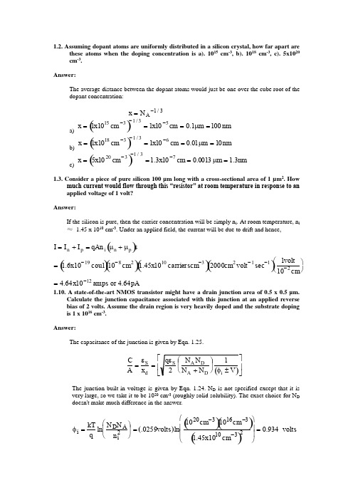
1.2. Assuming dopant atoms are uniformly distributed in a silicon crystal, how far apart arethese atoms when the doping concentration is a). 1015 cm -3, b). 1018 cm -3, c). 5x1020 cm -3.Answer:The average distance between the dopant atoms would just be one over the cube root of the dopant concentration:x =N A -1/3a)x =1x1015cm-3()-1/3=1x10-5cm =0.1μm =100nmb)x =1x1018cm-3()-1/3=1x10-6cm =0.01μm =10nmc)x =5x1020cm-3()-1/3=1.3x10-7cm =0.0013μm =1.3nm1.3. Consider a piece of pure silicon 100 µm long with a cross-sectional area of 1 µm2. Howmuch current would flow through this “resistor” at room temperature in response to an applied voltage of 1 volt?Answer: If the silicon is pure, then the carrier concentration will be simply n i . At room temperature, n i≈ 1.45 x 1010 cm -3. Under an applied field, the current will be due to drift and hence,I =I n +I p =qAn i μn +μp ()ε=1.6x10⁻¹⁹coul ()10-8cm 2()1.45x10¹⁰carrierscm -3()2000cm 2volt -1sec -1()1volt 10-2cm ⎛ ⎝ ⎫⎭=4.64x10⁻¹²amps or 4.64pA1.10. A state-of-the-art NMOS transistor might have a drain junction area of 0.5 x 0.5 µm.Calculate the junction capacitance associated with this junction at an applied reverse bias of 2 volts. Assume the drain region is very heavily doped and the substrate doping is 1 x 1016 cm -3. Answer:The capacitance of the junction is given by Eqn. 1.25.C A =εS x d =q εS 2N A ND N A +N D ⎛ ⎝ ⎫ ⎭ ⎪ 1φi ±V ()⎡ ⎣ ⎢⎤ ⎦ ⎥The junction built-in voltage is given by Eqn. 1.24. N D is not specified except that it is very large, so we take it to be 1020 cm -3 (roughly solid solubility). The exact choice for N D doesn't make much difference in the answer.φi =kT q ln N D N An i 2⎛ ⎝ ⎫ ⎭⎪ =.0259volt s ()ln 1020cm -3()1016cm -3()1.45x1010cm-3()2⎛ ⎝ ⎫⎭⎪ ⎪ =0.934 volt sSince N D >> N A in this structure, the capacitance expression simplifies toC A ≅εSW=qεS2N A()1φi±V()⎡⎣⎢⎤⎦⎥=1.6x10⁻¹⁹coul()11.7()1016cm-3()8.86x10⁻¹⁴Fcm-1()2()2.934volt s()⎡⎣⎢⎤⎦⎥ =1.68x10⁻⁸Fcm-2Given the area of the junction (0.25 x 10⁻⁸ cm2, the junction capacitance is thus 4.2 x 10⁻¹⁷ Farads.3.2. A boron-doped crystal pulled by the Czochralski technique is required to have aresistivity of 10 Ω cm when half the crystal is grown. Assuming that a 100 gm pure silicon charge is used, how much 0.01 Ω cm boron doped silicon must be added to the melt? For this crystal, plot resistivity as a function of the fraction of the melt solidified. Assume k 0 = 0.8 and the hole mobility µp = 550 cm 2 volt -1 sec -1.Answer:Using the mobility value given, and ρ=1q μN A we have:10 Ω cm ⇒ N A = 1.14 x 1015 cm -3 and 0.01 Ω cm ⇒ N A = 1.14 x 1018 cm -3From Eqn. 3.38, C S =C O k O 1-f ()k O -1and we want C S = 1.14 x 1015 cm -3 when f =0.5. Thus, solving for C 0 the initial doping concentration in the melt, we have:C 0=1.14x10150.81-0.5()0.2=1.24x1015cm -3But C 0=I 0V 0=# of impurities unit vol of melt =(Doping)(Vol. of 0.01 Ωcm)Vol 100 gm Si∴ Wgt added of 0.01 Ω cm S i = C 0Doping ⎛ ⎝ ⎫⎭ 100gm ()=0.109gmThe resistivity as a function of distance is plotted below and is given byρx ()=1q μN A x ()=1-f ()1-k 0q μC 0k 0=11.5Ωcm 1-f ()0.2R e s i s t i v i t y0.20.40.60.81Fraction Solidified - f3.3. A Czochralski crystal is pulled from a melt containing 1015 cm -3 boron and 2x1014 cm -3phosphorus. Initially the crystal will be P type but as it is pulled, more and more phosphorus will build up in the liquid because of segregation. At some point the crystal will become N type. Assuming k O = 0.32 for phosphorus and 0.8 for boron, calculate the distance along the pulled crystal at which the transition from P to N type takes place.Answer:We can calculate the point at which the crystal becomes N type from Eqn. 3.38 as follows:C S Phos ()=C 0k 01-f ()k 0-1=2x10¹⁴()0.32()1-f ()-0.68C S Boron ()=C 0k 01-f ()k 0-1=1015()0.8()1-f ()-0.2At the point where the cross-over occurs to N type, these two concentrations will be equal. Solving for f, we findf ≅0.995Thus only the last 0.5% of the crystal is N type.3.6. Suppose your company was in the business of producing silicon wafers for thesemiconductor industry by the CZ growth process. Suppose you had to produce the maximum number of wafers per boule that met a fairly tight resistivity specification. a). Would you prefer to grow N type or P type crystals? Why?b). What dopant would you use in growing N-type crystals? What dopant would you use in growing P type crystals? ExplainAnswer:a). Boron has the segregation coefficient closest to unity of all the dopants. Thus it produces the most uniform doping along the length of a CZ crystal. Thus P type would be the natural choice.b). For P type, the obvious (and only real choice) is boron as explained in part a). For N type crystals Fig. 3-18 shows that either P or As would be a reasonable choice since their segregation coefficients are quite close and are better than Sb. Table 3-2 indicates that P might be slightly preferred over As because its k O value is slightly closer to 1.4.1. An IC manufacturing plant produces 1000 wafers per week. Assume that each wafer contains 100 die, each of which can be sold for $50 if it works. The yield on these chips is currently running at 50%. If the yield can be increased, the incremental income is almost pure profit because all 100 chips on each wafer are manufactured whether they work or not. How much would the yield have to be increased to produce an annual profit increase of $10,000,000?Answer:At 1000 wafers per week, the plant produces 52,000 wafers per year. If each wafer has 50 good die each of which sells for $50, the plant gross income is simplyIncome = (52,000)(50)($50) = $130,000,000 per year.To increase this income by $10,000,000 requires that the yield increase by10130≅7.7%4.3. As MOS devices are scaled to smaller dimensions, gate oxides must bereduced in thickness.a. As the gate oxide thickness decreases, do MOS devices become more or lesssensitive to sodium contamination? Explain.b. As the gate oxide thickness decreases, what must be done to the substrate doping (oralternatively the channel V TH implant, to maintain the same V TH? Explain.Answer:a). From the text, Na+ contamination causes threshold voltage instabilities in MOS devices.Also from Eqn. 4.1, the threshold voltage is given byV TH=V FB+2φf+2εS qN A2φf()C OX+qQ MC OXAs the gate oxide thickness decreases, C OX increases, so the same amount of mobile charge Q M will have less effect on V TH as oxides get thinner. Therefore MOS devices are less sensitive to sodium contamination.b). Using the same expression for V TH as in part a), we observe that as the oxide thickness decreases, (C OX increases), to maintain the same V TH, N A will have to increase. N A willactually have to increase by the square root of the oxide thickness decrease to keep V TH constant.4.4. A new cleaning procedure has been proposed which is based on H2O saturated with O2as an oxidant. This has been suggested as a replacement for the H2O2 oxidizing solution used in the RCA clean. Suppose a Si wafer, contaminated with trace amounts of Au, Fe and Cu is cleaned in the new H2O/O2solution. Will this clean the wafer effectively?Why or why not? Explain.Answer:As described in the text, cleaning metal ions off of silicon wafers involves the following chemistry:M↔M z++ze-The cleaning solution must be chosen so that the reaction is driven to the right because this puts the metal ions in solution where they can be rinsed off. Since driving the reaction to the right corresponds to oxidation, we need an oxidizing solution to clean the wafer.H2O/O2 is certainly an oxidizing solution. But whether it cleans effectively or not depends on the standard oxidation potential of the various possible reactions. From Table 4-3 in the text, we have:The stronger reactions (dominating) are at the bottom.Thus the H2O/O2 reaction will clean Fe and Cu, but it will not clean Au off the wafer.4.5. Explain why it is important that the generation lifetime measurement illustrated inFigure 4-19 is done in the dark.Answer:The measurement depends on measuring carriers generated thermally in the silicon substrate (or at the surface). If light is shining on the sample, then absorbed photons can also generate the required carriers. As a result, the extracted generation lifetime with the light on would really be measuring the intensity of the incident light and not a basic property of the silicon material.5.1. Calculate and plot versus exposure wavelength the theoretical resolution and depth offocus for a projection exposure system with a NA of 0.6 (about the best that can be done today). Assume k 1 = 0.6 and k 2 = 0.5 (both typical values). Consider wavelengths between 100 nm and 1000 nm (DUV and visible light). ). Indicate the common exposure wavelengths being used or considered today on your plot (g-line, i-line, KrF and ArF). Will an ArF source be adequate for the 0.13 µm and 0.1 µm technology generations according to these simple calculations?Answer:The relevant equations are simply∴R =k 1λNA =0.6λ0.6 and DOF=±k 2λNA ()2=±0.5λ0.6()2These equations are plotted below. Note that the ArF (193 nm) will not reach 0.13 µm or 0.1 µm resolution according to these simple calculations. In fact, with more sophisticated techniques such as phase shift masks, off axis illumination etc., ArF is expected to reach 0.13 µm and perhaps the 0.1 µm generations.R e s o l u t i o n , D O F 祄20040060080010001200Exposure W avelength nm5.3. An X-ray exposure system uses photons with an energy of 1 keV. If the separation between the mask and wafer is 20 µm, estimate the diffraction limited resolution that is achievable by this system.Answer:The equivalent wavelength of 1 keV x-rays is given byE =h ν=hc λ∴ λ=hc E=4.14x10⁻¹⁵eVsec ()3x10¹⁰cmsec -1()103eV=1.24x10⁻⁷cm =1.24 nmX-ray systems operate in the proximity printing mode, so that the theoretical resolution is given by Eqn. 5.12:Resolut ion =λg =1.24x10⁻³μm ()20μm ()=0.15μm5.8. As described in this chapter, there are no clear choices for lithography systems beyondoptical projection tools based on 193-nm ArF eximer lasers. One possibility is an optical projection system using a 157-nm F 2 excimer laser.a. Assuming a numerical aperture of 0.8 and k 1 = 0.75, what is the expected resolution of such a system using a first order estimate of resolution?b. Actual projections for such systems suggest that they might be capable of resolving features suitable for the 2009 0.07 µm generation. Suggest three approaches to actually achieving this resolution with these systems.Answera). The simple formula for resolution isR =k 1λNA =0.750.157μm0.8=0.147μmb). The calculated resolution in part a is a factor of two larger than required for the 0.07 µm generation. Therefore some “tricks” will have to be used to act ually achieve such resolution. There are a number of possibilities:1. Use of phase-shift masks. This technique, discussed in this chapter, has the potential for significant resolution improvements. It works by designing a more sophisticated mask. Simple masks are digital - black or white. Phase shifting adds a second material to the mask features, usually at the edges which shifts the optical phase and sharpens up the aerial image. Sophisticated computer programs are required to design such masks.2. Use of optical proximity correction in the mask design. This is another approach to designing a better mask and as discussed in class, can also improve resolution significantly. The approach involves adding extra features to the mask, usually at corners where features are sharp, to compensate for the high frequency information lost to diffraction effects.3. Off-axis illumination. This allows the optical system to capture some of the higher order diffracted light and hence can improve resolution.5.9. Current optical projection lithography tools produce diffraction limited aerial images. A typical aerial image produced by such a system is shown in the simulation below where a square and rectangular mask regions produce the image shown. (The mask features are the black outlines, the calculated aerial image is the grayscale inside the black rectangles.) The major feature of the aerial image is its rounded corners compared to the sharp square corners of the desired pattern. Explain physically why these features look the way they do, using diffraction theory and the physical properties of modern projection optical lithography tools.Answer:Modern optical projection lithography systems are limited in the resolution they can achieve by diffraction effects. The finite size of the focusing lens means that the high order diffraction components are “lost” and are therefore not available to help in printing a replica of the mask image. But the high frequency spatial components are exactly the components that contain information about “sharp” features, i.e. corners etc. Thus the projected aerial image loses this information and corners become rounded. The only ways to improve the image are by using shorter wavelength light, or a higher NA lens.5.10. Future optical lithography systems will likely use shorter exposure wavelengths toachieve higher resolution and they will also likely use planarization techniques to provide “flat” substrates on which to expose the resist layers. Explain why “flat”substrates will be more important in the future than they have been in the past. Answer:As the wavelength of the exposure system decreases, the depth of focus of the exposure system also decreases. Thus it will be necessary to make sure that the resist in which the image is to be exposed, is flat and does not require much depth of focus. Planarization techniques will be required to accomplish this. This could mean CMP to planarize the substrate before the resist is applied, or it could mean using a spun on resist which planarizes the substrate and which is then covered with a thin, uniform imaging resist layer.6.4. Construct a HF CV plot for a P-type silicon sample, analogous to Fig. 6-9. Explain your plot based on the behavior of holes and electrons in the semiconductor in a similar manner to the discussion in the text for Fig. 6.9. Answer:C ODV GGQ GQ IQ DThe C-V plot looks basically the same as the N substrate example in the text, that we discussed in class, except that the horizontal axis is flipped. For negative applied gate voltages, the majority carrier holes in the substrate are attracted to the surface. This is the accumulation region a) above. We measure just C OX for the capacitance since there is no depletion in the substrate. For + V G, the holes are driven away from the surface creating first a depletion region as in b) and finally an inversion layer of electrons as in c). Themeasured capacitance drops as we move into depletion and finally reaches a minimum value after an inversion layer forms.The C-V curves shown are high frequency curves. As discussed in the text, the capacitance remains at its minimum value for + V G values greater than V TH because the inversion layer electrons cannot be created or destroyed as fast as the signal is changing. Hence the small AC signal must “wiggle” the bottom of the depletion region to balance ∆V G.6.6. In a small MOS device, there may be a statistical variation in V T due to differences inQ F from one device to another. In a 0.13 µm technology minimum device (gate oxide area = 0.1µm x 0.1µm) with a 2.5nm gate oxide, what would the difference in threshold voltage be for devices with 0 or 1 fixed charge in the gate oxide?Answer:The oxide capacitance isC ox=εAd=3.9⨯8.854⨯10-14()0.1⨯10-4()0.1⨯10-4()2.5⨯10-7=1.38⨯10-16The change in threshold voltage is given by∆V T=qQ FC ox=1.6⨯10-19()1()1.38⨯10-16=1.1mVThis shows that a single electron trap in a gate oxide will have a negligible effect on thethreshold voltage at this technology generation.6.12 A silicon wafer is covered by an SiO2 film 0.3 μm thick.a. What is the time required to increase the thickness by 0.5 μm by oxidation in H2Oat 1200˚C?b. Repeat for oxidation in dry O2at 1200˚C.Answer:We will perform the calculation for <111> silicon wafers. For <100> wafers, the linear rate constant should be divided by 1.68.a. At 1200˚C, in H2OB=3.86⨯102exp-0.78 kT⎛ ⎝ ⎫⎭ =0.829μm2/hrB A =1.63⨯108exp-2.05kT⎛⎝⎫⎭ =15.86μm/hrA=0.052μmThe initial oxide, if grown at 1200˚C would have taken this long to growτ=x i2+Ax iB=0.3()2+0.052()0.3()0.829=0.127hrThe time required to grow 0.8μm at 1200˚C isτ=x i 2+Ax i B =0.8()2+0.052()0.8()0.829=0.822hrThus, the time required to add 0.5μm to an existing 0.3μm film is0.822-0.127=0.695hr or 41.7 minutes.b. At 1200˚C, in dry oxygenB =7.72⨯102exp - 1.23k(1200+273)⎛ ⎝ ⎫ ⎭ =0.048μm 2/hrB A =6.23⨯106exp -2.0kT ⎛ ⎝ ⎫ ⎭ =0.899μm /hrA =0.053μmThe initial oxide would have taken 2.206 hours to grow in dry oxygen, it would require 14.217 hours to grow 0.8μm , thus would require an additional 12 hours to add 0.5μm to an existing 0.3μm film.6.13. Suppose an oxidation process is used in which (100) wafers are oxidized in O 2 for threehrs. at 1100˚C, followed by two hrs. in H 2O at 900˚C, followed by two hrs in O 2 at 1200˚C. Use Figs. 6-19 and 6-20 in the text to estimate the resulting final oxide thickness. Explain how you use these figures to calculate the results of a multi-step oxidation like this.Answer:We can use these figures to estimate the oxide thickness as follows. First, we use Fig. 6-19 for the first dry oxidation cycleA three hour oxidation at 1100˚C produces an oxide thickness of about 0.21 µm. We nextuse Fig. 6-20 for the wet oxidation as shown below. The oxidation is 2 hrs in H 2O at 90 ˚C. We start by finding the point on the 900˚C curve that corresponds to 0.21 µm since this is the starting oxide thickness. This is point A. We then move along the 900˚C curve by two hours to point B. This corresponds to a thickness of about 0.4 µm which is the thickness at the end of the wet oxidation.We now go back to Fig. 6-19 for the final dry O 2 cycle. This process is 2 hrs at 1200˚C. Westart by finding the point on the 1200˚C curve that corresponds to a starting oxide thickness of 0.4 µm. This is point A below. We then increment the time by 2 hrs along the 1200˚C curve, to arrive at a final oxide thickness of about 0.5 µm.6.18. Silicon on Insulator or SOI is a new substrate material that is being considered forfuture integrated circuits. The structure, shown below, consists of a thin single crystal silicon layer on an insulating (SiO 2) substrate. The silicon below the SiO 2 provides mechanical support for the structure. One of the reasons this type of material is being considered, is because junctions can be diffused completely through the thin silicon layer to the underlying SiO 2. This reduces junction capacitances and produces faster circuits. Isolation is also easy to achieve in this material, because the thin Si layer can be completely oxidized, resulting in devices completely surrounded by SiO 2. A LOCOS process is used to locally oxidize through the silicon as shown on the right below. Assuming the LOCOS oxidation is done in H 2O at 1000˚C, how long will it take to oxidize through the 0.3 µm silicon layer? Calculate a numerical answer using the Deal Grove model.Answer:To oxidize completely through a 0.3 µm silicon layer, we will need to grow (2.2)(0.3 µm) = 0.66 µm of SiO 2. At 1000˚C in H 2O, the Deal Grove rate constants are given by (Table 6-2):B =3.86x10²exp -0.78eV kT ⎛ ⎝ ⎫ ⎭ =0.316μm 2hr-1B A =1.63x1081.68exp -2.05eV kT ⎛ ⎝ ⎫ ⎭ =0.747μmhr -1∴t =0.66()20.316+0.660.747≅2.25 hours6.23. As part of an IC process flow, a CVD SiO 2 layer 1.0 µm thick is deposited on a <100>silicon substrate. This structure is then oxidized at 900˚C for 60 minutes in an H 2O ambient. What is the final SiO 2 thickness after this oxidation? Calculate an answer, do not use the oxidation charts in the text .Answer:At 900˚C in H 2O, the oxidation rate constants are given by:B =3.86x10²exp -0.788.62x10-5()1173()⎛ ⎝ ⎫ ⎭ ⎪ μm 2 hr -1=0.17 μm 2 hr -1B A =1.63x1081.68exp - 2.058.62x10-5()1173()⎛ ⎝ ⎫ ⎭ ⎪ μm hr -1=0.152 μm hr -1The initial oxide on the wafer is 1.0 µm thick. This corresponds to a τ ofτ=1()2+1()0.170.152⎛ ⎝⎫⎭ 0.17=12.46 hoursThus the final oxide thickness is given byx o =0.172()0.152()1+13.461.11()24()0.17()-1⎧ ⎨ ⎪ ⎩ ⎪ ⎫⎬ ⎪ ⎭ ⎪=1.064 μmThus not much additional oxide grows.Chapter 7 Problems7.1. A resistor for an analog integrated circuit is made using a layer of deposited polysilicon0.5 µm thick, as shown below.Polysilicon (a) (a) The doping the polysilicon is 1⨯10 cm -3. The carrier mobilityμ=100cm 2V -1sec -1is low because of scattering at grain boundaries. If the resistor has L=100µm, W=10µm, what is its resistance in Ohms?(b) (b) A thermal oxidation is performed on the polysilicon for 2 hours at 900˚C inH 2O . Assuming B/A for polysilicon is 2/3 that of <111> silicon, what is thepolysilicon thickness that remains.(c) (c) Assuming that all of the dopant remains in the polysilicon (i.e. does notsegregate to oxide), what is the new value of the resistor in (a). Assume the mobility does not change.Answer:(a)ρ=1nq μ=11⨯1016()1.6⨯10-19()100()=6.25ΩcmρS =ρx j = 6.250.5⨯10-4=125k ΩR =10010ρS =1.25M Ω(10squares)(b) The linear rate coefficient at 900˚C isB A ⎛ ⎝ ⎫ ⎭ poly =23 1.63⨯108exp -2.05kT ⎛ ⎝ ⎫ ⎭ ⎛ ⎝ ⎫ ⎭=0.170μm hr-1The parabolic rate constant for poly is unchanged:B pol y =3.86⨯102exp -0.78kT ⎛ ⎝ ⎫ ⎭ =0.172μm 2hr-1A poly =1.01μmThe oxide thickness isx o =A 21+tA 2/4B -1⎧ ⎨ ⎩ ⎫ ⎬⎭x o =1.0121+21.01()2/40.172()-1⎧ ⎨ ⎩ ⎫ ⎬ ⎭ =0.27μmThis oxide consumes a silicon thickness of 0.45*0.27=0.12 µm, leaving a remaining polysilicon thickness of 0.5-0.12=0.38 µm and contains all the dopant with a concentration of1⨯1016()0.50.38=1.31⨯1016cm -3(c) Since the concentration has gone up and the thickness has gone down by the same factor, the polysilicon restivity and hence the resistance of the line remains the same.7.4. Suppose we perform a solid solubility limited predeposition from a doped glass sourcewhich introduces a total of Q impurities / cm 2.(a) (a) If this predeposition was performed for a total of t minutes, how long would ittake (total time) to predeposit a total of 3Q impurities / cm 2 into a wafer if the predeposition temperature remained constant.(b) (b) Derive a simple expression for the Dt ()drive -in which would be required todrive the initial predeposition of Q impurities / cm 2 sufficiently deep so that the final surface concentration is equal to 1% of the solid solubility concentration. Thiscan be expressed in terms ofDt ()predep and the solid solubility concentrationC S .Answer:(a)Q =2C SπDt ⇒Q ∝t∴3Q ⇒9t(b)C 0,t ()drive -in =QπDt =0.01C SQ =2C SπDt ()predep∴2πDt ()predep Dt ()drive -in=0.01∴Dt ()drive -in =200π⎛ ⎝ ⎫⎭ 2Dt ()predep7.7. A boron diffusion is performed in silicon such that the maximum boron concentration is1 x 1018 cm -3. For what range of diffusion temperatures will electric field effects and concentration dependent diffusion coefficients be important?Answer:Electric field effects and concentration dependent diffusion are both important when the doping concentration exceeds the intrinsic electron (or hole) concentration. The intrinsic orbackground electron concentration is n i which increases with higher temperature. This provides a background sea of electrons or holes in the lattice at a given temperature. If the doping exceeds this concentration, then these extrinsic effects are important.When the temperature is below the temperature where n i =1⨯1018/cm 3, these effects will become dominant since they often depend on n /n i (where n =N A or n =N D to a first approximation).n i =3.9⨯1016T 32exp -0.605kT⎛ ⎝ ⎫ ⎭By trial and error, n i =1⨯1018/cm 3at T=720C.Therefore, extrinsic effects become important below 720˚C.7.15. A silicon wafer is uniformly doped with boron (2 x 1015 cm -3) and phosphorus (1 x 1015cm -3) so that it is net P type. This wafer is then thermally oxidized to grow about 1 µm of SiO 2. The oxide is then stripped and a measurement is made to determine the doping type of the wafer surface. Surprisingly it is found to be N type. Explain why the surface was converted from P to N type. Hint: Consider the segregation behavior of dopants when silicon is oxidized.Answer:The boron segregates preferentially into the growing oxide, thus depleting the surface concentration in the silicon. The phosphorus on the other hand preferentially segregates (piles-up) on the silicon side of the interface. Both of these effects act in the same direction and tend to make the surface of the silicon more N-type.It is for this reason that a P-type “channel stop” implant is almost always needed under a locally oxidized lightly doped P-type region, to prevent depletion of the P-type dopant in the substrate and in the worst case to prevent an N-type channel from forming.7.20. Fig. 7.38 shows that a wet oxidation produces a significantly higher C I /C I *than doesa dry O 2 oxidation. Explain quantitatively why this should be the case. Answer:BecauseC I ∝dx dta faster oxidation rate produces a higher interstitial supersaturation. Thus, wet oxidationproduces a higher C I /C I *than dry oxidation, for the same time at the same temperature.Chapter 8 Problems8.1. Arsenic is implanted into a lightly doped p-type Si substrate at an energy of 75keV . Thedose is 1⨯1014/cm 2. The Si substrate is tilted 7˚ with respect to the ion beam to make it appear amorphous. The implanted region is assumed to be rapidly annealed so that complete electrical activation is achieved. What is the peak electron concentration produced?Answer:From Fig. 8-3, the range and standard deviation for 75 keV arsenic areR P =0.05μm ∆R P =0.02μmThe peak concentration isC P =Q2π∆R P=1⨯10142π0.02⨯10-4()=2⨯1019cm -3Assuming all the dose is active, then the peak electron concentration is equal to the peak dopant concentration.8.4. How thick does a mask have to be to reduce the peak doping of an implantby a factor of 10,000 at the mask/substrate boundary. Provide an equation in terms of the Range and the Standard Deviation of the implant profile.Answer:We want to reduce the peak doping N P *in the mask at range R P *by 10,000 at the mask/substrate boundary. We will use the equation which describes the profile of an implant in a mask layerN *(d)=N P *exp -d -R P*()22∆R P *2⎡ ⎣ ⎢ ⎢ ⎤ ⎦⎥ ⎥WhenN *(d)N P *=10-4we haved =R P *+4.3∆R P *8.6. The equations below provide a reasonable analytical description for some of thediffusion processes indicated schematically in the diagrams on the following page. Put the equation number (a-f) on each figure that is the best match. Equations may be。
大规模集成电路与超大规模集成电路
大规模集成电路与超大规模集成电路
随着电子科技的不断发展,集成电路得到了极大的发展与进步,其中包括了大规模集成电路(Large Scale Integration, LSI)和超大规模集成电路(Very Large Scale Integration, VLSI)。
首先来介绍一下大规模集成电路。
大规模集成电路是指将上千个晶体管、电容、电阻等离散元器件集成到一块硅片上,从而产生一个功能完整的电路系统。
使用大规模集成电路,能够大幅度降低电路成本、体积和功耗,提升系统性能和可靠性,因此在计算机、电信、工业自动化等领域得到了广泛应用。
而VLSI则更加高级和复杂,它所集成的晶体管数量比大规模集成电路还要多,一般超过了10万个,甚至可以达到数千万或更多的晶体管数量。
因此,VLSI要求制造工艺更加精密和先进,也需要更高的设计和布局能力。
VLSI广泛应用于高速通讯、人工智能、计算机芯片、超级计算机等领域。
总体来说,LSI和VLSI同样具有极高的集成度和可靠性,并提供了更强大的系统性能和更高的效率。
他们的不同之处在于,VLSI要求更高的技术要求和更复杂的设计,因此适用于更多的高端技术领域。
值得注意的是,虽然LSI和VLSI在大多数领域中具有广泛应用,但是还存在着一些技术瓶颈,如制造成本和技术难度等需要不断攻克。
因此,随着电子科技的不断发展和迭代,新的集成电路技术和应用也将不断涌现。
总之,集成电路的发展已经成为电子科技领域的重要标志之一。
LSI和VLSI代表了集成电路技术的顶峰,二者的发展都在推动科技进步和人类文明的发展。
超大规模集成电路的设计与制造技术
超大规模集成电路的设计与制造技术第一章:引言随着现代数字电子技术的飞速发展,超大规模集成电路(VLSI)的设计和制造技术已经成为了电子领域内的重要课题。
VLSI 代表了现代电子技术中的一个重要里程碑,在计算机科学、通信工程、嵌入式系统等课题中都有着广泛应用。
本文将讨论超大规模集成电路的概念及其设计与制造技术。
第二章:超大规模集成电路的概念VLSI 是指将数千万甚至数亿个晶体管和双极性器件集成到单个芯片上的技术。
随着设备的不断发展,集成电路规模的扩大和技术的更新换代,超大规模集成电路已经从过去的 10 万门电路乃至几百万门电路发展到现在的千万门电路。
超大规模集成电路实现了芯片功能的高度集成和小型化,大幅度提高了芯片的可靠性和集成度,降低了生产成本,提高了芯片的性能。
第三章:超大规模集成电路的设计技术超大规模集成电路的设计技术主要涉及到电子设计自动化(EDA)工具的开发。
EDA 工具是一类能够自动完成电路设计流程的软件系统,主要包括原理图输入、电路仿真、自动布线、物理布局等功能。
通过EDA 工具,可以高效地完成芯片设计和优化。
超大规模集成电路的设计过程涉及到原理图输入、功能仿真、逻辑合成、门级设计、布图设计、物理设计等步骤。
其中,原理图输入是指将电路的逻辑设计手绘出来,以电路图的方式进行输入。
功能仿真是指在计算机上对电路进行模拟并确认电路功能的正确性。
逻辑合成是将设计好的原理图转成可综合的门级电路。
门级设计将逻辑合成的电路变换成另一种级别的门级电路。
布图设计是将门级电路转换为物理电路图。
物理设计是根据物理约束将各个单元摆放好位置。
此外,超大规模集成电路的设计还需要考虑功耗、时序、容错、可测试性等方面因素,以保证芯片在运行过程中的可靠性和性能。
第四章:超大规模集成电路的制造技术超大规模集成电路的制造过程主要分为光刻、蚀刻、离子注入、热处理、载带加工、封装等步骤。
在芯片制造的过程中,需要采用微纳加工技术,进行复杂的加工过程,以实现制造复杂电路。
硅超大规模集成电路工艺技术

硅超大规模集成电路工艺技术硅超大规模集成电路工艺技术是现代电子科技领域中的重要一环,它的发展对于电子产品的性能提升、功耗降低以及体积的缩小有着重要的影响。
硅超大规模集成电路工艺技术的核心是利用硅材料进行器件制造和集成,通过多种工艺步骤将各种电子元件(晶体管、电容器等)集成到硅芯片上,形成复杂的电路结构。
而工艺技术的发展则主要包括制作技术、工艺流程、材料研发等方面。
在硅超大规模集成电路工艺技术中,首先要解决的是超大规模集成电路的制造问题。
由于集成的器件数量巨大,器件之间存在非常紧密的空间,因此制造工艺需要高度精准。
制造技术的发展主要包括光刻技术、薄膜沉积技术、离子注入技术等,其中光刻技术是非常关键的一个环节,它可以通过光的干涉和投影的方式将芯片上的图形投射到硅片上,从而形成电路结构。
其次,硅超大规模集成电路工艺技术还需要解决的是工艺流程的设计问题。
工艺流程是整个制造工艺中的一个重要环节,它涉及到各个工艺步骤的顺序、时间和温度等参数的控制。
合理的工艺流程可以提高产能、降低成本,并且也对芯片的性能和可靠性有着直接的影响。
因此,人们通过工艺优化和新材料的应用来改善工艺流程,以提高电路的性能。
最后,硅超大规模集成电路工艺技术还需要研究新的材料以及器件结构的设计。
目前,人们已经发展了多种新材料,例如高介电常数材料、金属电极材料等,以满足电路中对高速信号传输和功耗降低的需求。
而在器件结构方面,人们通过改变晶体管的形状和尺寸等参数,实现了更好的电流控制和更低的功耗。
总的来说,硅超大规模集成电路工艺技术的发展为电子产品的性能提升和体积缩小提供了重要的支持。
通过不断地研究和改进,人们相信硅超大规模集成电路工艺技术将会进一步发展,为人们的生活带来更多的便利。
硅集成电路工艺简介
负胶:分辨率差,适于加工线宽≥3m的
线条
几种常见的光刻方法
接触式光刻、接近式曝光、投影式曝光
光学曝光的各种曝光方式及其利弊
接成品率低。
优点:掩模版寿命长,成本低。
接近式
非
缺点:衍射效应严重,影响分辨率。
接
优点:无像差,无驻波效应影响。
D
G
S
G
D
S
Al
SiO2
N
N
P-si
掺杂:将需要的杂质掺入特定的 半导体区域中,以达到改变半导 体电学性质,形成PN结、电阻、 欧姆接触
磷(P)、砷(As) — N型硅
硼(B) — P型硅
掺杂工艺:扩散、离子注入
扩散
替位式扩散:杂质离子占据硅原子的位:
– Ⅲ、Ⅴ族元素 – 一般要在很高的温度(950~1280℃)下进行,
蚀。具有溅射刻蚀和等离子刻蚀两者的优点,同 时兼有各向异性和选择性好的优点。目前,RIE 已成为VLSI工艺中应用最广泛的主流刻蚀技术。
2.3 掺杂工艺(扩散与离子注入)
通过掺杂可以在硅衬底上形成不同类型的半导体区
域,构成各种器件结构。掺杂工艺的基本思想就是通过 某种技术措施,将一定浓度的Ⅲ价元素,如硼,或Ⅴ价 元素,如磷、砷等掺入半导体衬底。
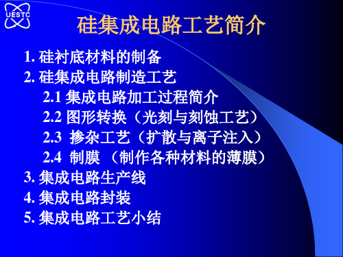
2. 集成电路制造工艺
2.1 集成电路加工过程简介
一、硅片制备(切、磨、抛)
*圆片(Wafer)尺寸与衬底厚度: 3— 0.4mm 5— 0.625mm 4— 0.525mm 6— 0.75mm
硅片的大部分用于机械支撑。
晶圆退火工艺流程
晶体生长
Crystal Growth
硅晶体
Si Crystal
- 1、下载文档前请自行甄别文档内容的完整性,平台不提供额外的编辑、内容补充、找答案等附加服务。
- 2、"仅部分预览"的文档,不可在线预览部分如存在完整性等问题,可反馈申请退款(可完整预览的文档不适用该条件!)。
- 3、如文档侵犯您的权益,请联系客服反馈,我们会尽快为您处理(人工客服工作时间:9:00-18:30)。
Academic Qualification:
The main research field is Nano Material, Novel Micro/Nano-electronic Devices, Design and Process of Semiconductor Chip. In recent years, she has been responsible for more than ten research funds from NSFC, 863, and Hubei Province. She published more than 70 papers and applied more than 20 patents. She is the memberof the semiconductor materials and Equipment Standardization Technical Committee.
光学与电子信息
课程名称:硅超大规模集成电路工艺技术
课程代码:182.558
课程类型:□公共课□专业必修课█专业课程□其它:
考核领域:考试
教学方式:讲授
适用领域:集成电路工程、软件工程
开课学期:春季
总学时:32
学分:2
先修课程要求:半导体物理/固体物理半导体器件
课程组教师姓名
职称
专业
年龄
学术方向
周文利
第七章薄膜淀积
7.1物理气相淀积
7.2化学气相淀积
第八章刻蚀
8.1湿法腐蚀
8.2等离子刻蚀
8.3反应离子刻蚀
第九章后端工艺
9.1平坦化
9.2互联
第十章工艺集成—现代CMOS工艺
教材:
《硅超大规模集成电路工艺技术:理论、实践、与模型》
【美】普卢默等著,严利人等译(电子工业出版社,第一版)
主要参考书:
《微电子制造科学原理与工程技术》(电子工业出版社,第二版)来自教授微电子学与固体电子学
45
半导体芯片设计与工艺
陈实
副教授
微电子学与固体电子学
46
薄膜传感器与智能系统
课程负责教师教育经历及学术成就简介:
教育经历:
1986年9月至1990年7月,华中工学院检测技术与仪器专业,本科生
1992年9月至1995年7月,华中理工大学半导体器件与微电子学专业,硕士研究生
2000年10月至2004年1月,香港中文大学自动化与计算机辅助工程专业,博士研究生
45
Design and process of semiconductor Chip
Course Team Leader Education Experience and Academic Qualification:
Education Experience:
Sep,1986-July,1990 Huazhong Institute of Technology, Measurement Technology and Instrumentation Bachelar Degree
.
课程名称:Silicon VLSI Process Technology
课程代码:182.558
课程类型:█ Major Basics
考核方式:Exam
教学方式:Lecturing
适用领域:Integrated Circuit Engineering,Software Engineering
开课学期:Spring
总学时:32
学分:2
先修课程要求:Semiconductor Physics/ Solid States Physics, Semiconductor Devices
课程组教师姓名
职称
专业
年龄
学术方向
Zhou Wenli
Prof.
Microelectronics and solid state electronics
2004年3月至2005年9月,香港中文大学博士后
学术成就:
主要从事纳米材料、新型微纳电子器件和半导体芯片设计与工艺等领域的研究工作。近几年来先后主持、参与承担了十多项国家自然科学基金、国家863计划、湖北省自然科学基金、科技攻关等科研项目。具有较高的学术水平和丰富的科研工作经验。在国内外期刊和学术会议上发表和与人合作发表论文逾70篇;申请专利和集成电路布图设计专有权20余项。担任全国半导体材料与设备标准化技术委员会委员。
【美】Stephen A. Campbell著,曾莹,严利人,王纪民等译
《硅集成电路工艺基础》关旭东编著,北京大学出版社, 2004
《微加工导论》陈迪等译,电子工业出版社, 2006
《超大规模集成电路工艺原理》——硅和砷化镓S.K甘地著章熙康等译
《集成电路工艺基础》王阳元等著
考核方式:
开卷考试或报告占70%,平时作业和考勤占30%。
课程教学目标:
本课程以学习硅超大规模集成电路芯片生产制造的实际工艺技术为主。学生将重点掌握各项工艺技术的科学原理、工艺模型及测量方法,并了解各项工艺技术与工艺模型的未来发展趋势,从而具备进行微电子器件和集成电路工艺设计的能力。
课程大纲:(章节目录)
第一章绪论
第二章晶体生长、晶圆片制造与硅原片的基本特性
2.1晶体生长方法与设备
2.2晶体结构与缺陷硅中的氧硅中的碳
2.3测量方法
第三章半导体制造
3.1超净室
3.2晶圆片清洗
3.3吸杂处理
第四章光刻
4.1曝光系统
4.2光刻胶
4.3先进光刻技术
第五章热氧化与Si-SiO2界面
5.1氧化动力学
5.2 Si-SiO2界面
第六章扩散与离子注入
6.1扩散
6.2离子注入
Chen Shi
Assoc. Prof.
Sep,1992-July,1995 Huazhong University of Science and Technology, Semiconductor Device and Microelectronics Master Degree
Oct,2000-Jan,2004 The Chinese University of Hongkong, Automation and Computer-aided Engineering Ph.D. Degree