FPGA可编程逻辑器件芯片XC2S100-5TQG144C中文规格书
FPGA可编程逻辑器件芯片XC2S30-5FG456C中文规格书
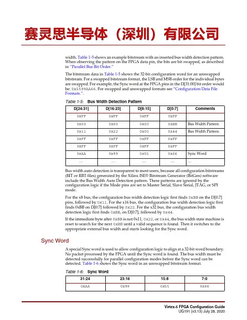
width. Table 1-5 shows an example bitstream with an inserted bus width detection pattern.When observing the pattern on the FPGA data pin, the bits are bit swapped, as describedin “Parallel Bus Bit Order.”The bitstream data in Table 1-5 shows the 32-bit configuration word for an unswappedbitstream. For a swapped bitstream format, the LSB and MSB order for the individual bytesare swapped. For example, the Sync word at the FPGA pins in the D[31:00] bit order wouldbe: 0x5599AA66. For swapped and unswapped formats see “Configuration Data FileFormats.”.Bus width auto detection is transparent to most users, because all configuration bitstreams(BIT or RBT files) generated by the Xilinx ISE® Bitstream Generator (BitGen) softwareinclude the Bus Width Auto Detection pattern. These patterns are ignored by theconfiguration logic if the Mode pins are set to Master Serial, Slave Serial, JTAG, or SPImode.For the x8 bus, the configuration bus width detection logic first finds 0xBB on the D[0:7]pins, followed by 0x11. For the x16 bus, the configuration bus width detection logic firstfinds 0xBB on D[0:7] followed by 0x22. For the x32 bus, the configuration bus widthdetection logic first finds 0xBB , on D[0:7], followed by 0x44.If the immediate byte after 0xBB is not 0x11, 0x22, or 0x44, the bus width state machine isreset to search for the next 0xBB until a valid sequence is found. Then it switches to theappropriate external bus width and starts looking for the Sync word.Sync WordA special Sync word is used to allow configuration logic to align at a 32-bit word boundary.No packet processed by the FPGA until the Sync word is found. The bus width must bedetected successfully for parallel configuration modes before the Sync word can bedetected. Table 1-6 shows the Sync word in an unswapped bitstream format.Table 1-5:Bus Width Detection Pattern D[24:31]D[16:23]D[8:15]D[0:7]Comments0xFF0xFF 0xFF 0xFF 0x000x000x000xBB Bus Width Pattern 0x110x220x000x44Bus Width Pattern0xFF 0xFF 0xFF 0xFF 0xFF0xFF 0xFF 0xFF 0xAA0x990x550x66Sync Word ……………Table 1-6:Sync Word31:2423:1615:87:00xAA 0x990x550x66Generating PROM FilesChapter 2:Configuration Interfaces∙Sending a bitstream to the data pin follows the same bit-swapping rule as in SelectMAP mode. See “Parallel Bus Bit Order.”∙If Flash programming is not required, FCS_B, FOE_B, and FWE_B can be tied off; that is, DONE is connected to FCS_B, FOE_B is tied Low, and FWE_B is tied High.∙The CCLK outputs are not used to connect to Flash but are used to sample Flash readdata during configuration. All timings are referenced to CCLK. The CCLK pin mustnot be driven or tied High or Low.∙The RS[1:0] pins are not connected as shown in Figure 2-22. These output pins areonly required for MultiBoot configuration. See Chapter 8, “Reconfiguration andMultiBoot.”∙HSWAPEN must be connected to either disable or enable the pull-up resistors.∙If HSWAPEN is left unconnected or tied High, a pull-up resistor is required forFCS_B.∙If HSWAPEN is tied Low, the FCB_B, FOE_B, FWE_B, and the address pins haveinternal weak pull-up resistors during configuration. After configuration, FCS_B canbe either controlled by I/O in user mode or by enabling a weak pull-up resistorthrough constraints.∙To enable the active driver on DONE, the DriveDONE option in BitGen must beenabled.∙“MultiBoot Bitstream Spacing,” page 155 provides information on when DCI or DCMlock wait is turned on.∙For daisy chaining FPGAs in BPI mode, see Figure 2-12, page 52.∙The BPI Flash vendor data sheet should be referred to for details on the specific Flashsignal connectivity. To prevent address misalignment, close attention should be paidto the Flash family address LSB for the byte/word mode used. Not all Flash familiesuse the A0 as the address LSB.Table 2-9 defines the BPI configuration interface pins.If the FPGA is subject to reprogramming or fallback during configuration from the BPIflash, then the INIT pin can be connected to the BPI reset to set the BPI into a known state.Table 2-9:Virtex-5 Device BPI Configuration Interface Pins Pin Name TypeDedicated or Dual-PurposeDescription M[2:0] Input Dedicated The Mode pins determine the BPI mode:010 = BPI-Up mode011 = BPI-Down modeHSWAPEN Input Dedicated Controls I/O (except Bank 0 dedicated I/Os) pull-up resistors duringconfiguration. This pin has a built-in weak pull-up resistor.0 = Pull-up during configuration1 = 3-state during configurationDONE Bidirectional, Open-Drain, or Active Dedicated Active-High signal indicating configuration is complete:0 = FPGA not configured 1 = FPGA configuredByte Peripheral Interface Parallel Flash Mode INIT_B Input or Output, Open-Drain Dedicated Before the Mode pins are sampled, INIT_B is an input that can be heldLow to delay configuration. After the Mode pins are sampled, INIT_Bis an open-drain, active-Low output indicating whether a CRC erroroccurred during configuration:0 = CRC error1 = No CRC errorWhen the SEU detection function is enabled, INIT_B is optionallydriven Low when a read back CRC error is detected.PROGRAM_B Input Dedicated Active-Low asynchronous full-chip resetCCLK Output Dedicated Configuration clock output. CCLK does not directly connect to BPIFlash but is used internally to generate the address and sample readdata.FCS_B Output Dual Active-Low Flash chip select output. This output is actively driven Lowduring configuration and 3-stated after configuration. It has a weakpull-up resistor during configuration. By default, this signal has a weakpull-down resistor after configuration.FOE_B Output Dual Active-Low Flash output enable. This output is actively driven Lowduring configuration and 3-stated after configuration. It has a weakpull-up resistor during configuration. By default, this signal has a weakpull-down resistor after configuration.FWE_B Output Dual Active-Low Flash write enable. This output is actively driven Highduring configuration and 3-stated after configuration. It has a weakpull-up resistor during configuration. By default, this signal has a weakpull-down resistor after configuration.ADDR[25:0]Output DualAddress output. For I/O bank locations, see Table 1-2, page 17.D[15:0]Input Dual Data input, sampled by the rising edge of the FPGA CCLK. For I/Obank location, see Table 1-2, page 17.Table 2-9:Virtex-5 Device BPI Configuration Interface Pins (Continued)Pin NameType Dedicated or Dual-Purpose DescriptionChapter 2:Configuration Interfaces。
FPGA可编程逻辑器件芯片XC3S100E-5FGG484C中文规格书
Chapter 9Programmable LogicThe programmable logic (PL) is a scalable structure that provides the ability to create manypossible functions. The PL logic regions include DSP engines, configurable logic blocks, and two types of RAM arrays. These are configured together to create almost any type of hardwarefunctionality including accelerators, processors, functional pipeline units, and peripherals. The PL includes connections for the integrated hardware and peripherals, ports to the NoC interconnect,access to CMOS and gigabit high-speed I/O, and interface channels to the PS.The PL complements the functionality of the PS, AI Engine, and other integrated hardware to improve application performance. The PL instantiates system functionality and provides connectivity between the system and integrated hardware and peripherals.The PMC and PS have many signal connections and bus interfaces to the PL. These aresummarized in the Boundary Interface Signals chapter.PL ConfigurationThe connections and configuration of the PL elements are captured in the Vivado ® design suite and the Vitis ™ unified software platform tool chain using a programmable device image (PDI).The PDI contains PL configuration frames (CFRAME), which are sent by the PLM to theconfiguration frame unit (CFU) for processing. The CFU interfaces to the PL via the configuration frame interface (CFI). The PL can be configured during the boot process and can be re-configured during normal system operation. The PL configuration can be read-back for debug and functional safety applications. The CFU is described in Configuration Frame Unit and the CFI is described in Configuration Frame Interface .Building BlocksThe PL includes building blocks and provides several types of connections to many parts of the device including several subsystems and I/O. The PL has AXI interfaces to the PS, CPM, AI Engine, and the integrated controllers. The PL also has port interface signals and parameter configuration inputs to the PS, PMC, and other parts of the system.The PL building blocks include the DSP Engine, configurable logic block (CLB), Block RAM, and UltraRAM integrated components. These components are surrounded by clocking structures and wiring pathways. The PL makes connection between PS, CPM, PMC, NoC, AI Engine, GTs, XPIO banks, high-density I/O (HDIO) buffers, and components instantiated within the PL.The PL building blocks include:Section II: Hardware ArchitectureChapter 9: Programmable LogicAM011 (v1.1) November 30, 2020Versal ACAP TRM○ULPI is routed via the PMC MIO (not LPD MIO or EMIO)For more information, see Section XII: I/O Peripheral Controllers .Flash Memory ControllersThe flash memory controllers are located in the PMC and include:•Quad SPI Controller•Octal SPI Controller•SD/eMMC Controller (two in PMC)Flash memory controllers can serve as primary boot devices. The options are listed in Boot Modes .Section II: Hardware ArchitectureChapter 8: PS and PMC I/O PeripheralsAM011 (v1.1) November 30, 2020Versal ACAP TRM•DSP Engine (intelligent)•CLB (adaptable)•Block RAM and UltraRAM (adaptable)Additional FeaturesThe PL also contains clocking structures and PLL-enabled clocks for the PL fabric and I/O. The PL also includes connections to the Arm CoreSight™ debug hardware for data monitoring and collection.Tool SupportThe Vivado tools provide a large library of complex functional components (microprocessors,peripherals, filters, etc.) that can be instantiated and connected to create a design. Additionally, a hardware description language can be used to describe specific functions in the design. The Vivado tools then translate the design into the building blocks of the PL. The PL can be partially or fully programmed during the boot start-up and as a service operation when the system is operating.Block DiagramThe PL building blocks and clock structures provide the foundation for instantiating functionality.The PL is provided with port interface signals attached to nearly every part of the device.The high-level PL perspective of the system is shown in the following figure.Section II: Hardware ArchitectureChapter 9: Programmable LogicAM011 (v1.1) November 30, 2020Versal ACAP TRM。
FPGA可编程逻辑器件芯片XC2S100E-7FGG456C中文规格书
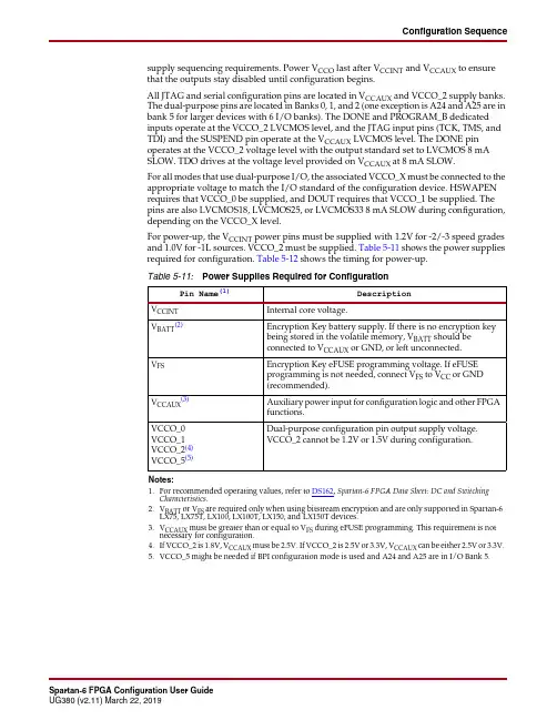
Configuration Sequence supply sequencing requirements. Power V CCO last after V CCINT and V CCAUX to ensurethat the outputs stay disabled until configuration begins.All JTAG and serial configuration pins are located in V CCAUX and VCCO_2 supply banks. The dual-purpose pins are located in Banks 0, 1, and 2 (one exception is A24 and A25 are in bank5 for larger devices with 6 I/O banks). The DONE and PROGRAM_B dedicated inputs operate at the VCCO_2 LVCMOS level, and the JTAG input pins (TCK, TMS, and TDI) and the SUSPEND pin operate at the V CCAUX LVCMOS level. The DONE pin operates at the VCCO_2 voltage level with the output standard set to LVCMOS 8mA SLOW. TDO drives at the voltage level provided on V CCAUX at 8 mA SLOW.For all modes that use dual-purpose I/O, the associated VCCO_X must be connected to the appropriate voltage to match the I/O standard of the configuration device. HSWAPEN requires that VCCO_0 be supplied, and DOUT requires that VCCO_1 be supplied. The pins are also LVCMOS18, LVCMOS25, or LVCMOS33 8mA SLOW during configuration, depending on the VCCO_X level.For power-up, the V CCINT power pins must be supplied with 1.2V for -2/-3 speed grades and 1.0V for -1L sources. VCCO_2 must be supplied. Table5-11 shows the power supplies required for configuration. Table5-12 shows the timing for power-up.Table 5-11:Power Supplies Required for ConfigurationPin Name(1)DescriptionV CCINT Internal core voltage.V BATT(2)Encryption Key battery supply. If there is no encryption keybeing stored in the volatile memory, V BATT should beconnected to V CCAUX or GND, or left unconnected.V FS Encryption Key eFUSE programming voltage. If eFUSEprogramming is not needed, connect V FS to V CC or GND(recommended).V CCAUX(3)Auxiliary power input for configuration logic and other FPGAfunctions.VCCO_0 VCCO_1 VCCO_2(4) VCCO_5(5)Dual-purpose configuration pin output supply voltage. VCCO_2 cannot be 1.2V or 1.5V during configuration.Notes:1.For recommended operating values, refer to DS162, Spartan-6 FPGA Data Sheet: DC and SwitchingCharacteristics.2.V BATT or V FS are required only when using bitstream encryption and are only supported in Spartan-6LX75, LX75T, LX100, LX100T, LX150, and LX150T devices.3.V CCAUX must be greater than or equal to V FS during eFUSE programming. This requirement is notnecessary for configuration.4.If VCCO_2 is 1.8V, V CCAUX must be 2.5V. If VCCO_2 is 2.5V or 3.3V, V CCAUX can be either 2.5V or 3.3V.5.VCCO_5 might be needed if BPI configuration mode is used and A24 and A25 are in I/O Bank 5.Chapter 5:Configuration DetailsConfiguration PacketsSuspend Register (PWRDN_REG)Frame Length RegisterFrame Length Register (FLR) is written with the length of a frame, as measured in 16-bit words, near the beginning of the configuration bitstream. FLR must be written before any FDR operation will work. It is not necessary to set the FLR more than once.The actual value written to FLR = Actual Frame Length.Based on the segmentation scheme in Spartan-6 devices, the frame length for type0 (CLB, IOI, and special blocks) and type1 (block RAM) are fixed. The only block that needs a specified frame length is IOB.Multi-Frame Write RegisterThe Spartan-6 FPGA supports Multi-Frame Write (MFWR) for first-time configuration but does not support it during reconfiguration. The FPGA has to go through one power cycle or use PROGRAM_B to reset the chip before MFWR can be used.Table 5-37:Power-Down Register Description Field Bit IndexDescriptionBitGen DefaultRESERVED 15Reserved.EN_EYES14Enable Multi-Pin Wake-Up.0: Disable Multi-Pin Wake-Up.1: Enable Multi-Pin Wake-Up.0RESERVED 13:6Reserved.0010_0010FILTER_B 50: Suspend filter (300ns) on.1: Filter off.0EN_PGSR40: No GSR pulse during return from Suspend.1: Generate GSR pulse during return from Suspend.0RESERVED 3Reserved.EN_PWRDN 20: Suspend is disabled.1: Suspend is enabled.0KEEP_SCLK0: Use MCCLK for startup sequence initiated by power-up.1: Use SSCLKSRC for startup sequence initiated by power-up.1Table 5-38:Frame Length RegisterBits FLR[15:0]xxxxxxxxxxxxxxxxChapter 5:Configuration DetailsConfiguration Watchdog Timer RegisterThe configuration watchdog timer (CWDT) register stores the value of the number of clock cycles that the FPGA will wait before the watchdog time-out (in which SYNCWORD is not received). The default is 64k clock cycles. The minimum value is 16h'0201.HC_OPT_REG RegisterThe HC_OPT_REG register can only be reset to default by por_b.GENERAL Registers 1, 2, 3, 4, and 5GENERAL1 and GENERAL2 registers are used to store loadable multiple configuration addresses for SPI and BPI.GENERAL3 and GENERAL4 registers have a similar function as GENERAL1 andGENERAL2, except that GENERAL3 and GENERAL4 store the golden bitstream address instead of the MultiBoot address.The GENERAL5 register is a 16-bit register that allows users to store and access any extra information desired for the fail-safe scheme. These register contents are untouched during a soft reboot.These registers are set by the bitstream. BitGen can be instructed not to write to these registers using the -g next_config_register_write:Disable command. This allows the ability to store user data in the FPGA between re-configuration attempts.If the second configuration needs a previously unknown SPI vendor command, the new vendor command has already been loaded in GENERAL2 from the bitstream by this point.Table 5-39:CWDT RegisterBits Value [15:0]16h'ffffTable 5-40:HC_OPT_REG DescriptionName Bits DescriptionDefault INIT_SKIP 60: Do not skip initialization.1: Skip initialization.0RESERVED5:0Reserved.011111Table 5-41:General RegistersName Bits DescriptionGENERAL1[15:0]The lower half of the multiple boot address.GENERAL2[15:0]15:8 – SPI opcode.7:0 – Higher half of the boot address.GENERAL3[15:0]The lower half of the golden bitstream address.GENERAL4[15:0]15:8 – SPI opcode.7:0 – Higher half of the golden boot address.GENERAL5[15:0]The user-defined scratchpad register.Configuration Packets。
FPGA可编程逻辑器件芯片XQ5VFX100T中文规格书
TDO_0
PROGRAM_B
CCLK_0
TCK_0
TMS
The RocketIO™ GTP transceiver I/O channels for the devices listed in Table 1-3 or the GTX transceiver I/O channels for the devices listed in Table 1-4.
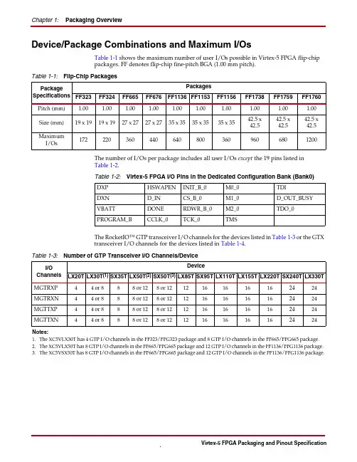
Table 1-1: Flip-Chip Packages
Package
Packages
Specifications FF323 FF324 FF665 FF676 FF1136 FF1153 FF1156
Pitch (mm) 1.00 1.00 1.00 1.00 1.00 1.00
1.00
Size (mm) 19 x 19 19 x 19 27 x 27 27 x 27 35 x 35 35 x 35 35 x 35
H13
24 IO_L7P_24
H10
24 IO_L7N_24
J10
24 IO_L8P_CC_24
H14
24 IO_L8N_CC_24(2 )
H15
24 IO_L9P_CC_24
K10
Virtex-5 FPGA Packaging and Pinout Specification
Maximum I/Os
172
220
360
440
640
800
360
FF1738 1.00 42.5 x 42.5
960
FF1759 1.00 42.5 x 42.5
680
FF1760 1.00 42.5 x 42.5
FPGA可编程逻辑器件芯片XC2V1000-5FFG896C中文规格书
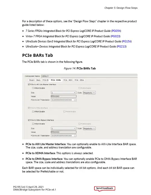
For a description of these options, see the “Design Flow Steps” chapter in the respective product guide listed below:•7 Series FPGAs Integrated Block for PCI Express LogiCORE IP Product Guide (PG054)•Virtex-7 FPGA Integrated Block for PCI Express LogiCORE IP Product Guide (PG023)•UltraScale Devices Gen3 Integrated Block for PCI Express LogiCORE IP Product Guide (PG156)•UltraScale+ Devices Integrated Block for PCI Express LogiCORE IP Product Guide (PG213)PCIe BARs TabThe PCIe BARs tab is shown in the following figure.Figure 14: PCIe BARs Tab•PCIe to AXI Lite Master Interface: You can optionally enable to AXI-Lite Interface BAR space.The size, scale, and address translation are configurable.•PCIe to XDMA Interface: This options is always selected.•PCIe to DMA Bypass Interface: You can optionally enable PCIe to DMA Bypass Interface BAR space. The size, scale and address translations are also configurable.Each BAR space can be individually selected for 64 bit options. And each 64 bit BAR space can be selected for Prefetchable or not.PCIe MISC TabThe PCIe Miscellaneous tab is shown in the following figure.Figure 15: PCIe Misc Tab•Number of User Interrupt Request: Up to 16 user interrupt requests can be selected.•Legacy Interrupt Settings: Select one of the Legacy Interrupts: INTA, INTB, INTC, or INTD.•MSI Capabilities: By default, MSI Capabilities is enabled, and 1 vector is enabled. You can choose up to 32 vectors. In general, Linux uses only 1 vector for MSI. This option can be disabled.•MSI RX PIN EN: This option is valid only in AXI Bridge Root Port mode.Chapter 5: Design Flow Steps •MSI-X Capabilities: Select a MSI-X event. For more information, see MSI-X Vector Table andPBA (0x8).•Finite Completion Credits: On systems which support finite completion credits, this option can be enabled for better performance.•Extended Tag Field: By default, 6-bit completion tags are used. For UltraScale™ and Virtex®-7 devices, the Extended Tag option gives 64 tags. For UltraScale+™ devices, the Extended Tag option gives 256 tags. If the Extended Tag option is not selected, DMA uses 32 tag for all devices.•Configuration Extend Interface: PCIe extended interface can be selected for more configuration space. When Configuration Extend Interface is selected, you are responsible for adding logic to extend the interface to make it work properly.•Configuration Management Interface: PCIe Configuration Management interface can be brought to the top level when this options is selected.•Link Status Register: By default, Enable Slot Clock Configuration is selected. This means that the slot configuration bit is enabled in the link status register.PCIe DMA TabThe PCIe DMA tab is shown in the following figure.PCIe DMA TabFigure 16:•Number of DMA Read Channels: Available selection is from 1 to 4.•Number of DMA Write Channels: Available selection is from 1 to 4.。
FPGA可编程逻辑器件芯片XC2V1000-5FF1704C中文规格书
Chapter 4: Designing with the SubsystemChapter 4Designing with the Subsystem This section includes guidelines and additional information to facilitate designing with thesubsystem.Clocking and ResetsClockingThe axi_aclk output is the clock used for all AXI interfaces and should drive all corresponding AXI Interconnect aclk signals. axi_aclk is not a free running clock. This is a derived clock and will be valid after signal axi_aresetn is de-assertedNote: The axi_aclk output should not be used for the system clock for your design. The axi_aclk isnot a free-run clock output. As noted, axi_aclk may not be present at all times.ResetsFor the DMA/ Bridge Subsystem for PCIe in AXI Bridge mode, there is an optionaldma_bridge_resetn input pin which allows you to reset all internal Bridge engines andregisters as well as all AXI peripherals driven by axi_aresetn pin. When the followingparameter is set, dma_bridge_resetn does not need to be asserted during initial link upoperation because it will be done automatically by the IP. You must terminate all transactionsbefore asserting this pin. After being asserted, the pin must be kept asserted for a minimumduration of at least equal to the Completion Timeout value (typically 50 ms) to clear any pending transfer that may currently be queued in the data path. T o set this parameter, type the following command at the T cl command line:set_property -dict [list CONFIG.soft_reset_en {true} [get_ips <ip_name>]For information about clocking and resets, see the applicable PCIe® integrated block productguide:•7 Series FPGAs Integrated Block for PCI Express LogiCORE IP Product Guide (PG054)•Virtex-7 FPGA Integrated Block for PCI Express LogiCORE IP Product Guide (PG023)•UltraScale Devices Gen3 Integrated Block for PCI Express LogiCORE IP Product Guide (PG156)PG195 (v4.1) April 29, 2021DMA/Bridge Subsystem for PCIe v4.1Send FeedbackChapter 4: Designing with the Subsystem •UltraScale+ Devices Integrated Block for PCI Express LogiCORE IP Product Guide (PG213)Tandem ConfigurationTandem Configuration features are available for the Xilinx® DMA Subsystem for PCI Express® for all UltraScale™ and most UltraScale+™ devices. Tandem Configuration uses a two-stagemethodology that enables the IP to meet the configuration time requirements indicated in thePCI Express Specification.Multiple use cases are supported with this technology:•Tandem PROM: Load the single two-stage bitstream from the flash.•Tandem PCIe: Load the first stage bitstream from flash, and deliver the second stage bitstream over the PCIe link to the MCAP.•Tandem with Field Updates: After a Tandem PROM (UltraScale only) or Tandem PCIe initial configuration, update the entire user design while the PCIe link remains active. The updateregion (floorplan) and design structure are predefined, and T cl scripts are provided.•Tandem + Dynamic Function eXchange: This is a more general case of Tandem Configuration followed by Dynamic Function eXchange (DFX) of any size or number of dynamic regions.•Dynamic Function eXchange over PCIe: This is a standard configuration followed by DFX, using the PCIe/MCAP as the delivery path of partial bitstreams.For information on Dynamic Function eXchange, see the Vivado Design Suite User Guide: Dynamic Function eXchange (UG909).Customizing the Subsystem for TandemConfigurationUltraScale DevicesT o enable any of the Tandem Configuration capabilities for UltraScale™ devices, select theappropriate Vivado® IP catalog option when customizing the subsystem. In the Basic tab:1.Change the Mode to Advanced.2.Change the Tandem Configuration or Dynamic Function eXchange option according to yourparticular case:•Tandem: For Tandem PROM, Tandem PCIe or Tandem + Dynamic Function eXchange use cases.•Tandem with Field Updates: ONLY for the predefined Field Updates use case.•DFX over PCIe: T o enable the MCAP link for Dynamic Function eXchange, without enabling Tandem Configuration.PG195 (v4.1) April 29, 2021DMA/Bridge Subsystem for PCIe v4.1Send FeedbackFigure 10: Tandem Configuration or Dynamic Function eXchangeOptions forUltraScale DevicesFor complete information about Tandem Configuration, including required PCIe block locations,design flow examples, requirements, restrictions and other considerations, see TandemConfiguration in the UltraScale Devices Gen3 Integrated Block for PCI Express LogiCORE IP Product Guide (PG156).UltraScale+ DevicesT o enable any of the Tandem Configuration capabilities for UltraScale+™ devices, select the appropriate IP catalog option when customizing the subsystem. In the Basic tab:1.Change the Mode to Advanced .2.Change the Tandem Configuration or Dynamic Function eXchange option according to yourparticular case:•Tandem PROM: For the Tandem PROM use case.•Tandem PCIe: For Tandem PCIe or Tandem + Dynamic Function eXchange use cases.•Tandem PCIe with Field Updates: ONLY for the predefined Field Updates use case.•DFX over PCIe: T o enable the MCAP link for Dynamic Function eXchange, without enabling Tandem Configuration.Figure 11:Tandem Configuration or Dynamic Function eXchange OptionIMPORTANT! Tandem Configuration is currently supported for DMA mode, and is not supported for Bridge mode in UltraScale+ devices.Chapter 4: Designing with the SubsystemPG195 (v4.1) April 29, 2021DMA/Bridge Subsystem for PCIe v4.1Send Feedback。
FPGA可编程逻辑器件芯片EP1C6T144I7N中文规格书
SPI-Compatible Port Controllers3.The core writes to the SPIx_BAUD and SPIx_CTL registers, enablingthe device as a master and configuring the SPI system by specifyingthe appropriate word length, transfer format, baud rate, and othernecessary information.4.If CPHA = 1, the core activates the desired slaves by clearing one ormore of the SPI flag bits (FLGx) of SPIx_FLG.5.The TIMOD bits in SPIx_CTL determine the SPI transfer initiatemode. The transfer on the SPI link begins upon either a data writeby the core to the transmit data buffer(SPIx_TDBR) or a data readof the receive data buffer (SPIx_RDBR).6.The SPI then generates the programmed clock pulses on SPIxSCKand simultaneously shifts data out of SPIx MOSI and shifts data infrom SPIxMISO. Before a shift, the shift register is loaded with thecontents of the SPIx_TDBR register. At the end of the transfer, thecontents of the shift register are loaded into SPIx_RDBR.7.With each new transfer initiate command, the SPI continues tosend and receive words, according to the SPI transfer initiate mode.See Figure22-8 on page22-39 for additional information.If the transmit buffer remains empty or the receive buffer remains full, thedevice operates according to the states of the SZ and GM bits in SPIx_CTL. If SZ = 1 and the transmit buffer is empty, the device repeatedly transmits 0s on the SPIxMOSI pin. One word is transmitted for each new transfer initi-ate command. If SZ = 0 and the transmit buffer is empty, the devicerepeatedly transmits the last word it transmitted before the transmit buffer became empty. If GM = 1 and the receive buffer is full, the device continues to receive new data from the SPIxMISO pin, overwriting the older data in the SPIx_RDBR buffer. If GM = 0 and the receive buffer is full, the incoming data is discarded, and SPIx_RDBR is not updated.ADSP-BF54x Blackfin Processor Hardware ReferenceSPI-Compatible Port ControllersFigure 22-7. SPI Transfer Protocol for CPHA=1SPI General OperationEach SPI can be used in a single master as well as multimaster environ-ment. The SPIxMOSI, SPIxMISO, and the SPIxSCK signals are all tiedtogether in both configurations. SPI transmission and reception are always enabled simultaneously, unless the broadcast mode is selected. In broad-cast mode, several slaves can be enabled to receive, but only one of the slaves must be in transmit mode driving the SPIxMISO line. If the transmit or receive is not needed, it can simply be ignored. This section describes the clock signals, SPI operation as a master and as a slave, and errorgeneration.Precautions must be taken to avoid data corruption when changing the SPI module configuration. The configuration must not be changed duringa data transfer. The clock polarity should only be changed when no slavesare selected. An exception to this is when an SPI communication link con-sists of a single master and a single slave, CPHA = 1, and the slave select input of the slave is always tied low. In this case, the slave is alwaysselected and data corruption can be avoided by enabling the slave only after both the master and slave devices are configured.ADSP-BF54x Blackfin Processor Hardware Reference。
FPGA可编程逻辑器件芯片EPM240T100C5N中文规格书
Stratix II GX Architecture Drivers from internal logic GCLKDRV0v v GCLKDRV1v v GCLKDRV2v v GCLKDRV3v v RCLKDRV0v v RCLKDRV1v vRCLKDRV2v vRCLKDRV3vv RCLKDRV4vv RCLKDRV5vv RCLKDRV6vv RCLKDRV7vv PLL 1 outputs c0vv v v v v c1v vv v v v c2vv v v v v c3vv v v v v PLL 2 outputs c0vv v v v v c1v vv v v v c2vv v v v v c3vv v v v v PLL 7 outputs c0vv v v c1vv v v c2vv v v c3v v v v Table 2–27.Global and Regional Clock Connections from Left Side Clock Pins and Fast PLL Outputs (Part 2 of 3)Left Side Global and Regional Clock Network Connectivity C L K 0C L K 1C L K 2C L K 3R C L K 0R C L K 1R C L K 2R C L K 3R C L K 4R C L K 5R C L K 6R C L K 7TriMatrix MemoryTriMatrix memory provides three different memory sizes for efficientapplication support. The Quartus II software automatically partitions theuser-defined memory into the embedded memory blocks using the mostefficient size combinations. You can also manually assign the memory toa specific block size or a mixture of block sizes.M512 RAM BlockThe M512 RAM block is a simple dual-port memory block and is usefulfor implementing small FIFO buffers, DSP , and clock domain transferapplications. Each block contains 576 RAM bits (including parity bits).M512 RAM blocks can be configured in the following modes:■Simple dual-port RAM ■Single-port RAM ■FIFO ■ROM ■Shift registerWhen configured as RAM or ROM, you can use an initialization file topre-load the memory contents.Simple dual-port memorymixed width supportv v v T rue dual-port memorymixed width supportv v Power-up conditionsOutputs cleared Outputs cleared Outputs unknown Register clearsOutput registers Output registers Output registers Mixed-port read-during-writeUnknown output/old data Unknown output/old dataUnknown output Configurations 512 × 1256 × 2128 × 464 × 864 × 932 × 1632 × 184K × 12K × 21K × 4512 × 8512 × 9256 × 16256 × 18128 × 32128 × 3664K × 864K × 932K × 1632K × 1816K × 3216K × 368K × 648K × 724K × 1284K × 144Note to Table 2–19:(1)Violating the setup or hold time on the memory block address registers could corrupt memory contents. Thisapplies to both read and write operations.Table 2–19.TriMatrix Memory Features (Part 2 of 2)Memory FeatureM512 RAM Block (32×18 Bits)M4K RAM Block (128×36 Bits)M-RAM Block (4K ×144Bits)Digital Signal Processing (DSP) BlockFigure2–58.DSP Block Diagram for 18 × 18-Bit Configuration。
FPGA可编程逻辑器件芯片EPF10K10TI144-4中文规格书
Referenced DocumentsFigure2–91.Fast PLL and Channel Layout in the EP2SGX60E to EP2SGX130 Devices Note(1) Note to Figure2–91:(1)See Tables2–39 through Tables2–41 for the number of channels each device supports.Referenced Documents This chapter references the following documents:■DC & Switching Characteristics chapter in volume 1 of the Stratix II GX Handbook■DSP Blocks in Stratix II GX Devices chapter in Volume 2 of the Stratix II GX Device Handbook■External Memory Interfaces in Stratix II & Stratix II GX Devices chapter in volume 2 of the Stratix II GX Device Handbook■High-Speed Differential I/O Interfaces with DP A in Stratix II & Stratix II GX Devices chapter in volume 2 of the Stratix II GX Handbook■PLLs in Stratix II & Stratix II GX Devices chapter in volume 2 of the Stratix II GX Device Handbook■Selectable I/O Standards in Stratix II & Stratix II GX Devices chapter in volume 2 of the Stratix II GX Handbook■Stratix II GX Device Handbook, volume 2■Stratix II GX Transceiver Architecture Overview chapter in volume 2 of the Stratix II GX HandbookOperating ConditionsFigure4–4.Transmitter Output WaveformFigure4–5.Maximum Receiver Input Pin VoltageNote to Figure4–5:(1)The absolute V MAX that the receiver input pins can tolerate is 2V.Tables4–7 through 4–12 show the typical V OD for data rates from600Mbps to 6.375Gbps. The specification is for measurement at thepackage ball.Table4–7.Typical V OD Setting, TX Term = 100 ΩNote(1)V C C H TX = 1.5V V OD Setting (mV)200400600800100012001400 V OD Typical (mV)220430625830102012001350 Note to Table4–7:(1)Applicable to data rates from 600 Mbps to 6.375Gbps. Specification is for measurement at the package ball.Configuration & TestingTable 3–5 shows the specifications for bias voltage and current of the Stratix II GX temperature sensing diode.The temperature-sensing diode works for the entire operating range shown in Figure 3–2.Figure 3–2.Temperature Versus Temperature-Sensing Diode Voltage Table 3–5.Temperature-Sensing Diode Electrical Characteristics ParameterMinimum Typical Maximum Unit IBIAS high80100120 μA IBIAS low81012 μA VBP - VBN0.30.9V VBN0.7V Series resistance 3Ω。
FPGA可编程逻辑器件芯片XC2S200EFT256中文规格书
Design ConsiderationsThe Basic Configuration SolutionA basic option is Master Serial mode using a third-party SPI flash. This solution uses thefewest FPGA pins, has flexible I/O voltage support, and select SPI flash memories aresupported by iMPACT, the Xilinx JTAG-based programming software.The Low-Cost Priority SolutionThe option with the lowest cost varies depending on the specific application.•If there is spare nonvolatile memory already available in the system, the bitstream image can be stored in system memory. It can even be stored on a hard drive ordownloaded remotely over a network connection. If so, one of the downloadedmodes should be considered:Slave SelectMAP Mode, Slave Serial Mode, or JTAG.•If nonvolatile memory is already required for an application, it is possible toconsolidate the memory. For example, the FPGA configuration bitstream(s) can bestored with any processor code for the board. If the processor is a MicroBlaze™embedded processor in the FPGA, the FPGA configuration data and the MicroBlazeprocessor code can share the same nonvolatile memory device.•Spartan-6 FPGAs can configure directly from commodity SPI serial flash and parallel NOR flash memories. See Chapter2, Configuration Interface Basics. Also seeXAPP973, Indirect Programming of BPI PROMs with Virtex-5 FPGAs, and XAPP974,Indirect Programming of SPI Serial Flash PROMs with Spartan-3A FPGAs.The High-Speed Priority OptionSome applications require the logic to be operational within a short time. Certain FPGAconfiguration modes and methods are faster than others. The configuration time includesthe initialization time plus the configuration time. Configuration time depends on the sizeof the device and speed of the configuration logic. For example, configuring at 33MHzwith a 4-bit data bus, a Spartan-6 XC6SLX16 FPGA requires ~28ms to receive its 3.6Mb ofconfiguration data.•At the same clock frequency, parallel configuration modes are inherently faster than the serial modes because they program multiple bits at a time.•Configuring a single FPGA is inherently faster than configuring multiple FPGAs in a daisy-chain. In a multi-FPGA design where configuration speed is a concern, eachFPGA should be configured separately and in parallel.•In Master modes, the FPGA internally generates the CCLK configuration clock signal.By default, the CCLK frequency starts out low but can be increased using theConfigRate bitstream option. The maximum supported CCLK frequency settingdepends on the read specifications for the attached nonvolatile memory. A fastermemory enables faster configuration. The FPGA's CCLK output frequency varieswith process, voltage, and temperature. The fastest guaranteed configuration ratedepends on the slowest guaranteed CCLK frequency, as shown in the Spartan-6FPGAdata sheet. If an external clock is available on the board, it is also possible to configurethe FPGA in Slave mode while using Xilinx Platform Flash.•If an external clock is available on the board, the FPGA supports the ability to connect and use an external clock source during Master mode configuration. It is also possibleto use an external clock source to configure the FPGA in a slave mode while usingXilinx Platform Flash. The external clock source during configuration enablespredictable configuration times to be achieved in Master modes as well as Slavemodes.Chapter 2:Configuration Interface BasicsMaster SerialThe Master Serial configuration is designed so that the FPGA can be configured from aXilinx® Platform Flash PROM, as shown in Figure2-2.Figure 2-2:Master Serial Mode ConfigurationNotes relevant to Figure2-2:1.See Table5-2, page74 for internal pin terminations and pins affected by HSWAPEN.2.DOUT should be connected to the DIN of the downstream FPGA for daisy-chainedconfiguration modes.3.The CCLK net requires Thevenin parallel termination. For details, refer to BoardLayout for Configuration Clock (CCLK), page56.4.Master Serial and Master SPI are both enabled from the same mode pins. Therefore, theSPI control pins, CSO_B and MOSI, toggle during configuration.SelectMAP Configuration Interface3.For more details on CCLK termination, see Board Layout for Configuration Clock(CCLK), page56.4.This schematic is from XAPP502, Using a Microprocessor to Configure Xilinx FPGAs viaSlave Serial or SelectMAP Mode. It is one of many possible implementations.5.The DONE pin is by default an open-drain output with an internal pull-up. Anadditional external pull-up is recommended. The DONE pin has a programmableactive driver that can be enabled via the BitGen option -g DriveDone.6.The INIT_B pin is a bidirectional, open-drain pin. An external pull-up resistor isrecommended.7.The BitGen startup clock setting must be set for CCLK for SelectMAP configuration.8.The CSI_B and RDWR_B signals can be tied to ground if only one FPGA is going to beconfigured and readback is not needed.9.The D[0:n] bus can be x8 or x16 for Slave SelectMAP configuration.10.V FS is present in 6SLX75/T, 6SLX100/T, and 6SLX150/T devices, and is used foreFUSE programming. See eFUSE, page93 for more details.11.V BATT is present in 6SLX75/T, 6SLX100/T, and 6SLX150/T devices, and is the powersource for AES key storage. If AES encryption is unused, V BATT can be tied to eitherV CCAUX or ground, or left unconnected.12.If VCCO_2 is 1.8V, V CCAUX must be 2.5V. If VCCO_2 is 2.5V or 3.3V, V CCAUX can beeither 2.5V or 3.3V.13.The SUSPEND pin should be Low during power up and configuration. If the Suspendfeature is not used, the SUSPEND pin must be connected to ground.SelectMAP Data LoadingThe SelectMAP interface allows for either continuous or non-continuous data loading.Data loading is controlled by the CSI_B, RDWR_B, and CCLK signals.CSI_BThe Chip Select input (CSI_B) enables the SelectMAP bus. CSI_B should not be deassertedin the middle of a sync word. When CSI_B is High, the Spartan-6 device ignores theSelectMAP interface, neither registering any inputs nor driving any outputs. D[0:n] isplaced in a High-Z state, and RDWR_B is ignored.•If CSI_B=0, the device's SelectMAP interface is enabled.•If CSI_B=1, the device's SelectMAP interface is disabled.For a multiple device SelectMAP configuration, refer to Chapter9, AdvancedConfiguration Interfaces.If only one device is being configured through the SelectMAP interface and readback is notrequired, or if ganged SelectMAP configuration is used, the CSI_B signal can be tied toground, as illustrated in Chapter9, Advanced Configuration Interfaces.Chapter 2:Configuration Interface BasicsChapter 3:Boundary-Scan and JTAG Configuration。
- 1、下载文档前请自行甄别文档内容的完整性,平台不提供额外的编辑、内容补充、找答案等附加服务。
- 2、"仅部分预览"的文档,不可在线预览部分如存在完整性等问题,可反馈申请退款(可完整预览的文档不适用该条件!)。
- 3、如文档侵犯您的权益,请联系客服反馈,我们会尽快为您处理(人工客服工作时间:9:00-18:30)。
This document includes all four modules of the Spartan ®-II FPGA data sheet.Module 1:Introduction and Ordering InformationDS001-1 (v2.8) June 13, 2008•Introduction •Features•General Overview •Product Availability •User I/O Chart•Ordering InformationModule 2:Functional DescriptionDS001-2 (v2.8) June 13, 2008•Architectural Description -Spartan-II Array -Input/Output Block-Configurable Logic Block -Block RAM-Clock Distribution: Delay-Locked Loop -Boundary Scan •Development System •Configuration-Configuration Timing •Design ConsiderationsModule 3:DC and Switching CharacteristicsDS001-3 (v2.8) June 13, 2008•DC Specifications-Absolute Maximum Ratings-Recommended Operating Conditions -DC Characteristics-Power-On Requirements -DC Input and Output Levels •Switching Characteristics -Pin-to-Pin Parameters-IOB Switching Characteristics -Clock Distribution Characteristics -DLL Timing Parameters-CLB Switching Characteristics-Block RAM Switching Characteristics -TBUF Switching Characteristics -JT AG Switching CharacteristicsModule 4: Pinout TablesDS001-4 (v2.8) June 13, 2008•Pin Definitions •Pinout TablesIMPORTANT NOTE: This Spartan-II FPGA data sheet is in four modules. Each module has its own Revision History at the end. Use the PDF "Bookmarks" for easy navigation in this volume.DS001 June 13, 2008Product Specification找FPGA ,上赛灵思半导体(深圳)有限公司DS001-1 (v2.8) June 13, 2008Product SpecificationDeviceLogic Cells System Gates (Logic and RAM)CLB Array (R x C)Total CLBs Maximum Available User I/O (1)TotalDistributed RAMBitsTotal Block RAMBitsXC2S1543215,0008 x 1296866,14416K XC2S3097230,00012 x 182169213,82424K XC2S501,72850,00016 x 2438417624,57632K XC2S1002,700100,00020 x 3060017638,40040K XC2S1503,888150,00024 x 3686426055,29648K XC2S2005,292200,00028 x 421,17628475,26456KSpartan-II FPGA Family: Introduction and Ordering InformationGeneral OverviewThe Spartan-II family of FPGAs have a regular, flexible, programmable architecture of Configurable Logic Blocks (CLBs), surrounded by a perimeter of programmable Input/Output Blocks (IOBs). There are four Delay-Locked Loops (DLLs), one at each corner of the die. Two columns of block RAM lie on opposite sides of the die, between the CLBs and the IOB columns. These functional elements are interconnected by a powerful hierarchy of versatile routing channels (see Figure1).Spartan-II FPGAs are customized by loading configuration data into internal static memory cells. Unlimited reprogramming cycles are possible with this approach. Stored values in these cells determine logic functions and interconnections implemented in the FPGA. Configuration data can be read from an external serial PROM (master serial mode), or written into the FPGA in slave serial, slave parallel, or Boundary Scan modes.Spartan-II FPGAs are typically used in high-volume applications where the versatility of a fast programmable solution adds benefits. Spartan-II FPGAs are ideal for shortening product development cycles while offering a cost-effective solution for high volume production. Spartan-II FPGAs achieve high-performance, low-cost operation through advanced architecture and semiconductor technology. Spartan-II devices provide system clock rates up to 200MHz. In addition to the conventional benefits of high-volume programmable logic solutions, Spartan-II FPGAs also offer on-chip synchronous single-port and dual-port RAM (block and distributed form), DLL clock drivers, programmable set and reset on allflip-flops, fast carry logic, and many other features.Similarly, the F6 multiplexer combines the outputs of all four function generators in the CLB by selecting one of theF5-multiplexer outputs. This permits the implementation of any 6-input function, an 8:1 multiplexer, or selected functions of up to 19 inputs.Each CLB has four direct feedthrough paths, one per LC. These paths provide extra data input lines or additional local routing that does not consume logic resources.Arithmetic LogicDedicated carry logic provides capability for high-speed arithmetic functions. The Spartan-II FPGA CLB supports two separate carry chains, one per slice. The height of the carry chains is two bits per CLB.The arithmetic logic includes an XOR gate that allows a1-bit full adder to be implemented within an LC. In addition, a dedicated AND gate improves the efficiency of multiplier implementation.The dedicated carry path can also be used to cascade function generators for implementing wide logic functions. BUFTsEach Spartan-II FPGA CLB contains two 3-state drivers (BUFTs) that can drive on-chip busses. See "Dedicated Routing," page12. Each Spartan-II FPGA BUFT has an independent 3-state control pin and an independent input pin.Block RAMSpartan-II FPGAs incorporate several large block RAM memories. These complement the distributed RAMLook-Up Tables (LUTs) that provide shallow memory structures implemented in CLBs.Block RAM memory blocks are organized in columns. All Spartan-II devices contain two such columns, one along each vertical edge. These columns extend the full height of the chip. Each memory block is four CLBs high, and consequently, a Spartan-II device eight CLBs high will contain two memory blocks per column, and a total of four blocks. Each block RAM cell, as illustrated in Figure5, is a fully synchronous dual-ported 4096-bit RAM with independent control signals for each port. The data widths of the two ports can be configured independently, providing built-in bus-width conversion.Table6 shows the depth and width aspect ratios for the block RAM.The Spartan-II FPGA block RAM also includes dedicated routing to provide an efficient interface with both CLBs and other block RAMs.Programmable Routing MatrixIt is the longest delay path that limits the speed of any worst-case design. Consequently, the Spartan-II routing architecture and its place-and-route software were defined in a single optimization process. This joint optimization minimizes long-path delays, and consequently, yields the best system performance.The joint optimization also reduces design compilation times because the architecture is software-friendly. Design cycles are correspondingly reduced due to shorter design iteration times.Table 5: Spartan-II Block RAM AmountsSpartan-IIDevice# of Blocks Total Block RAMBitsXC2S15416K XC2S30624K XC2S50832K XC2S1001040K XC2S1501248K XC2S2001456KFigure 5: Dual-Port Block RAMTable 6: Block RAM Port Aspect RatiosWidth Depth ADDR Bus Data Bus 14096ADDR<11:0>DA TA<0>22048ADDR<10:0>DA TA<1:0>41024ADDR<9:0>DA TA<3:0>8512ADDR<8:0>DA TA<7:0> 16256ADDR<7:0>DATA<15:0>Local RoutingThe local routing resources, as shown in Figure6, provide the following three types of connections:•Interconnections among the LUTs, flip-flops, and General Routing Matrix (GRM)•Internal CLB feedback paths that provide high-speed connections to LUTs within the same CLB, chaining them together with minimal routing delay•Direct paths that provide high-speed connections between horizontally adjacent CLBs, eliminating the delay of the GRMefficiently. Vertical Longlines span the full height of the device, and horizontal ones span the full width of thedevice.I/O RoutingSpartan-II devices have additional routing resources around their periphery that form an interface between the CLB array and the IOBs. This additional routing, called the VersaRing, facilitates pin-swapping and pin-locking, such that logic redesigns can adapt to existing PCB layouts. Time-to-market is reduced, since PCBs and other system components can be manufactured while the logic design is still in progress.Dedicated RoutingSome classes of signal require dedicated routing resources to maximize performance. In the Spartan-II architecture, dedicated routing resources are provided for two classes of signal.•Horizontal routing resources are provided for on-chip 3-state busses. Four partitionable bus lines areprovided per CLB row, permitting multiple busseswithin a row, as shown in Figure7.•Two dedicated nets per CLB propagate carry signals vertically to the adjacent CLB.。