Lattice Models of Random Geometries
阿贡实验室RietveldRefinementwithGSAS

5
Errors & parameters?
position – lattice parameters, zero point (not common)
- other systematic effects – sample shift/offset shape – profile coefficients (GU, GV, GW, LX, LY, etc. in GSAS) intensity – crystal structure (atom positions & thermal parameters)
9
So how does Rietveld refinement work?
Rietveld Minimize
MR w(Io Ic )2
Io
Exact overlaps - symmetry
Incomplete overlaps
SIc
Residuals:
Rwp
w(I o Ic )2
wI
c2
Least-squares cycles
False minimum
True minimum – “global” minimum
parameter c2 surface shape depends on parameter suite
3
Fluoroapatite start – add model (1st choose lattice/sp. grp.)
c
5i
ig
i
i1
18
Collective dynamics of 'small-world' networks
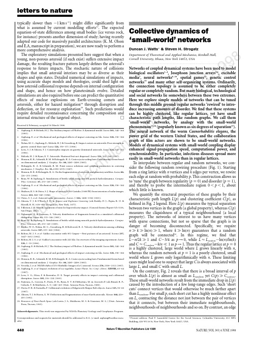
Nature © Macmillan Publishers Ltd 19988typically slower than ϳ1km s −1)might differ significantly from what is assumed by current modelling efforts 27.The expected equation-of-state differences among small bodies (ice versus rock,for instance)presents another dimension of study;having recently adapted our code for massively parallel architectures (K.M.Olson and E.A,manuscript in preparation),we are now ready to perform a more comprehensive analysis.The exploratory simulations presented here suggest that when a young,non-porous asteroid (if such exist)suffers extensive impact damage,the resulting fracture pattern largely defines the asteroid’s response to future impacts.The stochastic nature of collisions implies that small asteroid interiors may be as diverse as their shapes and spin states.Detailed numerical simulations of impacts,using accurate shape models and rheologies,could shed light on how asteroid collisional response depends on internal configuration and shape,and hence on how planetesimals evolve.Detailed simulations are also required before one can predict the quantitative effects of nuclear explosions on Earth-crossing comets and asteroids,either for hazard mitigation 28through disruption and deflection,or for resource exploitation 29.Such predictions would require detailed reconnaissance concerning the composition andinternal structure of the targeted object.ⅪReceived 4February;accepted 18March 1998.1.Asphaug,E.&Melosh,H.J.The Stickney impact of Phobos:A dynamical model.Icarus 101,144–164(1993).2.Asphaug,E.et al .Mechanical and geological effects of impact cratering on Ida.Icarus 120,158–184(1996).3.Nolan,M.C.,Asphaug,E.,Melosh,H.J.&Greenberg,R.Impact craters on asteroids:Does strength orgravity control their size?Icarus 124,359–371(1996).4.Love,S.J.&Ahrens,T.J.Catastrophic impacts on gravity dominated asteroids.Icarus 124,141–155(1996).5.Melosh,H.J.&Ryan,E.V.Asteroids:Shattered but not dispersed.Icarus 129,562–564(1997).6.Housen,K.R.,Schmidt,R.M.&Holsapple,K.A.Crater ejecta scaling laws:Fundamental forms basedon dimensional analysis.J.Geophys.Res.88,2485–2499(1983).7.Holsapple,K.A.&Schmidt,R.M.Point source solutions and coupling parameters in crateringmechanics.J.Geophys.Res.92,6350–6376(1987).8.Housen,K.R.&Holsapple,K.A.On the fragmentation of asteroids and planetary satellites.Icarus 84,226–253(1990).9.Benz,W.&Asphaug,E.Simulations of brittle solids using smooth particle put.mun.87,253–265(1995).10.Asphaug,E.et al .Mechanical and geological effects of impact cratering on Ida.Icarus 120,158–184(1996).11.Hudson,R.S.&Ostro,S.J.Shape of asteroid 4769Castalia (1989PB)from inversion of radar images.Science 263,940–943(1994).12.Ostro,S.J.et al .Asteroid radar astrometry.Astron.J.102,1490–1502(1991).13.Ahrens,T.J.&O’Keefe,J.D.in Impact and Explosion Cratering (eds Roddy,D.J.,Pepin,R.O.&Merrill,R.B.)639–656(Pergamon,New York,1977).14.Tillotson,J.H.Metallic equations of state for hypervelocity impact.(General Atomic Report GA-3216,San Diego,1962).15.Nakamura,A.&Fujiwara,A.Velocity distribution of fragments formed in a simulated collisionaldisruption.Icarus 92,132–146(1991).16.Benz,W.&Asphaug,E.Simulations of brittle solids using smooth particle put.mun.87,253–265(1995).17.Bottke,W.F.,Nolan,M.C.,Greenberg,R.&Kolvoord,R.A.Velocity distributions among collidingasteroids.Icarus 107,255–268(1994).18.Belton,M.J.S.et al .Galileo encounter with 951Gaspra—First pictures of an asteroid.Science 257,1647–1652(1992).19.Belton,M.J.S.et al .Galileo’s encounter with 243Ida:An overview of the imaging experiment.Icarus120,1–19(1996).20.Asphaug,E.&Melosh,H.J.The Stickney impact of Phobos:A dynamical model.Icarus 101,144–164(1993).21.Asphaug,E.et al .Mechanical and geological effects of impact cratering on Ida.Icarus 120,158–184(1996).22.Housen,K.R.,Schmidt,R.M.&Holsapple,K.A.Crater ejecta scaling laws:Fundamental forms basedon dimensional analysis.J.Geophys.Res.88,2485–2499(1983).23.Veverka,J.et al .NEAR’s flyby of 253Mathilde:Images of a C asteroid.Science 278,2109–2112(1997).24.Asphaug,E.et al .Impact evolution of icy regoliths.Lunar Planet.Sci.Conf.(Abstr.)XXVIII,63–64(1997).25.Love,S.G.,Ho¨rz,F.&Brownlee,D.E.Target porosity effects in impact cratering and collisional disruption.Icarus 105,216–224(1993).26.Fujiwara,A.,Cerroni,P .,Davis,D.R.,Ryan,E.V.&DiMartino,M.in Asteroids II (eds Binzel,R.P .,Gehrels,T.&Matthews,A.S.)240–265(Univ.Arizona Press,Tucson,1989).27.Davis,D.R.&Farinella,P.Collisional evolution of Edgeworth-Kuiper Belt objects.Icarus 125,50–60(1997).28.Ahrens,T.J.&Harris,A.W.Deflection and fragmentation of near-Earth asteroids.Nature 360,429–433(1992).29.Resources of Near-Earth Space (eds Lewis,J.S.,Matthews,M.S.&Guerrieri,M.L.)(Univ.ArizonaPress,Tucson,1993).Acknowledgements.This work was supported by NASA’s Planetary Geology and Geophysics Program.Correspondence and requests for materials should be addressed to E.A.(e-mail:asphaug@).letters to nature440NATURE |VOL 393|4JUNE 1998Collective dynamics of ‘small-world’networksDuncan J.Watts *&Steven H.StrogatzDepartment of Theoretical and Applied Mechanics,Kimball Hall,Cornell University,Ithaca,New York 14853,USA.........................................................................................................................Networks of coupled dynamical systems have been used to model biological oscillators 1–4,Josephson junction arrays 5,6,excitable media 7,neural networks 8–10,spatial games 11,genetic control networks 12and many other self-organizing systems.Ordinarily,the connection topology is assumed to be either completely regular or completely random.But many biological,technological and social networks lie somewhere between these two extremes.Here we explore simple models of networks that can be tuned through this middle ground:regular networks ‘rewired’to intro-duce increasing amounts of disorder.We find that these systems can be highly clustered,like regular lattices,yet have small characteristic path lengths,like random graphs.We call them ‘small-world’networks,by analogy with the small-world phenomenon 13,14(popularly known as six degrees of separation 15).The neural network of the worm Caenorhabditis elegans ,the power grid of the western United States,and the collaboration graph of film actors are shown to be small-world networks.Models of dynamical systems with small-world coupling display enhanced signal-propagation speed,computational power,and synchronizability.In particular,infectious diseases spread more easily in small-world networks than in regular lattices.To interpolate between regular and random networks,we con-sider the following random rewiring procedure (Fig.1).Starting from a ring lattice with n vertices and k edges per vertex,we rewire each edge at random with probability p .This construction allows us to ‘tune’the graph between regularity (p ¼0)and disorder (p ¼1),and thereby to probe the intermediate region 0Ͻp Ͻ1,about which little is known.We quantify the structural properties of these graphs by their characteristic path length L (p )and clustering coefficient C (p ),as defined in Fig.2legend.Here L (p )measures the typical separation between two vertices in the graph (a global property),whereas C (p )measures the cliquishness of a typical neighbourhood (a local property).The networks of interest to us have many vertices with sparse connections,but not so sparse that the graph is in danger of becoming disconnected.Specifically,we require n q k q ln ðn Þq 1,where k q ln ðn Þguarantees that a random graph will be connected 16.In this regime,we find that L ϳn =2k q 1and C ϳ3=4as p →0,while L ϷL random ϳln ðn Þ=ln ðk Þand C ϷC random ϳk =n p 1as p →1.Thus the regular lattice at p ¼0is a highly clustered,large world where L grows linearly with n ,whereas the random network at p ¼1is a poorly clustered,small world where L grows only logarithmically with n .These limiting cases might lead one to suspect that large C is always associated with large L ,and small C with small L .On the contrary,Fig.2reveals that there is a broad interval of p over which L (p )is almost as small as L random yet C ðp Þq C random .These small-world networks result from the immediate drop in L (p )caused by the introduction of a few long-range edges.Such ‘short cuts’connect vertices that would otherwise be much farther apart than L random .For small p ,each short cut has a highly nonlinear effect on L ,contracting the distance not just between the pair of vertices that it connects,but between their immediate neighbourhoods,neighbourhoods of neighbourhoods and so on.By contrast,an edge*Present address:Paul zarsfeld Center for the Social Sciences,Columbia University,812SIPA Building,420W118St,New York,New York 10027,USA.Nature © Macmillan Publishers Ltd 19988letters to natureNATURE |VOL 393|4JUNE 1998441removed from a clustered neighbourhood to make a short cut has,at most,a linear effect on C ;hence C (p )remains practically unchanged for small p even though L (p )drops rapidly.The important implica-tion here is that at the local level (as reflected by C (p )),the transition to a small world is almost undetectable.To check the robustness of these results,we have tested many different types of initial regular graphs,as well as different algorithms for random rewiring,and all give qualitatively similar results.The only requirement is that the rewired edges must typically connect vertices that would otherwise be much farther apart than L random .The idealized construction above reveals the key role of short cuts.It suggests that the small-world phenomenon might be common in sparse networks with many vertices,as even a tiny fraction of short cuts would suffice.To test this idea,we have computed L and C for the collaboration graph of actors in feature films (generated from data available at ),the electrical power grid of the western United States,and the neural network of the nematode worm C.elegans 17.All three graphs are of scientific interest.The graph of film actors is a surrogate for a social network 18,with the advantage of being much more easily specified.It is also akin to the graph of mathematical collaborations centred,traditionally,on P.Erdo¨s (partial data available at /ϳgrossman/erdoshp.html).The graph of the power grid is relevant to the efficiency and robustness of power networks 19.And C.elegans is the sole example of a completely mapped neural network.Table 1shows that all three graphs are small-world networks.These examples were not hand-picked;they were chosen because of their inherent interest and because complete wiring diagrams were available.Thus the small-world phenomenon is not merely a curiosity of social networks 13,14nor an artefact of an idealizedmodel—it is probably generic for many large,sparse networks found in nature.We now investigate the functional significance of small-world connectivity for dynamical systems.Our test case is a deliberately simplified model for the spread of an infectious disease.The population structure is modelled by the family of graphs described in Fig.1.At time t ¼0,a single infective individual is introduced into an otherwise healthy population.Infective individuals are removed permanently (by immunity or death)after a period of sickness that lasts one unit of dimensionless time.During this time,each infective individual can infect each of its healthy neighbours with probability r .On subsequent time steps,the disease spreads along the edges of the graph until it either infects the entire population,or it dies out,having infected some fraction of the population in theprocess.p = 0p = 1Regular Small-worldRandomFigure 1Random rewiring procedure for interpolating between a regular ring lattice and a random network,without altering the number of vertices or edges in the graph.We start with a ring of n vertices,each connected to its k nearest neighbours by undirected edges.(For clarity,n ¼20and k ¼4in the schematic examples shown here,but much larger n and k are used in the rest of this Letter.)We choose a vertex and the edge that connects it to its nearest neighbour in a clockwise sense.With probability p ,we reconnect this edge to a vertex chosen uniformly at random over the entire ring,with duplicate edges forbidden;other-wise we leave the edge in place.We repeat this process by moving clockwise around the ring,considering each vertex in turn until one lap is completed.Next,we consider the edges that connect vertices to their second-nearest neighbours clockwise.As before,we randomly rewire each of these edges with probability p ,and continue this process,circulating around the ring and proceeding outward to more distant neighbours after each lap,until each edge in the original lattice has been considered once.(As there are nk /2edges in the entire graph,the rewiring process stops after k /2laps.)Three realizations of this process are shown,for different values of p .For p ¼0,the original ring is unchanged;as p increases,the graph becomes increasingly disordered until for p ¼1,all edges are rewired randomly.One of our main results is that for intermediate values of p ,the graph is a small-world network:highly clustered like a regular graph,yet with small characteristic path length,like a random graph.(See Fig.2.)T able 1Empirical examples of small-world networksL actual L random C actual C random.............................................................................................................................................................................Film actors 3.65 2.990.790.00027Power grid 18.712.40.0800.005C.elegans 2.65 2.250.280.05.............................................................................................................................................................................Characteristic path length L and clustering coefficient C for three real networks,compared to random graphs with the same number of vertices (n )and average number of edges per vertex (k ).(Actors:n ¼225;226,k ¼61.Power grid:n ¼4;941,k ¼2:67.C.elegans :n ¼282,k ¼14.)The graphs are defined as follows.Two actors are joined by an edge if they have acted in a film together.We restrict attention to the giant connected component 16of this graph,which includes ϳ90%of all actors listed in the Internet Movie Database (available at ),as of April 1997.For the power grid,vertices represent generators,transformers and substations,and edges represent high-voltage transmission lines between them.For C.elegans ,an edge joins two neurons if they are connected by either a synapse or a gap junction.We treat all edges as undirected and unweighted,and all vertices as identical,recognizing that these are crude approximations.All three networks show the small-world phenomenon:L ՌL random but C q C random.00.20.40.60.810.00010.0010.010.11pFigure 2Characteristic path length L (p )and clustering coefficient C (p )for the family of randomly rewired graphs described in Fig.1.Here L is defined as the number of edges in the shortest path between two vertices,averaged over all pairs of vertices.The clustering coefficient C (p )is defined as follows.Suppose that a vertex v has k v neighbours;then at most k v ðk v Ϫ1Þ=2edges can exist between them (this occurs when every neighbour of v is connected to every other neighbour of v ).Let C v denote the fraction of these allowable edges that actually exist.Define C as the average of C v over all v .For friendship networks,these statistics have intuitive meanings:L is the average number of friendships in the shortest chain connecting two people;C v reflects the extent to which friends of v are also friends of each other;and thus C measures the cliquishness of a typical friendship circle.The data shown in the figure are averages over 20random realizations of the rewiring process described in Fig.1,and have been normalized by the values L (0),C (0)for a regular lattice.All the graphs have n ¼1;000vertices and an average degree of k ¼10edges per vertex.We note that a logarithmic horizontal scale has been used to resolve the rapid drop in L (p ),corresponding to the onset of the small-world phenomenon.During this drop,C (p )remains almost constant at its value for the regular lattice,indicating that the transition to a small world is almost undetectable at the local level.Nature © Macmillan Publishers Ltd 19988letters to nature442NATURE |VOL 393|4JUNE 1998Two results emerge.First,the critical infectiousness r half ,at which the disease infects half the population,decreases rapidly for small p (Fig.3a).Second,for a disease that is sufficiently infectious to infect the entire population regardless of its structure,the time T (p )required for global infection resembles the L (p )curve (Fig.3b).Thus,infectious diseases are predicted to spread much more easily and quickly in a small world;the alarming and less obvious point is how few short cuts are needed to make the world small.Our model differs in some significant ways from other network models of disease spreading 20–24.All the models indicate that net-work structure influences the speed and extent of disease transmis-sion,but our model illuminates the dynamics as an explicit function of structure (Fig.3),rather than for a few particular topologies,such as random graphs,stars and chains 20–23.In the work closest to ours,Kretschmar and Morris 24have shown that increases in the number of concurrent partnerships can significantly accelerate the propaga-tion of a sexually-transmitted disease that spreads along the edges of a graph.All their graphs are disconnected because they fix the average number of partners per person at k ¼1.An increase in the number of concurrent partnerships causes faster spreading by increasing the number of vertices in the graph’s largest connected component.In contrast,all our graphs are connected;hence the predicted changes in the spreading dynamics are due to more subtle structural features than changes in connectedness.Moreover,changes in the number of concurrent partners are obvious to an individual,whereas transitions leading to a smaller world are not.We have also examined the effect of small-world connectivity on three other dynamical systems.In each case,the elements were coupled according to the family of graphs described in Fig.1.(1)For cellular automata charged with the computational task of density classification 25,we find that a simple ‘majority-rule’running on a small-world graph can outperform all known human and genetic algorithm-generated rules running on a ring lattice.(2)For the iterated,multi-player ‘Prisoner’s dilemma’11played on a graph,we find that as the fraction of short cuts increases,cooperation is less likely to emerge in a population of players using a generalized ‘tit-for-tat’26strategy.The likelihood of cooperative strategies evolving out of an initial cooperative/non-cooperative mix also decreases with increasing p .(3)Small-world networks of coupled phase oscillators synchronize almost as readily as in the mean-field model 2,despite having orders of magnitude fewer edges.This result may be relevant to the observed synchronization of widely separated neurons in the visual cortex 27if,as seems plausible,the brain has a small-world architecture.We hope that our work will stimulate further studies of small-world networks.Their distinctive combination of high clustering with short characteristic path length cannot be captured by traditional approximations such as those based on regular lattices or random graphs.Although small-world architecture has not received much attention,we suggest that it will probably turn out to be widespread in biological,social and man-made systems,oftenwith important dynamical consequences.ⅪReceived 27November 1997;accepted 6April 1998.1.Winfree,A.T.The Geometry of Biological Time (Springer,New Y ork,1980).2.Kuramoto,Y.Chemical Oscillations,Waves,and Turbulence (Springer,Berlin,1984).3.Strogatz,S.H.&Stewart,I.Coupled oscillators and biological synchronization.Sci.Am.269(6),102–109(1993).4.Bressloff,P .C.,Coombes,S.&De Souza,B.Dynamics of a ring of pulse-coupled oscillators:a group theoretic approach.Phys.Rev.Lett.79,2791–2794(1997).5.Braiman,Y.,Lindner,J.F.&Ditto,W.L.Taming spatiotemporal chaos with disorder.Nature 378,465–467(1995).6.Wiesenfeld,K.New results on frequency-locking dynamics of disordered Josephson arrays.Physica B 222,315–319(1996).7.Gerhardt,M.,Schuster,H.&Tyson,J.J.A cellular automaton model of excitable media including curvature and dispersion.Science 247,1563–1566(1990).8.Collins,J.J.,Chow,C.C.&Imhoff,T.T.Stochastic resonance without tuning.Nature 376,236–238(1995).9.Hopfield,J.J.&Herz,A.V.M.Rapid local synchronization of action potentials:Toward computation with coupled integrate-and-fire neurons.Proc.Natl A 92,6655–6662(1995).10.Abbott,L.F.&van Vreeswijk,C.Asynchronous states in neural networks of pulse-coupled oscillators.Phys.Rev.E 48(2),1483–1490(1993).11.Nowak,M.A.&May,R.M.Evolutionary games and spatial chaos.Nature 359,826–829(1992).12.Kauffman,S.A.Metabolic stability and epigenesis in randomly constructed genetic nets.J.Theor.Biol.22,437–467(1969).gram,S.The small world problem.Psychol.Today 2,60–67(1967).14.Kochen,M.(ed.)The Small World (Ablex,Norwood,NJ,1989).15.Guare,J.Six Degrees of Separation:A Play (Vintage Books,New Y ork,1990).16.Bollaba´s,B.Random Graphs (Academic,London,1985).17.Achacoso,T.B.&Yamamoto,W.S.AY’s Neuroanatomy of C.elegans for Computation (CRC Press,BocaRaton,FL,1992).18.Wasserman,S.&Faust,K.Social Network Analysis:Methods and Applications (Cambridge Univ.Press,1994).19.Phadke,A.G.&Thorp,puter Relaying for Power Systems (Wiley,New Y ork,1988).20.Sattenspiel,L.&Simon,C.P .The spread and persistence of infectious diseases in structured populations.Math.Biosci.90,341–366(1988).21.Longini,I.M.Jr A mathematical model for predicting the geographic spread of new infectious agents.Math.Biosci.90,367–383(1988).22.Hess,G.Disease in metapopulation models:implications for conservation.Ecology 77,1617–1632(1996).23.Blythe,S.P .,Castillo-Chavez,C.&Palmer,J.S.T oward a unified theory of sexual mixing and pair formation.Math.Biosci.107,379–405(1991).24.Kretschmar,M.&Morris,M.Measures of concurrency in networks and the spread of infectious disease.Math.Biosci.133,165–195(1996).25.Das,R.,Mitchell,M.&Crutchfield,J.P .in Parallel Problem Solving from Nature (eds Davido,Y.,Schwefel,H.-P.&Ma¨nner,R.)344–353(Lecture Notes in Computer Science 866,Springer,Berlin,1994).26.Axelrod,R.The Evolution of Cooperation (Basic Books,New Y ork,1984).27.Gray,C.M.,Ko¨nig,P .,Engel,A.K.&Singer,W.Oscillatory responses in cat visual cortex exhibit inter-columnar synchronization which reflects global stimulus properties.Nature 338,334–337(1989).Acknowledgements.We thank B.Tjaden for providing the film actor data,and J.Thorp and K.Bae for the Western States Power Grid data.This work was supported by the US National Science Foundation (Division of Mathematical Sciences).Correspondence and requests for materials should be addressed to D.J.W.(e-mail:djw24@).0.150.20.250.30.350.00010.0010.010.11rhalfpaFigure 3Simulation results for a simple model of disease spreading.The community structure is given by one realization of the family of randomly rewired graphs used in Fig.1.a ,Critical infectiousness r half ,at which the disease infects half the population,decreases with p .b ,The time T (p )required for a maximally infectious disease (r ¼1)to spread throughout the entire population has essen-tially the same functional form as the characteristic path length L (p ).Even if only a few per cent of the edges in the original lattice are randomly rewired,the time to global infection is nearly as short as for a random graph.0.20.40.60.810.00010.0010.010.11pb。
电介质
8.1 Physical Quantities of DielectricsThe physical quantities essential to understanding the electric prop-erties of dielectric materials are briefly described in the followingparagraphs.8.1.1 Permittivity of VacuumThe permittivity of a vacuum , sometimes called the permittivity ofempty space by electrical engineers, is denoted ε0 and expressed in F.m –1. It is defined by Coulomb’s law in a vacuum. The modulus ofthe electrostatic force, F 12, expressed in newtons (N), between two point electric charges in a vacuum q 1 or q 2, expressed in coulombs (C), separated by a distance r 12 in meters (m), is given by the follow-ing equation:F 12 = (1/4πε0)·q 1q 2/r 12·e r ,with ε0 = 1/μ0.c 2 = 8.854 118 781 7 × 10–12 F.m –1.8.1.2 Permittivity of a MediumThe permittivity of a medium , denoted ε, expressed in farad per meter (F.m –1), is defined by Coulomb’s law applied to the medium.Actually, the modulus of the electrostatic force, F 12, in newtons (N) between two point electric charges in a medium q 1 or q 2, in cou-lombs (C), separated by a distance r 12 in meters (m), is given by the following equation:F 12 = (1/4πε)·q 1q 2/r 12·e rInsulators and Dielectrics8.1.3 Relative Permittivity and Dielectric ConstantThe relative permittivity , denoted εr , is a dimensionless physical quantity equal to the ratio of the permittivity of the medium to the permittivity of a vacuum. It is also called the dielec-tric constant of the medium. Hence, it is defined by the equation ε = ε0·εr . Moreover, the relative permittivity of an insulating material depends on the frequency, ν, in Hertz (Hz) of the applied electric field and can be described as a complex physical quan-tity, where the imaginary part is related to dielectric losses:ε = εr '+ j·εr ".Usually dielectric constants of materials listed in tables and databases are measured at a fre-quency of 1 MHz unless otherwise specified.8.1.4 CapacitanceTwo conducting bodies or electrodes separated by a dielectric constitute a capacitor (formerly a condenser ). If a positive charge is placed on one electrode, an equal negative charge is simul-taneously induced in the other electrode to maintain electrical neutrality. Therefore the prin-cipal characteristic of a capacitor is that it can store an electric charge Q , expressed in cou-lombs (C), that is directly proportional to the voltage applied, expressed in volts (V), according to the following equation:Q = CV ,where C is the capacitance expressed in farad (F). Hence the capacitance value is defined as 1 F when the electric potential difference (i.e., voltage) across the capacitor is 1 V, and a charging current of 1 A flows for 1 s. The required charging current, i , in amperes (A) is therefore defined as:i = d Q /d t = C d V /dt.The farad is a very large unit of measurement and is not encountered in practical applica-tions, so submultiples of the farad are commonly encountered; in decreasing order of use, they are the picofarad (pF), the nanofarad (nF), and the microfarad (μF). Another important point is that the dielectric properties of a medium relate to its ability to conduct dielectric lines. This must be clearly distinguished from its insulating properties, which relate to its ability not to conduct an electric current. For instance, an excellent electrical insulator can rupture dielectrically at low breakdown voltages.8.1.5 Temperature Coefficient of CapacitanceThe temperature coefficient of capacitance , denoted a or TCC and expressed in K –1, is deter-mined accurately by measurement of the capacitance change at various temperatures from a reference point usually set at room temperature (T 1) up to a required higher temperature (T 2) by means of an environmental chamber:a = 1/T ·∂C /∂T .In the electrical industry, the temperature coefficient of capacitance is usually expressed as the percent change in capacitance, or in parts per million per degree Celsius (ppm/°C). More-over, for industrial dielectrics, it is usually plotted in the temperature range –55°C to +125°C.5218 InsulatorsandDielectrics8.1.6 Charging and Discharging a CapacitorWhen charging a capacitor, with a capacitance C and an internal resistance R , by connecting it to a direct-current power supply of voltage E , at each instant the current that flows in the circuit is given by:i (t ) = C d V /d t = (E – V )/R .At the beginning, an important current flows but decreases exponentially until the voltage of the capacitor reaches that of the power supply, at which point the electrical charge is close to CE .When discharging a capacitor of capacitance C into a resistance R , the current intensity asa function of time is given by:i (t ) = –C d V /d t = V /R . Table 8.1. Charging and discharging a capacitorQuantity ChargingDischarging Voltage V (t) = E ·[1 – exp(–t /RC)]V (t) = E ·exp(–t /RC) Current I (t) = (E /R )·exp(–t /RC)I (t) = (E /R )·exp(–t /RC)ChargeQ(t) = CE ·[1 – exp(–t /RC)]Q(t) = CE ·exp(–t /RC)8.1.7 Capacitance of a Parallel-Electrode CapacitorThe capacitance of a capacitor with parallel electrodes is directly proportional to the active electrode area and inversely proportional to the dielectric thickness as described by the following equation:C = ε0·εr ·(A /d ). 8.1.8 Capacitance of Other Capacitor GeometriesFor more complicated capacitor geometries the capacitance is given in Table 8.2. Table 8.2. Capacitance of capacitors of different geometriesDescriptionTheoretical capacitance formula Parallel finite plates C = ε0·εr ·(A /d )Coaxial cylinders of infinite length of inner radius R 1 and outer radius R 2C = 2π ε0·εr ·[1/ln(R 2/R 1)]Concentric spheres of inner radius R 1and outer radius R 2C = 4π ε0·εr ·[R 2·R 1/(R 2 – R 1)]Two parallel wires of infinite lengthC = ε0·εr ·[1/ln(D /r )]8.1.9 Electrostatic Energy Stored in a CapacitorThe electrostatic energy , W, expressed in joules (J), stored in a capacitor is given by the fol-lowing equation:W = 1/2 QV = 1/2 CV 2 = 1/2 Q 2/C . 8.1.10 Electric Field StrengthThe electric field strength , denoted by E , is a vector quantity directed from negative charge regions to positive charge regions. Its module is expressed in volt per metre (V.m –1). It is clearly defined by the vector equation as follows:E = – ∇V .For insulating materials, it is common to define the dielectric field strength , or sometimes improperly breakdown voltage , denoted by E d , which is the maximum electric field that the material can withstand before the sparking begins (i.e., dielectric breakdown). The common non-SI units are the volt per micrometer (V/μm) or, in the US or UK systems, the volt per mil (V/mil). The dielectric field strength is a measure of the ability of a material to withstand a large electric field strength without the occurrence of an electrical breakdown.8.1.11 Electric Flux DensityThe electric flux density or electric displacement , denoted by D , is a vector quantity defined in a vacuum as the product of the electric field strength and the permittivity of vacuum. Its mod-ule is expressed in coulombs per square meter (C.m –2). It is defined by the following equation:D = ε0·E .In a medium, the electric flux density is defined as the product of the electric field strength by permittivity of the medium as follows:D = ε0εr ·E = ε·E .8.1.12 Microscopic Electric Dipole MomentMolecules having a dissymetric electron cloud distribution exhibit a permanent electric dipole moment. The electric dipole moment of a molecule, i , is a vector physical quantity, denoted by μi or p i , with a modulus expressed in C.m. In some old textbooks, it was ex-pressed in the obsolete unit called the debye (D):1 D = 10–18 esu (E) = (10–19/c) C.m (E) = 3.33564095198 × 10⁻³⁰C.m.The electric dipole moment between two identical electric charges, q , in coulombs (C) sepa-rated by a distance d i , in meters (m), is given by the equation:p i = q i d i .NB: When an electric dipole is composed of two point charges +q and –q , separated by a distance r , the direction of the dipole moment vector is taken to be from the negative to the positive electric charge. However, the opposite convention was adopted in physical chemis-try but is to be discouraged. Moreover, the dipole moment of an ion depends on the choice of the origin.5238 Insulators and Dielectrics8.1.13 PolarizabilityThe polarizability of an atom or a molecule, which describes the response of the electron cloud (i.e., Fermi gas) to an external electric field strength E , is the proportional factor exist-ing between the resulting dipole moment and the electric field strength; however, two equa-tions exist in the literature: α=⋅ E p or [][]ααα==ε=G G G 0E E D p . The first quantity, denoted α , is expressed in C.m 2.V –1, while the second quantity [α ] is the absolute polarizability expressed in cubic meters (m 3). The polarizability of a dielectric ma-terial, containing n atoms per unit volume (m –3) and having a relative dielectric permittivity εr , is given by the Clausius–Mosotti equation:[α ] = (3ε0/n )·[(εr – 1)/(εr + 2)]. 8.1.14 Macroscopic Electric Dipole MomentThe macroscopic electrical dipole moment, μ, expressed in C.m, is the summation of all the contributions of individual microscopic electric dipole moments:μ = ∑μi .8.1.15 PolarizationThe dielectric polarization , or simply polarization , within dielectric materials is a vector physical quantity, denoted by P , and its module is expressed in C.m –2. Electric polarization arises due to the existence of atomic and molecular forces and appears whenever electric charges in a material are displaced with respect to one another under the influence of an applied external electric field strength, E . On the other hand, the electric polarization repre-sents the total electric dipole moment contained per unit volume of the material averaged over the volume of a crystal cell lattice, V, expressed in cubic meters (m 3):P = N μ/V = n ·μ.The negative charges within the dielectric polarization are displaced toward the positive region, while the positive charges shift in the opposite direction. Because electric charges are not free to move in an insulator owing to atomic forces involving them, restoring forces are activated that either do work or cause work to be done on the circuit, i.e., energy is trans-ferred. On charging a dielectric material, the polarization effect opposing the applied field draws charges onto the electrodes, storing energy. By contrast, on discharge, this energy is released. As a result of the above microscopic interaction, materials that possess easily po-larizable charges will greatly influence the degree of charge that can be stored in a material. The proportional increase in storage ability of a dielectric material with respect to a vacuum is defined as the relative dielectric permittivity (sometimes called dielectric constant) of the material. The degree of polarization P is related to the relative permittivity and to the electric field strength E as follows: P = D – ε0E = (εr – 1)ε0E .8.1.16 Electric SusceptibilityThe electric susceptibility of a material, denoted χe , is a dimensionless physical quantity defined as the ratio of the electric polarization over the electric flux density, according to the following equation:P = ε0χe E .Therefore, the relation existing between electric susceptibility and relative permittivity is given by:χe = (εr – 1).In fact, when the electric field strength is greater than the value of the interatomic electric field (i.e., 100 to 10,000 MV/m), the relationship between the polarization and the electric field strength becomes nonlinear and the relation can be expanded in a Taylor series:P = ε0 [χe (1)E + (1/2)χe (2)E 2 + (1/2)χe (3)E 3+ ... ],where χe (1) is the linear dielectric susceptibility and χe (2) and χe (3) are, respectively, the first and second hypersusceptibilities (sometimes called optical susceptibilities) expressed in C 3.m 3J –2 and C 4.m 4.J –3. In a medium that is anisotropic, these electric susceptibilities are tensor quan-tities of rank 2, 3, and 4, while for an isotropic medium (e.g., gases, liquids, amorphous sol-ids, and cubic crystals) or for a crystal with a centrosymmetric unit cell, the second hyper-susceptibility is zero by symmetry. 8.1.17 Dielectric Breakdown VoltageThe dielectric breakdown voltage of a dielectric material, which is sometimes shortened to breakdown voltage, is the maximum value of the potential difference that the material can sustain without losing its insulating properties and before sparking appears (i.e., dielectric failure). It is commonly symbolized by V b and expressed in volts (V). However, the break-down voltage is a quantity that depends on the thickness of the insulator and hence is not an intrinsic property that describes the material. Therefore, it is preferable to use the dielectric field strength.8.1.18 Dielectric AbsorptionDielectric absorption is the measurement of a residual electric charge on a capacitor after it is discharged and is expressed as the percent ratio of the residual voltage to the initial charge voltage. The residual voltage, or charge, is attributed to the relaxation phenomena of polari-zation. Actually, the polarization mechanisms can relax the applied electric field. The inverse situation, whereby there is a relaxation on depolarization, or discharge, also applies. A small fraction of the polarization may in fact persist after discharge for long time periods and can be measured in the device with a high impedance voltmeter. Dielectrics with higher dielec-tric permittivity, and therefore more polarizing mechanisms, typically display more dielec-tric absorption than lower dielectric permittivity materials.5258 Insulators and Dielectrics8.1.19 Dielectric LossesIn an ac-circuit, the voltage and current across an ideal capacitor are π/2 radians out of phase. This is evident from the following relationship:Q = C·V .In an alternating applied electric field, V = V o sin(ω t ), where V o is the amplitude of the sinu-soidal signal, ω is the angular frequency in rad.s –1, and t is time in seconds (s). Therefore:Q = CV o sin(ω t),i = d Q /d t = d/dt CV o sin(ω t),i = CV o ω cos(ω t).Because cos(ω t) = sin(ω t + π/2), the current flow is π/2 radians out of phase with the volt-age in an ideal capacitor. Real dielectrics, however, are not ideal devices, as the resistivity of the material is not infinite, and the relaxation time of the polarization mechanisms with frequency generates losses. The above model for an ideal capacitor in practical applications must be modified. A practical model for a real capacitor can be considered an ideal capacitor in parallel with an ideal resistor. For the real capacitor, the voltage V = V 0 sin(ω t ) is in an alternating electric field, and the electric current, i C , flowing through the capacitor is given by i C = CV o ω cos(ω t). The electric current, i R , flowing through the resistor is i R = V / R = V o sin (ω t ) / R. The net electric current flow is therefore the sum of the two contributions i C + i R or i = CV o ω cos(ω t) + V o sin(ω t )/R . The two parts of the net electric current equation indicate that a fraction of the electric current (contributed by the resistive portion of the capacitor) will not be π/2 radians out of phase with the voltage.8.1.20 Loss Tangent or Dissipation FactorIn an ideal lossless dielectric material, there is a dephasage between the current and the voltage of 90°. By contrast, in the presence of dielectric losses, the dephasage is then equal to 90°–δ, and the power losses are proportional to tan δ, which is called the loss tangent or dissipation factor .The angle by which the current is out of phase from ideal can be determined, and the tangent ofFigure 8.1. Loss tangentthis angle is defined as the loss tangent or dissipation factor of the capacitor (Figure 8.1). The loss tangent, tan(δ), is an intrinsic material property and is not dependent on the geometry of a capacitor. The loss tangent factor greatly influences the usefulness of a dielectric mate-rial in electronic applications. In practice it is found that a lower dissipation factor is associ-ated with materials of lower dielectric constant. Higher permittivity materials, which develop this property by virtue of high polarization mechanisms, display a higher dissipation factor.8.1.21 Dielectric HeatingDielectric losses are usually dissipated as heat inside the dielectric material, and in the sur-roundings (e.g., air). The dissipated power (i.e., power input for the material), expressed in watts (W), is given by the following equation, where f is the frequency in Hertz (Hz), with 2πf = ω:P = 2πf E2 C tanδThe dissipation of heat strongly depends on the applied parameters such as the frequency, f, of the electric field strength and its amplitude, E, as well as intrinsic properties of the mate-rial such as the loss factor and thermophysical properties of the material, geometrical factors such as the shape and dimensions of the material, and finally the type and nature of the surroundings. On the other hand, this behavior is used extensively to heat industrial materi-als in the plastics industry, in woodworking, and for drying many insulating materials.8.2 Physical Properties of Insulators8.2.1 Insulation ResistanceThe insulation resistance, R, expressed in ohms (Ω), is a measure of the capability of a ma-terial to resist current flow under a potential difference (i.e., voltage). As a general rule, insula-tors are materials that have no free electrons in their conduction band that can move under an applied electric field. The insulation resistance of insulators is dependent on the chemical composition, the processing, and the temperature. In all dielectrics, the resistivity decreases with a temperature increase, and a considerable drop is observed from low temperatures (–55°C) to high temperatures (+150°C). As for conductors, Ohm’s law states that the current i, in amperes (A) circulating in a conductor is related to the applied voltage, V, in volts (V), and the resistance, R, according to the following equation:U = Ri.The resistance, R, is a dimensionally dependent (i.e., extensive) property and is related to the intrinsic resistivity of the material described in the next section.8.2.2 Volume Electrical ResistivityThe volume electrical resistivity is the proportional physical quantity between the electric current density, j, in A.m–2, and the electric field strength, E, in V.m–1, according to the gen-eralized Ohm’s law:j = σE = E/ρ.527 8 Insulators and DielectricsTherefore, the electrical resistance, R , expressed in Ω, of a homogeneous material having a regular cross-section area, A , expressed in m 2, and a length, L , in meters, is given by the following equation, where the proportional quantity, ρ, is the electrical volume resistivity , or simply the electrical resistivity , of the material, expressed in Ω.m:R = ρ · (L /A ).The electrical resistivity is the summation of two contributions: the contribution of the lat-tice or the thermal resistivity, i.e., the thermal scattering of conduction electrons due to atomic vibrations of the material crystal lattice (i.e., phonons), and the residual resistivity, which comes from the scattering of electrons by crystal lattice defects (e.g., vacancies, dislo-cations, and voids), solid solutes, and chemical impurities (i.e., interstitials). Therefore, the overall resistivity can be described by the Matthiessen’s equation as follows:ρ = ρL + ρR .8.2.3 Temperature Coefficient of Electrical ResistivityOver a narrow range of temperatures, the electrical resistivity, ρ, varies linearly with the temperature according to the equation below, where α is the temperature coefficient of the electrical resistivity expressed in Ω.m.K –1:ρ(T ) = ρ(T 0) [1 + α (T – T 0)].The temperature coefficient of electrical resistivity is an algebraic physical quantity (i.e., negative for semiconductors and positive for metals and alloys) defined as follows:α = 1/ρ0(∂ρ/∂T ).It is important to note that in theory the temperature coefficient of the electrical resistivity is different from that of the electrical resistance, denoted a and defined as follows:R (T ) = R (T 0) [1 + a (T – T 0)],with a = 1/R 0(∂R /∂T ).Actually, the electric resistance, as defined in the previous paragraph, also involves thelength and the cross-sectional area of the conductor, so the dimensional change of the con-ductor due to the temperature change must also be taken into account. We know that both dimensional quantities vary with temperature according to their respective coefficient of linear thermal expansion (αL ) and coefficient of surface thermal expansion (αS ) in addition to that of electrical resistivity. Hence the exact equation giving the variation of the resistance versus temperature is given by:R = ρ0 [1 + α (T – T 0)]{L 0 [1 + αL (T – T 0)]}/{A 0 [1 + αS (T – T 0)]}.However, in most practical cases, the two coefficients of thermal expansion are generally much smaller than the temperature coefficient of electrical resistivity. Therefore, if dimensional variations are negligible, values of the coefficient of electrical resistivity and that of electrical resistance can be assumed to be identical.Sometimes electrical engineers use in practice another dimensionless physical quantity tocharacterize the variations of the electrical resistivity between room temperature and a given operating temperature T , which is called simply the coefficient of temperature, denoted C T and defined as a dimensionless ratio:C T = ρ(T)/ρ(T 0).Therefore the relationship existing between the temperature coefficient of electrical resistiv-ity and the coefficient of temperature is given below:α = [(C T – 1)/(T – T 0)].8.2.4 Surface Electrical ResistivityAt high frequencies, the surface of the insulator may have a different resistivity from the bulk of the material owing to impurities absorbed on the surface, external contamination, or water moisture; hence, electric current is conducted chiefly near the surface of the conductor (i.e., skin effect ). The depth, δ, at which the current density falls to 1/e of its value at the sur-face is called the skin depth . The skin depth and the surface resistance are dependent upon the AC frequency. The surface resistivity, R S , expressed in Ω, is the DC sheet resistivity of a conductor having a thickness of one skin depth:R S = ρ /δ.8.2.5 Leakage CurrentWhen considering a ceramic capacitor with parallel electrodes, the leakage current, denoted i leak in A, through the dielectric insulator can be expressed as:I leak = V · A active /(ρ · t ),where V is the applied voltage in V, A the active surface area in m 2, ρ the electrical volume resistivity of the dielectric material in Ω.m, and t the thickness of the dielectric in meters. From the above relationship, for any given applied voltage, the leakage electric current is directly proportional to the active electrode area of the capacitor and is inversely propor-tional to the thickness of the dielectric layer. Similarly, the capacitance is directly propor-tional to the active electrode area and inversely proportional to the dielectric thickness (Section 8.1.7). Therefore, the leakage electric current depends on the dielectric material’s intrinsic properties (i.e., resistivity and permittivity) and on the capacitance and applied voltage as follows:I leak = C · V /(ρ · ε0 · εr ) = V /R ins .Expressing the leakeage electric current according to Ohm’s law, it is possible to identify another physical quantity known as insulation resistance and denoted R ins . For any given capacitor, the insulation resistance is largely dependent on the resistivity of the dielectric, which is a property of the material, in turn dependent on the formulation and temperature of measurement.The measured insulation resistance is inversely proportional to the capacitance value of the unit being tested. Insulation resistance is a function of capacitance, and hence minimum standards for insulation resistance in the industry have been established as the product of the resistance and the capacitance, RC . For instance, the minimum RC product for ceramic capacitors must be 1 k ΩF when measured at 25°C, and it must be 0.1 k ΩF at 125°C.To summarize the electrical properties of a dielectric material, it is possible to illustrate them by drawing the equivalent circuit shown in Figure 8.2. Actually, C is the ideal capaci-tance of the dielectric, r 1 is the heat loss and R 2 the insulation resistance, both of them de-pendent of the frequency and the temperature, while R 3 is the surface resistance influenced by the relative humidity and cleanliness of the surface.5298Insulators andDielectricsFigure 8.2. Equivalent circuit of a dielectric material8.2.6 SI and CGS Units Used in ElectricityAlthough only SI units are used in this book (see Policy on Units ), it is important to remem-ber some exact conversion factors between SI and CGS units since the remnants of obsolete CGS electrostatic units (esu) are still important in the technical literature on electricity espe-cially as regards data contained in old treatises or technical specifications.Table 8.3. (continued) Electric physical quantity and symbol(s) Symbol Dimension SI unit (symbol) CGS esu unit (symbol) esu cgsAdmittance Y M –1L –2T 3I 2Siemens (S) stamho 1 S = 10–5c 2statmho Capacitance CM –1L –2T 4I 2Farad (F) statfarad 1 F = 10–5c 2statfarad Conductivity σ, κM –1L –3T 3I 2Siemens permetre (S.m –1) statmho per cm 1 S.m –1= 10–7c 2 statmho/cm Conductance G M –1L –2T 3I 2Siemens (S) stamho1 S = 10–5c2 statmhoCurrent density jIL –2Ampere per square meter(1 A.m –2) Franklin per second per square centimeter 1 A.m –2= (c/1000) Fr.s –1.cm –2Current intensity I I Ampere (A)Franklin per second (Fr)1 A = (10c) Fr/s Elastance S ML 2T –4I –2Reciprocal farad (F –1) statfarad 1 F –1= (105/c 2) statfarad Electric charge Q IT Coulomb (C)Franklin (Fr)1 C = (10c) franklinElectric dipole moment p ITL Coulomb meter (C.m) Franklin centimeter (Fr.cm) 1 C.m = 1000c Fr.cm Electricdisplacement DITL –2Coulomb per square meter(C.m –2) Franklin persquare centimeter(Fr.cm –2) 1 C.m –2= (c/1000) Fr.cm –2Electric field strength () E MLT –3I –1Volt per meter(V.m –1) statvolt per cm (statvolt/cm) 1 V.m –1 = (104/c) statvolt/cm Electric potential U ML 2T –3I –1Volt (V) statvolt (statV) 1 V = (106/c) statvolt Electromotive force emf ML 2T –3I –1 Volt (V) statvolt (statV) 1 V = (106/c) statvolt Impedance Z ML 2T –3I –2 Ohm (Ω) statohm 1 Ω = 105/c 2 statohmTable 8.3. Exact conversion factors between SI and CGS electrostatic units (esu)Table 8.3. (continued)Electric physical quantity and symbol(s) Symbol Dimension SI unit(symbol)CGS esu unit(symbol)esu cgsPermittivity εM–1L–3T4I2Farad per meter(F.m–1) statfarad percentimeter1 F.m–1 = 107/c2 statfarad/cmPolarizability αL3Cubic meter(m3) Cubic centimeter(cm3)1 m3 = 106 cm3Polarization P ITL–2Coulomb persquare meter(C.m–2) Franklin persquare centimeter(Fr.cm–2)1 C.m–2 = (c/1000) Fr/cm2Reactance (capacitive) XCML2T–3I–2Ohm (Ω)statohm 1 Ω = 105/c2 statohmReactance (inductive) XLML2T–3I–2Ohm (Ω)statohm 1 Ω = 105/c2 statohmReactive power P ML2T–3Volt-ampere(VA)erg per second(erg/s)1 VA = 107 erg/sResistance R ML2T–3I–2Ohm (Ω)statohm 1 Ω = 105/c2 statohmResistivity ρML3T–3I–2Ohm-meter(Ω.m) statohm percentimeter1 Ω.m = 107/c2 statohm/cmNotes:c = 2.99792458 × 10⁸ m.s–1 (E). Reference: Cardarelli, F. (2005) Encyclopaedia of Scientific Units, Weights and Measures. Their SI equivalences and Origins. Springer, Berlin Heidelberg New York, pp. 22–25 8.3 Dielectric BehaviorThe origin of the dielectric behavior occurring in insulators is due to the atomic and molecu-lar structure of the material. The electric polarization is determined by the motion of electric charges and dipoles present in the material in an external electric field. Therefore, the overall polarization of a dielectric material is the sum of the contribution of individual polariza-tions, i.e., the sum of four types of electric charge displacement that occur in the dielectric material. These charge displacements are, in order of importance, the electronic polarization due to the displacement of atomic and molecular electron clouds, the ionic polarization due to the displacements of ions (i.e., both cations and anions), the dipole polarization due to the reorientation of permanent molecular electric dipoles, and finally the space charge po-larization due to the macroscopic displacement of electric charges submitted to an electric field. The total polarization is defined according to the following equation:P = Pe + Pi+ Pd+ Pc.8.3.1 Electronic PolarizationThis effect is common to all materials, as it involves distortion of the center of charge sym-metry of the atomic electron cloud around the nucleus under the action of the electric field. Under the influence of an applied field strength, the nucleus of an atom and the negative charge center of the electrons shift, creating a small electric dipole. This polarization effect is small, despite the large number of atoms within the material, because the angular moment of。
第11届lsdyna仿真国际会议 爆炸冲击 论文
Modeling Blast Damage of Composite StructuresBazle A. Gama1, ♦, Venkat S. Chiravuri, and John W. Gillespie Jr.1,2,3,1 University of Delaware - Center for Composite Materials (UD-CCM)2 Department of Materials Science and Engineering3 Department of Civil and Environmental EngineeringUniversity of Delaware, Newark, DE 19716AbstractBlast loading on monolithic materials, sandwich structures, and composite flat plates and cylinders are investigated using LS-DYNA® blast loading function and the progressive composite damage model MAT162. Energy dissipating damage mechanisms, momentum transfer, resistance forces, accelerations, and dynamic displacements are analyzed to understand the blast resistance behavior of the flat plates and the cylinders.IntroductionExplosions due to terrorism have been a global issue for quite some time. These explosions affect a multitude of people and structures causing irreparable loss of life and damage to structures worth of millions. Blast is a challenge not only to structures, both civilian and military, but also to scientists who are trying to model it and come up with a series of viable blast resistant solutions. In order to minimize the effects of blast loading on structures we need to understand the way structures respond to blast loading. There are several factors one must consider to develop structures which can withstand blast, such as energy dissipated by the structure, different stresses acting on the structure, failure modes associated with blast loading, etc. as a function of blast parameters, e.g., standoff distance (SoD), charge mass, and pre-blast boundary conditions (air blast, surface blast, and buried blast).Different types of materials have been used for blast or impact mitigation, such as, fiber-reinforced composites, magneto-rheological fluids, porous materials, sandwich or lattice systems, foams, etc have been discussed at length [1]. Foams and sandwich structures have attracted the attention of many researchers as they have light weight, some energy dissipation and load bearing capacity. A Sandwich structure consists of a core with face sheets either on top and bottom sides. The core can be either balsa wood, polymeric foam or metal foam. Metal foams are better suited for conditions where the temperatures are high; and moisture may be involved. The face sheets can be from paper, ply wood, metal plates, and composites. In order to test the effects of blast loading on sandwich structures, a test setup was devised [2], which consists of a foam panel with or without the exterior face sheet attached to the bob of the pendulum and an explosive charge was located at a given standoff distance. The test was conducted with different configurations, such as variable density of the aluminum foam, variable mass of the charge with or without exterior face sheet. The effect of these combinations was evaluated by measuring and comparing the maximum swing distance in each test, which was used to determine the energy and impulse transfer from the loading. One important observation♦ Corresponding Author, Tel: (302) 831-0248, E-mail: gama@from the results are that an increase in the energy transfer by adding a cover plate was found higher for a low foam density than a high density foam. The important conclusions are that using foam for blast mitigation leads to local protection of the structure due to control of contact stresses. However, due to the conservation of momentum, the use of sacrificial layer doesn’t affect the impulse transferred [2].These results were similar to another research where the honeycomb strength showed a moderate effect on the pendulum system. The reduction of shear stresses with proper strength selection of honeycomb was confirmed [3]. There has been other experimental testing with aluminum alloy honeycomb core and mild steel face sheets where a disc of explosive is detonated very close to the surface of the sandwich structure. It was found that sandwich structures respond better to uniform loading than localized loading. The mode of failure depending on impulse magnitude, and were found to be micro-buckling, crushing and global bending of the core. At an impulse of 20 N-s, the displacement of the back plate was found to be less for foam core sandwich than an air core [4]. Finite element simulations with an aluminum foam core and mild steel face sheets showed that the load transfer to the back plate of the panel depends on the load intensity, core thickness and flexibility of the sandwich panels [5]. Some analytical treatment of the blast problem can also be found [6-9].From literature, we find that a fixed mass explosion applies an impulse loading on the structure as a function of the SoD and the angle of incidence. The structure gains energy and momentum from the impulse loading. The blast resistance or the blast mitigation capacity of a structure can be quantified by the ability of the structure in dissipating energy and withstanding the momentum. An ideal blast resistant structure should maximize the energy dissipation without catastrophic failure. In this study, we will present the blast performance of different structures under similar blast loading and boundary conditions; such as energy dissipation capacities, momentum gained, maximum acceleration, displacement, and different forces.Definition of Blast ProblemsWe will consider two problems, i.e., (i) the blast loading of flat plates from a standoff distance, and (ii) the blast loading inside a cylinder. The flat plate under blast loading consists of a square plate of dimension 610-mm x 610-mm with an aerial-density of 48.8 kg/m2 (10psf) with fixed boundary conditions on all sides (Fig. 1a). The standoff distance of 1-kg TNT equivalent from the flat plate is 610-mm from the epicenter of the explosion to the bottom face of the plate (Fig. 1b). In order to eliminate the effect of boundary conditions, we will also study the blast loading inside an infinitely long cylinder (Fig. 1c). The diameter, and length of the cylinder geometry are taken as D = 1000-mm and H = 2000-mm, respectively, with non-reflecting boundary conditions at the cylinder edges. The areal-density of the cylinder is also taken as 48.8 kg/m2 (10psf). The effect of material properties and sandwich architecture on blast performance is investigated.610 mm 610 mmXY610 mmSoD = 610 mm1kg TNT X, YZBoundary Non-ReflectingH = 2000 mmD = 1000 mm10kg TNTBoundary Non-ReflectingSpherical Air BlastX, YZ(a) Plate with BCs(b) Blast and SoD(c) Blast Inside a CylinderFigure 1: Spherical Air Blast on Flat Plate and Cylinder.Different flat plate architecture considered are: (i) a monolithic aluminum plate (Baseline, ID = Al Only, Thickness, h = 18.1-mm), (ii) an aluminum/al-foam/aluminum symmetric sandwich (ID = 2-2, h = 43.4-mm), (iii) two asymmetric aluminum/al-foam/aluminum sandwich (IDs = 1-3, & 3-1, h = 43.4-mm), (iv) two sandwich with only one face sheet (IDs = 0-4, & 4-0, h = 43.4-mm), (v) al-foam only (h = 68.8-mm) and (vi) monolithic composite (h = 26.4-mm). Densities of the aluminum, the al-foam, and the composites are taken as ρa = 2700 kg/m 2 and ρf = 710 kg/m 2, and ρc = 1850 kg/m 2, respectively. Thickness of each components are calculated from the areal-density, AD = ρh. Table 1 presents different plate architecture studied. Three different cylinder geometries (including the baseline monolithic aluminum) are investigated following a reduced test matrix, and is presented in Table 2.Table 1: Flat Plate and Sandwich ArchitectureAreal Density, AD = 48.8 kg/m 2ID Description ArchitectureTop Face SheetCoreBottom Face SheetThickness, mmAl Only Baseline Aluminum - - - 18.1 2-2 Al/Al-Foam/Al 12.2 24.4 12.243.41-3 Al/Al-Foam/Al 6.1 24.4 18.3 43.4 3-1 Al/Al-Foam/Al 18.3 24.4 6.143.40-4 Al/Al-Foam/Al 0 24.4 24.4 43.4 4-0 Al/Al-Foam/Al24.4 24.4 - 43.4 Foam Only Al-Foam- 48.8 -68.8Comp.Composite- - - 26.4Table 2: Cylinder and Sandwich Cylinder ArchitectureAreal Density, AD = 48.8 kg/m2ID Description Architecture Top FaceSheetCoreBottomFaceSheetThickness,mmAl OnlyBaselineAluminum- - - 17.42-2Al/Al-Foam/Al12.2 24.4 12.2 40.8Comp. Composite - - - 25.2 Finite Element Model and Blast ConditionsA finite element model (FEM) of the aluminum plate is developed using 60 x 60 x 6 = 21,600 solid elements, while the sandwich plates are modeled using 60 x 60 x (3+6+3) = 43,200 elements. The composite plate is modeled using four layers of 3D orthogonal weave fabric (OWF) composite with eight through-thickness and a total of 37,376 elements. Perfectly clamped boundary conditions are applied on the edge nodes. The interfaces between different layers of the flat plate/sandwich are considered perfectly bonded. A segment surface in the bottom face of the plate is defined to apply blast load using the CONWEP blast function, *LOAD_BLAST_ENHANCED. The cylinders are modeled using similar mesh densities, except non-reflecting boundary conditions are applied at the edges of the cylinders. Figure 1 shows the geometric axis and blast epicenters for both the flat plates and the cylinders.Blast loading of 1-kg TNT at an SoD = 610-mm is applied on the flat plates and sandwich structures, while a blast load of 10-kg TNT is placed at the center of the cylinder. Figure 2 shows the mesh and maximum dynamic deformation of all flat plate and sandwich cases studied.(i) Al Only (ii) 2-2: Al/Al-Foam/Al Sandwich(iii) 1-3: Al/Al-Foam/Al Sandwich (iv) 3-1: Al/Al-Foam/Al Sandwich(v) 4-0: Al/Al-Foam/Al Sandwich (vi) 0-4: Al/Al-Foam/Al Sandwich(vii) Foam Only (viii) 4L 3D OWF CompositeFigure 2: Maximum Dynamic Deflection of Different Geometric Architecture of Flat Plates. The aluminum, the al-foam, and the composite materials are modeled with (i) elastic-plastic, (ii) honeycomb, and (iii) composite damage material models, respectively. The specific materialproperties are presented in Appendix A. LS-Dyna 971 is used for all computational simulations for a total duration of 5000 microseconds.Results and DiscussionThe global energies of the FEM have been checked for negligible hourglass energies, and is compared with the material energies. The global and material energy statistics are found to be consistent. The total energy of the system is found be the sum of kinetic and internal energies.TE = KE + IE(1)Time, t, μsT o t a l E n e r g y , E , K JTime, t, μsK i n e t i c E n e r g y , E , K J(a) Total Energy, TE = KE + IE.(b) Kinetic Energy, KETime, t, μsI n t e r n a l E n e r g y , E , K JTime, t, μsI n t e r n a l E n e r g y F o a m C o r e , E , K J(c) Internal Energy, IE(d) IE of Foam CoreFigure 3: Energy Statistics for Blast Loading of Different Flat Plate/Sandwich Structures.Figure 3(a-c) shows the total energies, kinetic energies, and internal energies of all flat plates studied, and Figure 3d shows the internal energies of the al-foam in the sandwich structures. It is interesting to note that the total energy transferred from the same blast loading to the Al/Al-Foam sandwiches is higher than that transferred to the Baseline Aluminum plate and composite plate. The time history of KE for all plates and sandwiches are more or less same except the composite plate. In fact, the energy transferred to the composites plate is stored in the plate as a sum of the elastic strain energy and kinetic energy with almost zero energy dissipation. On the other hand, huge amount of internal energy of the al-foam core is dissipated by plastic work.These observations led to a general question, "How does energy dissipation by the materials relates with the blast resistance of the structure?"The Z-momentum of each flat plate/sandwich configurations is presented in Fig. 4a. We know that time rate of change of momentum is force.()d mv F dt=(2)The Z-momentum of Fig. 4a is differentiated with respect to time to calculate the Blast Resistance Force, and is presented in Fig. 4b. Figs. 4a and 4b show that both the Z-momentum and Forces on the flat plates/sandwiches are similar in the time range 0 to 500 microseconds, and is oscillatory after that due to the post-blast vibration of the structure.Figure 4: Momentum and Resistance Forces of Different Flat Plate/Sandwich Structures.Thus for a fixed mass explosive, the early momentum transferred to a flat structure (plate and sandwich) and the resistance force on the structure are identical for different structural architectures, however, the energy dissipated is not. Furthermore, we present the acceleration and displacement at the center of the plate on the opposite side of the blast load in Fig. 5. For the 2-2 Al/Al-Foam/Al sandwich structure, both the acceleration and displacement were found to be minimum. Lower acceleration and dynamic deflection are good attributes for structures under blast, however, the mechanisms which can reduce the acceleration and dynamic deflection remains undetermined. Since the boundary conditions are fixed in case of the flat plates, it is also not obvious the role of the boundary conditions. The blast response of cylinders with non-reflecting boundary conditions are presented next.Figs. 6(a-c) show the dynamic deformation of (i) the baseline aluminum cylinder, (ii) the Al/Al-Foam/Al sandwich cylinder , and (iii) the composite cylinder. Fig. 6c shows two section planes defined at Y = 0 (Radial), and at Z = 0 (Axial) to study the section forces.Time, t, μsM o m e n t u m , N -s e cTime, t, μsB l a s t R e s i s t a n c e F o r c e , F . M N .(a) Z-Momentum(b) Z-Blast Resistance ForceFigure 5: Acceleration and Displacement at a Point of Different Flat Plate/Sandwich Structures.(a) Half Baseline Aluminum(b) 2-2: Half Al/Al-Foam/Al Sandwich(c) Half Composite Cylinder(d) Full Cylinder with Section PlanesFigure 6: Dynamic Deformation of Different Cylinders and Section Planes.The IE and KE of the cylinders are presented in Fig. 7. Results obtained for cylinders are similar to the flat plates/sandwich load cases. The cross section forces in the Axial and Radial directions are presented in Fig. 8. Further analyses of results will be discussed during presentation.Time, t, μs.A c c e l e r a t i o n , a , k G e e 's .Time, t, μsD i s p l a c e m e n t , d , m m(a) Acceleration(b) DisplacementTime, t, μsE n e r g y , E , K JTime, t, μsE n e r g y , E , K J(a) Internal Energies(b) Kinetic EnergiesFigure 7: Energy Statistics for Blast Loading of Different Cylinders.Time, t, μsF o r c e , F Z ,M NTime, t, μsR a d i a l F o r c e , F Y , M N .(a) Axial Force, FZ.(b) Radial Force, FY.Figure 8: Cross Sectional Forces of the Cylinder under Internal Blast.SummaryBlast loading on flat plates and cylinder made from monolithic materials, sandwich, and composites are analyzed to study the energy dissipating damage modes, blast resistance forces, momentum, acceleration, and dynamic displacement. Energy dissipated by sandwich structures are found to be higher than the monolithic aluminum and composites. The research is in progress, and further results will be reported elsewhere.References1.Qiao P., yang M. and bobaru F. Impact mechanics and high-energy absorbing materials:Review. J of Aerospace Engg 21(2008): 4(235).2.Hanssen, Enstock, Langseth, Close Range blast loading of aluminum foam panels. J ImpEng 27 (2002) 593-618.3.Yen C. F., Skaggs R., Cheeseman B. A. Modeling of shock mitigation sandwichstructures for blast protection.4.Nurick G.N., Langdon G.S., Chi Y., Jacob N. Behaviour of sandwich panels subjected tointense air blast – Part 1: Experiments. Composite Structures 91 (2009) 433–441.5.Karagiozova D., Nurick G.N., Langdon G. S. Behaviour of sandwich panels subject tointense air blasts – Part 2: Numerical simulation. Composite Structures 91 (2009) 442–450.6.Batra R. C., Hassan N. M. Blast resistance of unidirectional fiber reinforced composites.Composites: Part B 39 (2008) 513-536.7.Li G., Kardomateas G. A., Simitses G. J. Point-wise impulse response of a compositesandwich plate including core compressibility effects. Int J of Solids and Strutures 46 (2009) 2216-2223.8.Michelle S. H. Fatt, Palla L. Analytical modeling of composite sandwich panels underblast load. J of Sandwich Str and Mat -11 (2009) July.9.Andrews, Moussa, Failure mode maps for composite sandwich panes subjected to airblast loading. Int J of Imp Eng 36 (2009) 418-425.Appendix AMATERIAL PROPERTIES: Unit System - gm-cm-microsec-1e7N-Mega BarTable A.1. AluminumTable A.2. Aluminum FoamTable A.3. 3D OWF Composite。
L1_Potential_Energy_Surface

9
2-D Example: Ozone Isomerization
O1 O2
aO2-O1-O2
O2
ozone build up the PES: • systematically vary aO2-O1-O2 and dO1-O2 on a grid and calculate the energy at each set of values
‡
O2 O2
O1 O2
ozone can identify: • reactant and product structures local minima on PES
energy [kcal/mol]
200.0 180.0 160.0 140.0 120.0 100.0 80.0 60.0 40.0 20.0 0.0
1. geometry optimization - determine structures and energies of reactants, products and transitions states - gives reaction energetics:
E Eproduct Ereactant
1. force-fields/molecular mechanics - “ball-and-spring” approach - neglects electronic structure 2. ab initio methods - fully quantum mechanical treatment of the electronic wavefunction 3. semi-emiprical molecular orbital methods - ab initio methods with an approximate/parameterized Hamiltonian 4. density functional theory methods
考虑晶粒随机取向的NiAl双晶薄膜晶界的数值模拟

考虑晶粒随机取向的NiAl双晶薄膜晶界的数值模拟摘要:采用CSL几何模型理论建立NiAl双晶模型,开展多种晶粒取向的NiAl双晶薄膜晶界的数值模拟,研究晶粒取向对晶界结构和晶界能的影响规律。
晶界结构分析表明,E、E'和D是构成晶界核心的基本结构单元,晶界长度和自由体积在描述晶界上是两个独立的量,晶界长度和晶界平面法向指数有着直接的相关性。
晶界能研究表明,晶界能的谷点出现在,自由体积和特殊结构单元的存在对晶界能有显著的影响。
关键词:NiAl双晶薄膜;晶界结构;晶界能;晶粒取向引言NiAl是一种金属间化合物,作为一种高温结构材料,被广泛应用于航空航天等大型工程领域。
然而,大量的理论[1]和实验[2]研究发现NiAl具有严重的室温脆性。
为了弄清NiAl室温脆性的本质,国内外许多学者以多晶NiAl为研究对象开展了大量的工作。
近年来,人们的主要工作是通过实验手段研究多晶NiAl的脆性破坏[2],分析过早破坏的原因,然后采取添加合金元素的办法提高其力学性能。
为了减少实验工作量、降低实验的盲目性,节省材料和人工消耗,采用数值模拟方法研究多晶NiAl晶界结构、性质和能量具有非常重要的意义。
1990年,Petton和Farkas[3]采用分子静力学(Molecular Statics,MS)方法计算了和两种特定晶粒取向的晶界结构和能量,但未考虑晶粒取向随机性的影响。
本文采用重位点阵模型理论(Coincidence Site Lattice,CSL)[4]建立NiAl双晶薄膜几何模型,利用分子静力学和能量最小化算法对多种晶粒取向的结构体系进行弛豫,研究晶粒取向对晶界结构和能量的影响规律。
NiAl双晶薄膜几何模型图1是通过CSL几何模型理论建立的截面形状为矩形的NiAl双晶薄膜初始几何结构模型。
考虑晶界在弛豫过程中沿着晶界面法向方向的体积膨胀,将上下晶粒沿着界面法向相对移动2Å。
不同晶粒取向对应的模型在y和z方向的尺寸均取10 和100 ( 为NiAl晶格常数)。
Proximity Effect Modeling
Proximity Effect ModelingColin McAndrewFreescale SemiconductorTempe, AZAbstractThe book (Operation and Modeling of the MOS Transistor, 3rd Edition, by Yannis Tsividis and Colin McAndrew, Oxford University Press, 2011) discusses proximity effects (well proximity and stress effects) in Chap. 9. The models of these effects are highly empirical and are constantly changing, so no specific model forms were provided (see p. 581, Chap. 9); some details of presently used proximity effect models are provided here.Well Proximity Effect ModelThe well proximity effect (WPE) can significantly alter the characteristics of MOS transistors [1][2], and if not factored into design can cause circuits to fail. The cause of the effect and how it modifies the structure of a device are shown in Fig. 1 and Fig. 2, respectively. During implantation of the dopants that form the wells in which MOS transistors are formed, photoresist is patterned outside of these regions to prevent the ions penetrating into regions where they are meant to be excluded. However, ions that impinge on photoresist interact with the atoms that form the photoresist. These interactions are statistical, and “scatter” the ions at random angles. Multiple scattering events drain the ions of their kinetic energy, so they stop within the photoresist (which is subsequently stripped from the silicon wafer surface). For ions that impinge near the edge of the photoresist, they can scatter back out of the photoresist, and then become embedded in the silicon adjacent to the photoresist edge. Well doping is therefore not uniform across a wafer, but is enhanced in regions adjacent to the edges of a well, to a distance of about 1 µm [1][2]. This is shown diagrammatically in Fig. 2. Note that ion implantation is often done at a small angle to vertical to a wafer (as shown in Fig. 1), to prevent ions from avoiding scattering and penetrating too deeply by “channeling” along open paths in the silicon lattice. This may give the impression that the well doping enhancement is from ions that are “reflected” from the photoresist edge. This is incorrect; the scattering occurs within the photoresist and is observed even if the implantation angle is vertical.Fig. 1Well proximity effect cause. Scattering in the photoresist augments well doping near the well edge.As is discussed at length in the book, the net bulk doping concentration is one of the key physical parameters than controls the operation of MOS transistors. Therefore it should be apparent that the proximity of a transistor to a well edge, which changes its bulk doping, can affect its behavior significantly. Prior to about the 0.25 µm technology node the overall size of transistors meant they could not be placed close enough to a well edge for the enhanced doping level to affect their behavior. For technology nodes below that WPE has become an important issue.There are two aspects to understanding and modeling WPE: the adjacency of a transistor to well edges, which affects the overall enhancement of the net doping in a device; and the effect of the net doping enhancement on transistor electrical behavior, via model parameters. Fig. 3 shows a MOS transistor in a simple rectangular well. The notation SC is for the spacing of a well edge to the edge of the gate, and there are four different spacings, 1SC shown in Fig. 3. ToSC through 4integrate the effect of the additional well dose from each adjacent edge on every model parameter is a daunting task, and it blurs the line between layout extraction and modeling and simulation, which are generally separate steps in an IC design flow. Therefore the approach taken for WPE modeling has been to separate the steps of extracting effective indicators (“moments”) of the additional well doping from the device layout, and of modeling the change in device behavior based on these moments. This enables implementation of WPE across different types of models; for example, for a surface potential-based model the WPE can be handled by making the FBV parameter a function of the moments, and for a threshold voltage-based model 0T V can be made a function of the moments.Fig. 2Well doping varies with distance from the well edge.Fig. 3Layout of a MOS transistor with respect to well edges.Empirically, if spacing to a well edge is s (measured normal to the edge), and a reference well edge to gate edge length to normalize this distance is ref SC , the following dose basis functions for the moment calculations have been found to provide the best fit to experimental data [3](1)ref ref SC s ref C SC s refB ref A e SC s s f e SC s s f s SC s f 20102)()()(−−==⎟⎟⎠⎞⎜⎜⎝⎛= where the first is the observed asymptotic behavior for large s and the other terms provide corrections for smaller s . To implement corrections for the WPE, MOS transistor models are to expected to accept as “instance” parameters three quantities, SCA , SCB , and SCC , that are the averages of the above basis functions. These are computed by integrating the functions over the area of the gate, which gives the total contribution from each dose function, and then normalizing each integral by dividing by the gate area,(2) dxdz z x s f WL f W W L ∫∫−=220)),((1.The normalization is necessary because although the additional dose from the left well edge in Fig. 3 will have certain maximum value, as the gate length of the transistor increases the portion of the transistor affected by this dose decreases. For the purpose of modeling the overall change in device behavior should also decrease, hence the need to divide by the gate area.There are four edges, right, bottom, left and top, in Fig. 3 that contribute extra doping to the well under the gate of the transistor. The moments of the dose basis functions are then(3) ⎟⎟⎟⎠⎞⎜⎜⎜⎝⎛+++=∫∫∫∫++++ds s f L ds s f W ds s f L ds s f W LW SCA W SC SC A L SC SC A W SC SC A L SC SC A 44332211)()()()(1 (4) ⎟⎟⎟⎠⎞⎜⎜⎜⎝⎛+++=∫∫∫∫++++ds s f L ds s f W ds s f L ds s f W LW SCB W SC SC B L SC SC B W SC SC B L SC SC B 44332211)()()()(1 (5) ⎟⎟⎟⎠⎞⎜⎜⎜⎝⎛+++=∫∫∫∫++++ds s f L ds s f W ds s f L ds s f W LW SCC W SC SC C L SC SC C W SC SC C L SC SC C 44332211)()()()(1 where the spacing s is measured perpendicular to the well edge. Note that the quantities SCA , SCB , and SCC depend only on the layout geometries of the transistor and the well edges, and are not directly tied to parameters such as threshold voltage or body effect coefficient. They are extracted from the layout and then passed to a MOS transistor model, which is then expected to make appropriate modifications to parameters.The expressions (3) through (5) are written in integral form to emphasize that they are averages over the gate area; when actually extracted from layout closed form solutions are used. Not all transistors have as simple layouts as shown in Fig. 3, and in practice corner contributions also need to be included. Details of how to compute SCA , SCB , and SCC for complex layouts, including multi-finger transistors, are provided in [4].The second step in handling the WPE is for a model to use the SCA , SCB , and SCC instance parameters to make appropriate adjustments. Although it would appear that the simplest way of doing this is do modify the parameter associated with N this is not done in practice. Experimentally, the threshold voltage, body effect coefficient, and mobility areobserved to vary with well proximity. Rather than tie the first two together through A N they are kept separate and have separate WPE variation models. This gives greater flexibility in fitting experimental data. The forms used in BSIM4, which have been adopted in other models, are [5](6)()SCC W SCB W SCA K V V EC EB WE VT noWPE T T +++=0,00 (7)()SCC W SCB W SCA K EC EB WE noWPE +++=2γγ (8) ()()SCC W SCB W SCA K EC EB WE U noWPE +++=01µµwhere WE VT K 0, WE K 2, WE U K 0, EB W , and EC W are fitting parameters, and the added subscript “noWPE ” is used to indicate the value of a parameter in the absence of the WPE. For charge sheet models, the threshold voltage shift (6) is implemented as a shift in FB V which, from (4.7.19), is equivalent.Fig. 4 shows the threshold voltage shift from the well proximity effect as a function of the well-edge to gate-edge spacing for a 90 nm technology [2]. The amount of the threshold shift reaches several 10’s of mV, which can be significant if the supply voltage is of order 1.2 V, and is still a few mV even when the well edge is 1 µm from the edge of the gate.Fig. 4 Threshold voltage shift vs. well spacing.log (SC)logShallow Trench Isolation (STI) Stress Effect ModelShallow trench isolation was introduced at around the 180 nm technology node, and because of the difference in lattice spacing between the silicon semiconductor regions and the SiO 2 isolation regions induces stress.. Although the first-order effect of stress is to alter the band-structure of a semiconductor, which changes the effective mass of the mobile electrons or holes and therefore alters their mobility, it has been experimentally observed that stress also alters the saturation velocity, and because stress affects the spacing of atoms in the lattice structure it changes the solid-state diffusion rates of dopants through the silicon lattice, which causes changes in the final doping profiles in the body after thermal annealing steps. The threshold voltage and body effect coefficient, which depend on effective body doping, can therefore also be indirectly altered by stress effects.Fig. 5 Layout of a MOS transistor with respect to stress-inducing trench isolation edges.Originally, shallow trench isolation (STI) was the first source of stress observed to affect transistor performance [6], and it is the source that varies with layout and so has been incorporated into models. Fig. 5 shows a top view of a MOS transistor, and each edge of the shallow trench isolation that defines the boundary of the region in which the transistor is formed is a source of stress, because of the difference in lattice spacings of silicon and the oxide that fills the trench. The stress is observed to decrease approximately inversely with distance from the trench edge [7]. Unlike the well proximity effect, which can be reduced to zero by moving the well edges sufficiently far from a device, STI defines the boundaries of a device in the width direction, and so cannot be completely removed from affecting a device. The effect of stress on a transistor is therefore modeled with respect to a reference layout. As just noted, there is no flexibility in adjusting the STI edges with respect to the width of a transistor, therefore only the STI edges that run parallel to the width dimension of a transistor can be changed inxstresstrenchedgelayout, by varying the spacings from the gate edges to the STI boundary. The layout parameters SA and SB , with reference values ref SA and ref SB , are introduced to characterize these spacings. Mobility is known to vary with stress, so taking the center of the gate as the position at which to calculate the stress, where the distances to the STI edges are 2L SA + and 2L SB +, and assuming to first order that mobility varies linearly with stress, which decreases inversely as the distance from the STI edge, gives(9) ⎟⎟⎠⎞⎜⎜⎝⎛++++⎟⎟⎠⎞⎜⎜⎝⎛++++=2121121211L SB L SA K L SB L SA K ref ref refµµµµ where ref µ is the mobility for the reference layout and µK is the linear proportionality coefficient. This form matches the experimentally observed variation of mobility with STI edge spacing [7], however it does not match the experimentally observed behavior that for a fixed STI region size the change in mobility increases as the channel length increases. From the stress vs. position curve in Fig. 5 it can be seen that, for a fixed SB L SA ++, as L increases the average stress level of the channel increases, and if SB L SA ++ and L are both fixed the average stress level in the device changes depending upon the position of the gate within the isolation region. As with WPE modeling, it would seem that introducing moments of the stress, integrated and averaged over the gate area, would be useful. However, chronologically STI effect modeling was introduced before WPE modeling, and so preceded the development of the concept of characterization via moments. Therefore an additional geometry dependence of the STI variation of mobility was included by making µK an empirical function of length and width [7](10) WLODKUO LLODKUO KUOWLODKUO KUOLLODKUO KUOUO W L P W W L L K K ++++=1µwhere UO K , KUO L , LLODKUO , KUO W , WLODKUO , and KUO P are introduced as fitting parameters. The second and third terms in the denominator enable modeling of the dependence on length and width, respectively, and the fourth term enables flexibility in fitting short and narrow devices. Additional geometry offsets and empirical temperature dependence are added in practice, and a similar stress dependence model is applied to the saturated carrier velocity. Further details, and information on how to compute STI effects for multi-fingered devices and more complex layouts than shown in Fig. 5, are available in [5][7].In contrast to the STI effect on mobility, which for a given SB L SA ++ decreases as L decreases, the STI effect on threshold voltage is observed to increase as L decreases. This is attributed to the increased sensitivity of short devices to the halo doping profiles, which are changed by stress via its impact on dopant diffusion [7]. Slightly different empirical forms are therefore used,(11) ⎟⎟⎠⎞⎜⎜⎝⎛+−+−++++=21212121L SB L SA L SB L SA K V V ref ref V ref TO TO where(12) WLODKVTO LLODKVTO KVTOWLODKVO KVTOLLODKVTO KVTO VTO V W L P W W L L K K ++++=1and VTOP are parameters. This is an additive, rather thanW, WLODKVTO, and KVTOK, KVTOL, LLODKVTO, KVTOmultiplicative, correction, and similar to the mobility parameter STI model is included empirically to enable flexibility in fitting observed STI related variations in threshold voltage with geometry. For charge sheet models, the threshold voltage shift, the term involving VV which, from (4.7.19), is equivalent.K in (11) is implemented as a shift in FBSimilar expressions to the above have also been used to include changes with STI stress for the body effect coefficient, DIBL, and velocity saturation.At present all modeling of stress effects is empirical and is not based on first-principles theoretical analysis. It is unlikely that this situation will change. The innovation in technologies in ways to enhance device performance by deliberately introducing stress continues to advance rapidly, and theoretical modeling of the effects of stress on device behavior lags the technological innovation rate both because of the increasing complexity of the geometric relationships between stress sources and devices and because of the immaturity of direct modeling of how stress sources alter physical parameters that control device performance. Empirical modeling based on proximity of a device to main sources of stress will continue to be the necessary for the foreseeable future.References[1]T. B. Hook, J. Brown, P. Cottrell, E. Adler, D. Hoyniak, J. Johnson, and R. Mann, “Lateral ion implant straggle andmask proximity effect,” IEEE Transaction on Electron Devices, vol. 50, no. 9, pp. 1946-1951, September 2003.[2]Y.-M. Sheu, K.-W. Su, S.-J. Yang, H.-T. Chen, C.-C. Wang, M.-J. Chen, and S. Liu, “Modeling well edge proximityeffect on highly-scaled MOSFETs,” Proceedings of the Custom Integrated Circuits Conference, pp. 831-834, September 2005.[3]J. Watts, K.-W. Su, and M. Basel, “Netlisting and modeling well-proximity effects,” IEEE Transactions on ElectronDevices, vol. 53, no. 9, pp. 2179-2186, September 2006.[4]M.Basel, J. Xi, J. Watts, P. Humphries, K. Su, S. Moinian, R. Thoma, and K. Onozawa, “Guidelines for extracting wellproximity effect instance parameters,” CMC web site [Online]: /index.asp?bid=1333[5]BSIM web site [Online]. /~bsim3/bsim4.html[6]G. Scott, J. Lutze, M. Rubin, F. Nouri, and M. Manley, “NMOS drive current reduction caused by transistor layout andtrench isolation induced stress,” Technical Digest of the International Electron Devices Meeting, pp. 827-830, December 1999.[7]K.-W. Su, Y.-M. Sheu, C.-K. Lin, S.-J. Yang, W.-J. Liang, X. Xi, C.-S. Chiang, J.-K. Her, Y.-T. Chia, C. H. Diaz, andC. Hu, “A scaleable model for STI mechanical stress effect on layout dependence of MOS electrical characteristics,”Proceedings of the Custom Integrated Circuits Conference, pp. 245-248, September 2003.。
Bi2Se3未考虑vdw的错误汇总
在没有考虑vdw作用之前,算Bi2Se3材料soc中出现的错误汇总V ASP自旋轨道耦合计算错误汇总静态计算时,报错:VERY BAD NEWS! Internal内部error in subroutine子程序IBZKPT:Reciprocal倒数的lattice and k-lattice belong to different class of lattices. Often results are still useful (48)INCAR参数设置:对策:根据所用集群,修改INCAR中NPAR。
将NPAR=4变成NPAR=1,已解决!错误:sub space matrix类错误报错:静态和能带计算中出现警告:W ARNING: Sub-Space-Matrix is not hermitian共轭in DA V结构优化出现错误:WARNING: Sub-Space-Matrix is not hermitian in DA V 4 -4.681828688433112E-002对策:通过将默认AMIX=0.4,修改成AMIX=0.2(或0.3),问题得以解决。
以下是类似的错误:WARNING: Sub-Space-Matrix is not hermitian in rmm -3.00000000000000RMM: 22 -0.167633596124E+02 -0.57393E+00 -0.44312E-01 1326 0.221E+00BRMIX:very serious problems the old and the new charge density differ old charge density: 28.00003 new 28.06093 0.111E+00错误:WARNING: Sub-Space-Matrix is not hermitian in rmm -42.5000000000000ERROR FEXCP: supplied Exchange-correletion table is too small, maximal index : 4794错误:结构优化Bi2Te3时,log文件:WARNING in EDDIAG: sub space matrix is not hermitian 1 -0.199E+01RMM: 200 0.179366581305E+01 -0.10588E-01 -0.14220E+00 718 0.261E-01BRMIX: very serious problems the old and the new charge density differ old charge density: 56.00230 new 124.70394 66 F= 0.17936658E+01 E0= 0.18295246E+01 d E =0.557217E-02curvature: 0.00 expect dE= 0.000E+00 dE for cont linesearch 0.000E+00ZBRENT: fatal error in bracketingplease rerun with smaller EDIFF, or copy CONTCAR to POSCAR and continue但是,将CONTCAR拷贝成POSCAR,接着算静态没有报错,这样算出来的结果有问题吗?对策1:用这个CONTCAR拷贝成POSCAR重新做一次结构优化,看是否达到优化精度!对策2:用这个CONTCAR拷贝成POSCAR,并且修改EDIFF(目前参数EDIFF=1E-6),默认为10-4错误:WARNING: Sub-Space-Matrix is not hermitian in DA V 1 -7.626640664998020E-003网上参考解决方案:对策1:减小POTIM: IBRION=0,标准分子动力学模拟。
Geometry of the Space of Phylogenetic Trees:的系统进化树的空间几何英文精品课件
Louis J. Billera
Department of Mathematics, Malott Hall, Cornell University, Ithaca, NY 14853 E-mail: billera@
Mathematics Subject Classification: 92D15, 92B10, 05C05, 62P10.
Keywords: Phylogenetic trees, semi-labeled trees, associahedron, CAT(0) space, consensus, bootstrap.
This geometric model of tree space provides a setting in which questions that have been posed by biologists and statisticians over the last decade can be approached in a systematic fashion. For example, it provides a justification for disregarding portions of a collection of trees that agree, thus simplifying the space in which comparisons are to be made.
Traditionally, trees were inferred form morphological similarities among the OTU’s. To build an evolutionary species tree, or phylogenetic tree, two species which shared the most characteristics were classified as ‘siblings’ and assumed to share a common ancestor which is not the ancestor of any other species. Such ‘siblings’ are said to be homologous, and it is this basic homology which has been of interest to biologists for a very long time. In Figure 1 we reproduce a tree from Haeckel (1866) which represents an attempt at depicting the relationships between all living organisms.