From the world of radio in the world to a single chip
有关芯片英语作文

有关芯片英语作文In the heart of modern technology lies the microchip, a tiny yet powerful component that has revolutionized the way we live, work, and communicate. The journey of the chip from its inception to its current state is a testament to human ingenuity and the relentless pursuit of innovation.The Dawn of the Chip EraThe microchip's story begins in the mid-20th century with the invention of the integrated circuit by Jack Kilby and Robert Noyce. This breakthrough allowed multiple electronic components to be etched onto a single silicon wafer, paving the way for smaller, more efficient devices.The Semiconductor RevolutionThe 1970s and 1980s saw the rise of the semiconductor industry, with companies like Intel and Texas Instruments at the forefront. The development of the microprocessor, the brain of the computer, was a pivotal moment. It enabled the creation of personal computers, which became increasingly accessible and affordable.The Age of MiniaturizationAs we entered the new millennium, the focus shifted towards miniaturization. Chips became smaller and more powerful, allowing for the development of smartphones, tablets, and wearable technology. The concept of Moore's Law, which predicted the doubling of transistors on a chip every twoyears, seemed to hold true.Current Trends and InnovationsToday, chip technology is at the forefront of advancements in artificial intelligence, machine learning, and quantum computing. Companies are pushing the boundaries of what is possible, with chips that can process vast amounts of data at incredible speeds.Challenges and the FutureDespite the rapid progress, challenges such as heat dissipation, power consumption, and the physical limits of silicon are being faced. Researchers are exploring new materials and architectures, such as graphene and 3D chip stacking, to overcome these hurdles.ConclusionThe microchip has come a long way since its early days. It is the unsung hero of our digital age, driving innovation across various sectors. As we look to the future, the potential for chip technology to shape our world is as limitless as our imagination. The ongoing evolution of the chip will undoubtedly continue to amaze and transform our lives in ways we are yet to fully comprehend.。
RDA1846
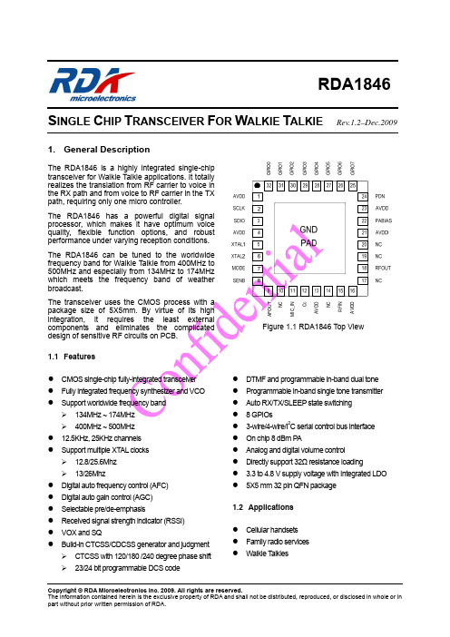
RDA1846S INGLE C HIP T RANSCEIVER F OR W ALKIE T ALKIE Rev.1.2–Dec.20091. General DescriptionThe RDA1846 is a highly integrated single-chip transceiver for Walkie Talkie applications. It totally realizes the translation from RF carrier to voice in the RX path and from voice to RF carrier in the TX path, requiring only one micro controller.The RDA1846 has a powerful digital signal processor, which makes it have optimum voice quality, flexible function options, and robust performance under varying reception conditions. The RDA1846 can be tuned to the worldwide frequency band for Walkie Talkie from 400MHz to 500MHz and especially from 134MHz to 174MHz which meets the frequency band of weather broadcast.The transceiver uses the CMOS process with a package size of 5X5mm. By virtue of its high integration, it requires the least external components and eliminates the complicated design of sensitive RF circuits on PCB.1.1 Features● CMOS single-chip fully-integrated transceiver ● Fully integrated frequency synthesizer and VCO ● Support worldwide frequency band134MHz ~ 174MHz 400MHz ~ 500MHz ● 12.5KHz, 25KHz channels ● Support multiple XTAL clocks12.8/25.6Mhz 13/26Mhz● Digital auto frequency control (AFC) ● Digital auto gain control (AGC) ● Selectable pre/de-emphasis ● Received signal strength indicator (RSSI) ● VOX and SQ● Build-in CTCSS/CDCSS generator and judgmentCTCSS with 120/180 /240 degree phase shift 23/24 bit programmable DCS code● DTMF and programmable in-band dual tone ● Programmable in-band single tone transmitter ● Auto RX/TX/SLEEP state switching ● 8 GPIOs● 3-wire/4-wire/I 2C serial control bus interface ● On chip 8 dBm P A● Analog and digital volume control ● Directly support 32Ω resistance loading ● 3.3 to 4.8 V supply voltage with Integrated LDO ● 5X5 mm 32 pin QFN package 1.2 Applications ● Cellularhandsets ● Family radio services ● Walkie T alkiesA F O U TN CM I C _I NA V D DN CR F I NA V DDC cG P I O 0G P I O 1G P I O 2G P I O 3G P I O 4G P I O 5G P I O 6G P I O 7Figure 1.1 RDA1846 Top View2. Table of Contents1.General Description (1)1.1Features (1)1.2Applications (1)2.Table of Contents (2)3.Functional Description (3)3.1RF input and output (3)3.2Voice input and output (4)3.3Synthesizer (4)3.4XTAL Clock (4)3.5DSP functions (4)3.6Integrated LDO (4)3.7Serial Control Interface (4)4.Electrical Characteristics (5)5.Receiver/Transmitter Characteristics (6)6.Control Interface Characteristics (7)7.Pins Description (8)8.Application Diagram (11)9.Package Outline (12)10.Solder Mounting Condition (13)11.Change List (16)12.Contact Information (16)3. Functional Description…Figure 3.1 RDA1846 Block DiagramThe RDA1846 transceiver features very low solution cost and reduced complexity. As shown in Fig.3.1, to totally complete the translation from RF carrier to voice in the RX path and from voice to RF carrier in the TX path, the chip integrates nearly all the functional blocks including RF and base band analog blocks and digital signal processor. It requires only one micro controller and a few external components to realize a walkie-talkie.A powerful integrated DSP accomplishes both the demodulation and modulation of the FM signal. Besides, standard walkie-talkie features such as CTS, CDS, VOX and SQ etc. are provided through the 8 GPIOs of the chip. Especially, by virtue of the state-of-the-art CMOS technology advanced algorithms such as AFC, AGC, RSSI and SNR calculations are realized in the DSP, which guarantees the high receiving and transmitting quality while still consumes a low power. Flexible RX/TX/SLEEP auto switching function from the DSP further reduces the average power consumptions.LDOs are also integrated in the chip which further reduces the BOMs.All interface pins of the chip will be shortly explained below. For details, refer to the ‘RDA 1846 programming guide’.3.1 RF input and outputThe chip can receive and transmit RF signals from 400 to 500MHz and from 134 to 174MHz which cover most of the walkie-talkie frequency bands around the world and the weather broadcast band. For the RF input, a direct-in connection from the antenna to the LNA input pin through a switch is suggested which means no input impedance matching is needed for the receive band. For the RF out, a pa diver can deliver no more than 8 dBm power to PA. PA bias voltage from 1.5V~2.8V for the power amplifier can be supplied from the PABIAS pin.3.2 Voice input and outputIn the RX path, the voice signal after demodulation is sent to the internal DAC which can directly drive a 32Ω resistance loading through AC coupling. In the TX path, microphone signal can be sent into the chip through AC coupling capacitors.3.3 SynthesizerThe frequency synthesizer generates the local oscillator signal. All building blocks are fully integrated without any external components. LO frequency can be programmed through the serial interface by the MCU. (How to select frequency band and program LO frequency, refer to the programming guide)3.4 XTAL ClockThe RDA1846 supports XT AL clocks such as 12.8 MHz, 13 MHz, 25.6 MHz and 26 MHz. The internal XTAL oscillator can also be bypassed thus TCXO clock with appropriate amplitude can be sent into the chip directly. (How to configure the internal XTAL oscillator, refer to the programming guide)3.5 DSP functionsThe DSP accomplishes the demodulation and modulation of the FM signal. Standard walkie-talkie features such as CTS, CDS, VOX and SQ etc. are provided through the 8 GPIOs. (How to configure theGPIOs, refer to the programming guide)3.6 Integrated LDOLDOs are integrated on chip which eliminates using one LDO chip on the PCB. Supply voltage for the chip is suggested to be within 3.3V~4.8V. A common share of the supply voltage for RDA1846 and other chips or on board circuits are not appropriate and thus not recommended.3.7 Serial Control InterfaceA 3-wire/4-wire/I2C serial interface is provided for host IC to read and write RDA1846 control registers. (For details of the serial control interface, refer to the programming guide).4. Electrical CharacteristicsTable 4-1 DC Electrical Specification (Recommended Operation Conditions): SYMBOL DESCRIPTION MIN TYP MAX UNITAVDD Supply Voltage from battery or LDO 3.3 3.3 4.8 VT amb Ambient Temperature -25 27 +85 ℃V L CMOS Low Level Input/output Voltage 0 0.3 VV H CMOS High Level Input/output Voltage 2.7 3 VV TH CMOSVoltage 1.5 V ThresholdTable 4-2 DC Electrical Specification (Absolute Maximum Ratings):SYMBOL DESCRIPTION MIN TYP MAX UNITT amb Ambient Temperature -40 +90 °CI IN Input Current-10 +10 mAV IN Input Voltage -0.3 3.3 VV lna LNA Input Level +10 dBmTable 4-3 Power consumption specification(AVDD = 3.3 V, T A = -25 to 85℃, unless otherwise specified)STATE DESCRIPTION Condition TYP UNITIContinue Receive RXON=1,PDN=1 55 mAI Tx Continue Transmit TXON=1,PDN=1 50 mAI sleep Deep sleep PDN=0 40 A5. Receiver/Transmitter CharacteristicsTable 5-1 Receiver Characteristics(AVDD = 3.3 V, TA = -25 to 85 °C, unless otherwise specified)SYMBOL PARAMETER CONDITIONS MIN TYP MAX UNIT General specificationsFin Input Frequency Range1 400 520 MHz Input Frequency Range2 134 174 MHzInput Frequency Range3 200 260 MHz NF Noise Figure Max RX Gain 3 dB IP3in Input IP3 Max RX Gain -10 -6 0 dBmSEN Sensitivity 12.5kHz channel,12dB SINAD-125 -124 -123 dBmACS Adjacent Channel Selectivity±12.5KHz 65 66 67 dBIR Image rejection 60 70 dBBlocker >1MHz 85 dB Voice distortion 1.5 %Table 5-2 Transmit Characteristics(AVDD = 3.3 V, TA = -25 to 85°C, unless otherwise specified)SYMBOL PARAMETER CONDITIONS MIN TYP MAX UNITGeneral specificationsFout Output Frequency Range1400 520 MHzOutput Frequency Range2134 174 MHzOutput Frequency Range3200 260 MHzPOUT Output Power -2 5 8 dBmSINAD/SNR 48/53dB ACP Adjacent channel power-67 dBcModulation sensitivity 1.5kHz frequency offset13 mVVoice distortion 0.5 %Modulation limitation 2.2 2.5 kHz6. Control Interface Characteristics Refer to the ‘RDA1846 programming guide’.7. Pins DescriptionFigure 7.1 RDA1846 Top ViewTable 7-1 RDA1846 Pins DescriptionSYMBOLPINDESCRIPTIONAVDD 1 Power supply SCLK 2 Clock input for serial control bus SDIO 3 Data input/output for serial control bus AVDD 4 Power supplyXTAL1 5 Oscillator pin 1 XTAL26Oscillator pin 2MODE 7 Control Interface selectWhen MODE = V L , I 2C Interface is selectWhen MODE = V H , SPI Interface is selectSENB 8 Latch enable (active low) input for serial control bus AFOUT9Audio signal output to speakerNC* 10 No connection MIC_IN 11 MIC input Cc12Compensation capacitor connection pinAVDD 13 Power supply NC* 14 No connection RFIN15RF signal inputAVDD 16 Power supply NC* 17 No connection RFOUT18RF signal outputNC* 19 No connection NC* 20 No connection AVDD 21 Power supply PABIAS 22 PA bias supply for PA AVDD 23 Power supply PDN24Chip enable, low activeGPIO7 25Gpio7 / vox (When Gpio7=V H , vox is active; else V L ) GPIO6 26Gpio6 / sq(When Gpio6=V H , sq is active; else V L ) GPIO5 27Gpio5 / txon(When Gpio5=V H , txon is active; else V L ) GPIO4 28Gpio4 / rxon(When Gpio4=V H , rxon is active; else V L )GPIO3 29 Gpio3 / sdo(Gpio3=V H or V L , it is the output register data in 4 wire controlinterface mode)GPIO2 30Gpio2 / int(When Gpio2=V H , int is active; else V L )GPIO1 31Gpio1 / code_in / code_out(Gpio1=V H or V L , it is the input/output code data)GPIO0 32Gpio0 / css_in / css_out(Gpio0=V H or V L , it is the input/output CTCSS/CDCSS signal)*Attention: all NC pins should be floating. Do not connect it to GND!8. Application DiagramFigure 8.1 RDA1846 Application DiagramNotes:RDA1846Chip;1 U1:2 AVDD: Power Supply for RDA1846 (3.3~4.8V);3 AVDD_PA: Power Supply for RF PA, its voltage depends on the actual PA design;4 C0~C11: AVDD decouple capacitance (1nF and 100nF in pairs), as close to AVDD pin as possible;5 CA1~CA2: Audio AC couple capacitance (~47uF);6 Cc: Compensation capacitance connected between pin Cc and GND (~47uF);7 Crf: RF AC couple capacitance (~150pF);8 CX1~CX2: XTAL oscillator load capacitance. Its value depends on the chosen XTAL (if using external TCXO, clkshould be sent into pin XTAL1 with Vpp about 1.5V, and pin XTAL2 should be connected to GND);9 R0~R1(optional): resistors for serial interface wire SDIO and SCLK (~10kΩ);10 Pins NC(10,14,17,19,20) should be floating;11 External vox detection circuit is optional;9. Package Outline32-Pin 5x5 Quad Flat No-Lead (QFN)10. Solder Mounting ConditionClassification Reflow ProfileTable 10-1 Classification Reflow ProfilesProfile Feature Sn-Pb Eutectic Assembly Pb-Free Assembly Average Ramp-Up Rate(T Smax to T p)3 o C/second max. 3 o C/second max.Preheat-Temperature Min (T smin)-Temperature Max (T smax)-Time (t smin to t smax)100 o C100 o C60-120 seconds150 o C200 o C60-180 seconds Time maintained above:-Temperature (T L)-Time (t L)183 o C60-150seconds217o C60-150 seconds Peak /ClassificationTemperature(T p)See Table-II See Table-IIITime within 5 o C of actualPeak Temperature (t p)10-30 seconds 20-40 seconds Ramp-Down Rate 6 o C/second max. 6 o C/seconds max.Time 25 o C to PeakTemperature6 minutes max. 8 minutes max.Table 10-2 SnPb Eutectic Process – Package Peak Reflow TemperaturesPackage Thickness Volume mm3<350Volume mm3≥350<2.5mm 240 + 0/-5 o C 225 + 0/-5 o C ≥2.5mm225 + 0/-5 o C225 + 0/-5 o CTable 10-3 Pb-free Process – Package Classification Reflow TemperaturesPackage Thickness Volume mm3<350Volume mm3350-2000Volume mm3>2000<1.6mm 260 + 0 o C * 260 + 0 o C *260 + 0 o C *1.6mm –2.5mm 260 + 0 o C *250 + 0 o C *245 + 0 o C *≥2.5mm250 + 0 o C *245 + 0 o C *245 + 0 o C * *Tolerance : The device manufacturer/supplier shall assure process compatibility up to and including the stated classification temperature(this mean Peak reflow temperature + 0 o C. Forexample 260+ 0 o C ) at the rated MSL Level.Note 1: All temperature refer topside of the package. Measured on the package body surface.Note 2: The profiling tolerance is + 0 o C, - X o C (based on machine variation capability)whatever is required to control the profile process but at no time will it exceed - 5 o C. The producer assures process compatibility at the peak reflow profile temperatures defined in Table –III. Note 3: Package volume excludes external terminals(balls, bumps, lands, leads) and/or non integral heat sinks.Note 4: The maximum component temperature reached during reflow depends on package the thickness and volume. The use of convection reflow processes reduces the thermal gradients between packages. However, thermal gradients due to differences in thermal mass of SMD package may sill exist.Note 5: Components intended for use in a “lead-free” assembly process shall be evaluated using the “lead free” classification temperatures and profiles defined in Table-I II III whether or not lead free.RoHS CompliantThe product does not contain lead, mercury, cadmium, hexavalent chromium, polybrominated biphenyls (PBB) or polybrominated diphenyl ethers (PBDE), and are therefore considered RoHS compliant.ESD SensitivityIntegrated circuits are ESD sensitive and can be damaged by static electricity. Proper ESD techniques should be used when handling these devices.11. Change ListREV DATE AUTHER CHANGE DESCRIPTION v1.0e 2009-06-24 Hao Shi Original draft.v1.1e 2009-10-10 Ge Liu V1.1 original draftv1.2e 2009-12-11 Ge Liu Add 200M~260MHz12. Contact InformationRDA Microelectronics (Shanghai), Inc.Suite 1108 Block A, e-Wing Center, 113 Zhichun Road Haidian District, BeijingTel: 86-10-62635360Fax: 86-10-82612663Postal Code: 100086。
I2C总线协议规范 v2.1
THE I2C-BUS SPECIFICATIONVERSION 2.1JANUARY 2000CONTENTS1PREFACE. . . . . . . . . . . . . . . . . . . . . . . . . . .3 1.1Version 1.0 - 1992. . . . . . . . . . . . . . . . . . . . 3 1.2Version 2.0 - 198. . . . . . . . . . . . . . . . . . . . . 3 1.3Version 2.1 - 1999. . . . . . . . . . . . . . . . . . . . 3 1.4Purchase of Philips I2C-bus components . . 3 2THE I2C-BUS BENEFITS DESIGNERSAND MANUFACTURERS. . . . . . . . . . . . . . .4 2.1Designer benefits . . . . . . . . . . . . . . . . . . . . 4 2.2Manufacturer benefits. . . . . . . . . . . . . . . . . 6 3INTRODUCTION TO THE I2C-BUSSPECIFICATION . . . . . . . . . . . . . . . . . . . . .6 4THE I2C-BUS CONCEPT . . . . . . . . . . . . . . .6 5GENERAL CHARACTERISTICS . . . . . . . . .8 6BIT TRANSFER . . . . . . . . . . . . . . . . . . . . . .8 6.1Data validity . . . . . . . . . . . . . . . . . . . . . . . . 8 6.2START and STOP conditions. . . . . . . . . . . 9 7TRANSFERRING DATA. . . . . . . . . . . . . . .10 7.1Byte format . . . . . . . . . . . . . . . . . . . . . . . . 10 7.2Acknowledge. . . . . . . . . . . . . . . . . . . . . . . 10 8ARBITRATION AND CLOCKGENERATION . . . . . . . . . . . . . . . . . . . . . .11 8.1Synchronization . . . . . . . . . . . . . . . . . . . . 11 8.2Arbitration . . . . . . . . . . . . . . . . . . . . . . . . . 12 8.3Use of the clock synchronizingmechanism as a handshake. . . . . . . . . . . 13 9FORMATS WITH 7-BIT ADDRESSES. . . .13 107-BIT ADDRESSING . . . . . . . . . . . . . . . . .15 10.1Definition of bits in the first byte . . . . . . . . 15 10.1.1General call address. . . . . . . . . . . . . . . . . 16 10.1.2START byte . . . . . . . . . . . . . . . . . . . . . . . 17 10.1.3CBUS compatibility. . . . . . . . . . . . . . . . . . 18 11EXTENSIONS TO THE STANDARD-MODE I2C-BUS SPECIFICATION . . . . . . .19 12FAST-MODE. . . . . . . . . . . . . . . . . . . . . . . .19 13Hs-MODE . . . . . . . . . . . . . . . . . . . . . . . . . .20 13.1High speed transfer. . . . . . . . . . . . . . . . . . 20 13.2Serial data transfer format in Hs-mode. . . 21 13.3Switching from F/S- to Hs-mode andback . . . . . . . . . . . . . . . . . . . . . . . . . . . . . 2313.4Hs-mode devices at lower speed modes. . 24 13.5Mixed speed modes on one serial bussystem. . . . . . . . . . . . . . . . . . . . . . . . . . . . 24 13.5.1F/S-mode transfer in a mixed-speed bussystem. . . . . . . . . . . . . . . . . . . . . . . . . . . . 25 13.5.2Hs-mode transfer in a mixed-speed bussystem. . . . . . . . . . . . . . . . . . . . . . . . . . . . 25 13.5.3Timing requirements for the bridge in amixed-speed bus system. . . . . . . . . . . . . . 27 1410-BIT ADDRESSING. . . . . . . . . . . . . . . . 27 14.1Definition of bits in the first two bytes. . . . . 27 14.2Formats with 10-bit addresses. . . . . . . . . . 27 14.3General call address and start byte with10-bit addressing. . . . . . . . . . . . . . . . . . . . 30 15ELECTRICAL SPECIFICATIONSAND TIMING FOR I/O STAGESAND BUS LINES. . . . . . . . . . . . . . . . . . . . 30 15.1Standard- and Fast-mode devices. . . . . . . 30 15.2Hs-mode devices. . . . . . . . . . . . . . . . . . . . 34 16ELECTRICAL CONNECTIONS OFI2C-BUS DEVICES TO THE BUS LINES . 37 16.1Maximum and minimum values ofresistors R p and R s for Standard-modeI2C-bus devices . . . . . . . . . . . . . . . . . . . . . 39 17APPLICATION INFORMATION. . . . . . . . . 41 17.1Slope-controlled output stages ofFast-mode I2C-bus devices. . . . . . . . . . . . 41 17.2Switched pull-up circuit for Fast-modeI2C-bus devices . . . . . . . . . . . . . . . . . . . . . 41 17.3Wiring pattern of the bus lines. . . . . . . . . . 42 17.4Maximum and minimum values ofresistors R p and R s for Fast-modeI2C-bus devices . . . . . . . . . . . . . . . . . . . . . 42 17.5Maximum and minimum values ofresistors R p and R s for Hs-modeI2C-bus devices . . . . . . . . . . . . . . . . . . . . . 42 18BI-DIRECTIONAL LEVEL SHIFTERFOR F/S-MODE I2C-BUS SYSTEMS . . . . 42 18.1Connecting devices with differentlogic levels. . . . . . . . . . . . . . . . . . . . . . . . . 43 18.1.1Operation of the level shifter . . . . . . . . . . . 44 19DEVELOPMENT TOOLS AVAILABLEFROM PHILIPS. . . . . . . . . . . . . . . . . . . . . 45 20SUPPORT LITERATURE . . . . . . . . . . . . . 461PREFACE1.1Version 1.0 - 1992This version of the 1992 I2C-bus specification includes the following modifications:•Programming of a slave address by software has been omitted. The realization of this feature is rather complicated and has not been used.•The “low-speed mode” has been omitted. This mode is, in fact, a subset of the total I2C-bus specification and need not be specified explicitly.•The Fast-mode is added. This allows a fourfold increase of the bit rate up to 400kbit/s. Fast-mode devices are downwards compatible i.e. they can be used in a 0 to 100kbit/s I2C-bus system.•10-bit addressing is added. This allows 1024 additional slave addresses.•Slope control and input filtering for Fast-mode devices is specified to improve the EMC behaviour.NOTE: Neither the 100kbit/s I2C-bus system nor the 100kbit/s devices have been changed.1.2Version2.0 - 1998The I2C-bus has become a de facto world standard that is now implemented in over 1000 different ICs and licensed to more than 50 companies. Many of today’s applications, however, require higher bus speeds and lower supply voltages. This updated version of the I2C-bus specification meets those requirements and includes the following modifications:•The High-speed mode (Hs-mode) is added. This allows an increase in the bit rate up to 3.4Mbit/s. Hs-mode devices can be mixed with Fast- and Standard-mode devices on the one I2C-bus system with bit rates from 0 to 3.4Mbit/s.•The low output level and hysteresis of devices with a supply voltage of 2V and below has been adapted to meet the required noise margins and to remain compatible with higher supply voltage devices.•The 0.6V at 6mA requirement for the output stages of Fast-mode devices has been omitted.•The fixed input levels for new devices are replaced by bus voltage-related levels.•Application information for bi-directional level shifter is added.1.3Version2.1 - 2000Version 2.1 of the I2C-bus specification includes the following minor modifications:•After a repeated START condition in Hs-mode, it is possible to stretch the clock signal SCLH (see Section13.2 and Figs22, 25 and 32).•Some timing parameters in Hs-mode have been relaxed (see Tables6 and 7).1.4Purchase of Philips I2C-bus componentsPurchase of Philips I2C components conveys a license under the Philips’ I2C patent to use thecomponents in the I2C system provided the system conforms to the I2C specification defined byPhilips.2THE I2C-BUS BENEFITS DESIGNERS AND MANUFACTURERSIn consumer electronics, telecommunications and industrial electronics, there are often many similarities between seemingly unrelated designs. For example, nearly every system includes:•Some intelligent control, usually a single-chip microcontroller•General-purpose circuits like LCD drivers, remote I/O ports, RAM, EEPROM, or data converters•Application-oriented circuits such as digital tuning and signal processing circuits for radio and video systems, or DTMF generators for telephones with tone dialling.To exploit these similarities to the benefit of both systems designers and equipment manufacturers, as well as to maximize hardware efficiency and circuit simplicity, Philips developed a simple bi-directional 2-wire bus for efficient inter-IC control. This bus is called the Inter IC or I2C-bus. At present, Philips’ IC range includes more than 150 CMOS and bipolar I2C-bus compatible types for performing functions in all three of the previously mentioned categories. All I2C-bus compatible devices incorporate an on-chip interface which allows them to communicate directly with each other via the I2C-bus. This design concept solves the many interfacing problems encountered when designing digital control circuits.Here are some of the features of the I2C-bus:•Only two bus lines are required; a serial data line (SDA) and a serial clock line (SCL)•Each device connected to the bus is software addressable by a unique address and simplemaster/slave relationships exist at all times; masters can operate as master-transmitters or as master-receivers•It’s a true multi-master bus including collision detection and arbitration to prevent data corruption if two or more masters simultaneously initiate data transfer•Serial, 8-bit oriented, bi-directional data transfers can be made at up to 100kbit/s in the Standard-mode, up to 400kbit/s in the Fast-mode, or up to 3.4Mbit/s in the High-speed mode•On-chip filtering rejects spikes on the bus data line to preserve data integrity •The number of ICs that can be connected to the same bus is limited only by a maximum bus capacitance of 400pF.Figure1 shows two examples of I2C-bus applications. 2.1Designer benefitsI2C-bus compatible ICs allow a system design to rapidly progress directly from a functional block diagram to a prototype. Moreover, since they ‘clip’ directly onto theI2C-bus without any additional external interfacing, they allow a prototype system to be modified or upgraded simply by ‘clipping’ or ‘unclipping’ ICs to or from the bus. Here are some of the features of I2C-bus compatible ICs which are particularly attractive to designers:•Functional blocks on the block diagram correspond with the actual ICs; designs proceed rapidly from block diagram to final schematic.•No need to design bus interfaces because the I2C-bus interface is already integrated on-chip.•Integrated addressing and data-transfer protocol allow systems to be completely software-defined•The same IC types can often be used in many different applications•Design-time reduces as designers quickly become familiar with the frequently used functional blocks represented by I2C-bus compatible ICs•ICs can be added to or removed from a system without affecting any other circuits on the bus•Fault diagnosis and debugging are simple; malfunctions can be immediately traced•Software development time can be reduced by assembling a library of reusable software modules.In addition to these advantages, the CMOS ICs in theI2C-bus compatible range offer designers special features which are particularly attractive for portable equipment and battery-backed systems.They all have:•Extremely low current consumption•High noise immunity•Wide supply voltage range•Wide operating temperature range.Fig.1 Two examples of I 2C-bus applications: (a) a high performance highly-integrated TV set(b) DECT cordless phone base-station.handbook, full pagewidthSDA SCLMICRO-CONTROLLER PCB83C528PLLSYNTHESIZERTSA5512NON-VOLATILE MEMORY PCF8582ESTEREO / DUAL SOUND DECODER TDA9840HI-FI AUDIOPROCESSOR TDA9860SINGLE-CHIP TEXT SAA52XXM/S COLOUR DECODER TDA9160APICTURE SIGNALIMPROVEMENTTDA4670VIDEOPROCESSORTDA4685ON-SCREENDISPLAYPCA8510(a)MSB575SDASCLLINEINTERFACEPCA1070BURST MODE CONTROLLERPCD5042ADPCMPCD5032(b)DTMFGENERATOR PCD3311MICRO-CONTROLLER P80CLXXX2.2Manufacturer benefitsI2C-bus compatible ICs don’t only assist designers, they also give a wide range of benefits to equipment manufacturers because:•The simple 2-wire serial I2C-bus minimizes interconnections so ICs have fewer pins and there are not so many PCB tracks; result - smaller and less expensive PCBs•The completely integrated I2C-bus protocol eliminates the need for address decoders and other ‘glue logic’•The multi-master capability of the I2C-bus allows rapid testing and alignment of end-user equipment via external connections to an assembly-line•The availability of I2C-bus compatible ICs in SO (small outline), VSO (very small outline) as well as DIL packages reduces space requirements even more. These are just some of the benefits. In addition, I2C-bus compatible ICs increase system design flexibility by allowing simple construction of equipment variants and easy upgrading to keep designs up-to-date. In this way, an entire family of equipment can be developed around a basic model. Upgrades for new equipment, or enhanced-feature models (i.e. extended memory, remote control, etc.) can then be produced simply by clipping the appropriate ICs onto the bus. If a larger ROM is needed, it’s simply a matter of selecting a micro-controller with a larger ROM from our comprehensive range. As new ICs supersede older ones, it’s easy to add new features to equipment or to increase its performance by simply unclipping the outdated IC from the bus and clipping on its successor.3INTRODUCTION TO THE I2C-BUS SPECIFICATION For 8-bit oriented digital control applications, such as those requiring microcontrollers, certain design criteria can be established:•A complete system usually consists of at least one microcontroller and other peripheral devices such as memories and I/O expanders•The cost of connecting the various devices within the system must be minimized •A system that performs a control function doesn’t require high-speed data transfer•Overall efficiency depends on the devices chosen and the nature of the interconnecting bus structure.To produce a system to satisfy these criteria, a serial bus structure is needed. Although serial buses don’t have the throughput capability of parallel buses, they do require less wiring and fewer IC connecting pins. However, a bus is not merely an interconnecting wire, it embodies all the formats and procedures for communication within the system.Devices communicating with each other on a serial bus must have some form of protocol which avoids all possibilities of confusion, data loss and blockage of information. Fast devices must be able to communicate with slow devices. The system must not be dependent on the devices connected to it, otherwise modifications or improvements would be impossible. A procedure has also to be devised to decide which device will be in control of the bus and when. And, if different devices with different clock speeds are connected to the bus, the bus clock source must be defined. All these criteria are involved in the specification of the I2C-bus.4THE I2C-BUS CONCEPTThe I2C-bus supports any IC fabrication process (NMOS, CMOS, bipolar). Two wires, serial data (SDA) and serial clock (SCL), carry information between the devices connected to the bus. Each device is recognized by a unique address (whether it’s a microcontroller, LCD driver, memory or keyboard interface) and can operate as either a transmitter or receiver, depending on the function of the device. Obviously an LCD driver is only a receiver, whereas a memory can both receive and transmit data. In addition to transmitters and receivers, devices can also be considered as masters or slaves when performing data transfers (see Table 1). A master is the device which initiates a data transfer on the bus and generates the clock signals to permit that transfer. At that time, any device addressed is considered a slave.Table 1Definition of I 2C-bus terminologyThe I 2C-bus is a multi-master bus. This means that more than one device capable of controlling the bus can be connected to it. As masters are usually micro-controllers, let’s consider the case of a data transfer between two microcontrollers connected to the I 2C-bus (see Fig.2). This highlights the master-slave and receiver-transmitter relationships to be found on the I 2C-bus. It should be noted that these relationships are not permanent, but onlydepend on the direction of data transfer at that time. The transfer of data would proceed as follows:1) Suppose microcontroller A wants to send information to microcontroller B:•microcontroller A (master), addresses microcontroller B (slave)•microcontroller A (master-transmitter), sends data to microcontroller B (slave- receiver)•microcontroller A terminates the transfer2) If microcontroller A wants to receive information from microcontroller B:•microcontroller A (master) addresses microcontroller B (slave)•microcontroller A (master- receiver) receives data from microcontroller B (slave- transmitter)•microcontroller A terminates the transfer.Even in this case, the master (microcontroller A) generates the timing and terminates the transfer.The possibility of connecting more than onemicrocontroller to the I 2C-bus means that more than one master could try to initiate a data transfer at the same time. To avoid the chaos that might ensue from such an event - an arbitration procedure has been developed. Thisprocedure relies on the wired-AND connection of all I 2C interfaces to the I 2C-bus.If two or more masters try to put information onto the bus, the first to produce a ‘one’ when the other produces a ‘zero’ will lose the arbitration. The clock signals during arbitration are a synchronized combination of the clocks generated by the masters using the wired-AND connection to the SCL line (for more detailed information concerning arbitration see Section 8).TERM DESCRIPTIONT ransmitter The device which sends data to the busReceiver The device which receives data from the busMasterThe device which initiates a transfer, generates clock signals and terminates a transferSlave The device addressed by a master Multi-masterMore than one master can attempt to control the bus at the same time without corrupting the message ArbitrationProcedure to ensure that, if more than one master simultaneously tries to control the bus, only one is allowed to do so and the winning message is not corruptedSynchronizationProcedure to synchronize the clock signals of two or more devicesFig.2 Example of an I 2C-bus configuration using two microcontrollers.MBC645SDA SCLMICRO -CONTROLLER ASTATIC RAM OR EEPROMLCD DRIVERGATE ARRAYADCMICRO -CONTROLLER BGeneration of clock signals on the I 2C-bus is always the responsibility of master devices; each master generates its own clock signals when transferring data on the bus. Bus clock signals from a master can only be altered when they are stretched by a slow-slave device holding-down the clock line, or by another master when arbitration occurs.5GENERAL CHARACTERISTICSBoth SDA and SCL are bi-directional lines, connected to a positive supply voltage via a current-source or pull-up resistor (see Fig.3). When the bus is free, both lines are HIGH. The output stages of devices connected to the bus must have an open-drain or open-collector to perform the wired-AND function. Data on the I 2C-bus can be transferred at rates of up to 100kbit/s in theStandard-mode, up to 400kbit/s in the Fast-mode, or up to 3.4Mbit/s in the High-speed mode. The number ofinterfaces connected to the bus is solely dependent on the bus capacitance limit of 400pF. For information on High-speed mode master devices, see Section 13.6BIT TRANSFERDue to the variety of different technology devices (CMOS, NMOS, bipolar) which can be connected to the I 2C-bus, the levels of the logical ‘0’ (LOW) and ‘1’ (HIGH) are not fixed and depend on the associated level of V DD (see Section 15 for electrical specifications). One clock pulse is generated for each data bit transferred.6.1Data validityThe data on the SDA line must be stable during the HIGH period of the clock. The HIGH or LOW state of the data line can only change when the clock signal on the SCL line is LOW (see Fig.4).Fig.3 Connection of Standard- and Fast-mode devices to the I 2C-bus.MBC631SCLKN1OUT SCLK INSCLKDATAN1OUT DATA IN DEVICE 1SDA (Serial Data Line)SCL (Serial Clock Line)SCLKN2OUT SCLK INSCLK DATAN2OUT DATA IN DEVICE 2V DDR pR ppull-up resistorsFig.4 Bit transfer on the I 2C-bus.handbook, full pagewidthMBC621data line stable;data validchange of data allowedSDASCL6.2START and STOP conditionsWithin the procedure of the I 2C-bus, unique situations arise which are defined as START (S) and STOP (P) conditions (see Fig.5).A HIGH to LOW transition on the SDA line while SCL is HIGH is one such unique case. This situation indicates a START condition.A LOW to HIGH transition on the SDA line while SCL is HIGH defines a STOP condition.START and STOP conditions are always generated by the master. The bus is considered to be busy after the START condition. The bus is considered to be free again a certain time after the STOP condition. This bus free situation is specified in Section 15.The bus stays busy if a repeated START (Sr) is generated instead of a STOP condition. In this respect, the START (S) and repeated START (Sr) conditions are functionally identical (see Fig. 10). For the remainder of this document, therefore, the S symbol will be used as a generic term to represent both the START and repeated START conditions, unless Sr is particularly relevant.Detection of START and STOP conditions by devices connected to the bus is easy if they incorporate the necessary interfacing hardware. However,microcontrollers with no such interface have to sample the SDA line at least twice per clock period to sense the transition.Fig.5 START and STOP conditions.handbook, full pagewidthMBC622SDA SCLPSTOP conditionSDASCLSSTART condition7TRANSFERRING DATA 7.1Byte formatEvery byte put on the SDA line must be 8-bits long. The number of bytes that can be transmitted per transfer is unrestricted. Each byte has to be followed by an acknowledge bit. Data is transferred with the most significant bit (MSB) first (see Fig.6). If a slave can’t receive or transmit another complete byte of data until it has performed some other function, for example servicing an internal interrupt, it can hold the clock line SCL LOW to force the master into a wait state. Data transfer thencontinues when the slave is ready for another byte of data and releases clock line SCL.In some cases, it’s permitted to use a different format from the I 2C-bus format (for CBUS compatible devices for example). A message which starts with such an address can be terminated by generation of a STOP condition, even during the transmission of a byte. In this case, no acknowledge is generated (see Section 10.1.3).7.2AcknowledgeData transfer with acknowledge is obligatory. The acknowledge-related clock pulse is generated by the master. The transmitter releases the SDA line (HIGH) during the acknowledge clock pulse.The receiver must pull down the SDA line during the acknowledge clock pulse so that it remains stable LOWduring the HIGH period of this clock pulse (see Fig.7). Of course, set-up and hold times (specified in Section 15) must also be taken into account.Usually, a receiver which has been addressed is obliged to generate an acknowledge after each byte has been received, except when the message starts with a CBUS address (see Section 10.1.3).When a slave doesn’t acknowledge the slave address (for example, it’s unable to receive or transmit because it’s performing some real-time function), the data line must be left HIGH by the slave. The master can then generate either a STOP condition to abort the transfer, or a repeated START condition to start a new transfer.If a slave-receiver does acknowledge the slave address but, some time later in the transfer cannot receive any more data bytes, the master must again abort the transfer. This is indicated by the slave generating thenot-acknowledge on the first byte to follow. The slave leaves the data line HIGH and the master generates a STOP or a repeated START condition.If a master-receiver is involved in a transfer, it must signal the end of data to the slave- transmitter by not generating an acknowledge on the last byte that was clocked out of the slave. The slave-transmitter must release the data line to allow the master to generate a STOP or repeated START condition.Fig.6 Data transfer on the I 2C-bus.handbook, full pagewidthMSC608Sr or PSDASrPSCLSTOP or repeated STARTconditionS or SrSTART or repeated STARTcondition12 3 - 89ACK9ACK7812MSBacknowledgement signal from slavebyte complete,interrupt within slaveclock line held low while interrupts are servicedacknowledgement signal from receiverFig.7 Acknowledge on the I 2C-bus.handbook, full pagewidthMBC602S START condition9821clock pulse for acknowledgementnot acknowledgeacknowledgeDATA OUTPUT BY TRANSMITTERDATA OUTPUT BY RECEIVERSCL FROM MASTER8ARBITRATION AND CLOCK GENERATION 8.1SynchronizationAll masters generate their own clock on the SCL line to transfer messages on the I 2C-bus. Data is only valid during the HIGH period of the clock. A defined clock is therefore needed for the bit-by-bit arbitration procedure to take place.Clock synchronization is performed using the wired-AND connection of I 2C interfaces to the SCL line. This meansthat a HIGH to LOW transition on the SCL line will cause the devices concerned to start counting off their LOW period and, once a device clock has gone LOW, it will hold the SCL line in that state until the clock HIGH state is reached (see Fig.8). However, the LOW to HIGH transition of this clock may not change the state of the SCL line if another clock is still within its LOW period. The SCL line will therefore be held LOW by the device with the longest LOW period. Devices with shorter LOW periods enter a HIGH wait-state during this time.Fig.8 Clock synchronization during the arbitration procedure.CLK 1CLK 2SCLcounter resetwait statestart counting HIGH periodMBC632When all devices concerned have counted off their LOW period, the clock line will be released and go HIGH. There will then be no difference between the device clocks and the state of the SCL line, and all the devices will start counting their HIGH periods. The first device to complete its HIGH period will again pull the SCL line LOW.In this way, a synchronized SCL clock is generated with its LOW period determined by the device with the longest clock LOW period, and its HIGH period determined by the one with the shortest clock HIGH period.8.2ArbitrationA master may start a transfer only if the bus is free. Two or more masters may generate a START condition within the minimum hold time (t HD;STA ) of the START condition which results in a defined START condition to the bus.Arbitration takes place on the SDA line, while the SCL line is at the HIGH level, in such a way that the master which transmits a HIGH level, while another master istransmitting a LOW level will switch off its DATA output stage because the level on the bus doesn’t correspond to its own level.Arbitration can continue for many bits. Its first stage is comparison of the address bits (addressing information is given in Sections 10 and 14). If the masters are each tryingto address the same device, arbitration continues with comparison of the data-bits if they are master-transmitter, or acknowledge-bits if they are master-receiver. Because address and data information on the I 2C-bus is determined by the winning master, no information is lost during the arbitration process.A master that loses the arbitration can generate clock pulses until the end of the byte in which it loses the arbitration.As an Hs-mode master has a unique 8-bit master code, it will always finish the arbitration during the first byte (see Section 13).If a master also incorporates a slave function and it loses arbitration during the addressing stage, it’s possible that the winning master is trying to address it. The losingmaster must therefore switch over immediately to its slave mode.Figure 9 shows the arbitration procedure for two masters. Of course, more may be involved (depending on how many masters are connected to the bus). The moment there is a difference between the internal data level of the master generating DATA 1 and the actual level on the SDA line, its data output is switched off, which means that a HIGH output level is then connected to the bus. This will not affect the data transfer initiated by the winning master.Fig.9 Arbitration procedure of two masters.handbook, full pagewidthMSC609DATA 1DATA 2SDASCLSmaster 1 loses arbitrationDATA 1 SDA。
毕业设计(论文)-基于单片机的多功能钟控收音机的设计与实现--闹钟子系统的设计与实现[管理资料]
![毕业设计(论文)-基于单片机的多功能钟控收音机的设计与实现--闹钟子系统的设计与实现[管理资料]](https://img.taocdn.com/s3/m/93ab9c330c22590103029d9e.png)
基于单片机的多功能钟控收音机的设计与实现——闹钟子系统的设计与实现摘要收音机是现在生活中的一种娱乐工具,它可以扩展我们的知识面,丰富我们是日常生活。
但是现在的收音机仅仅只拥有收台、听台、存台的功能,功能上非常的单一,为了让收音机具有更强大的的功能,设计了这套基于单片机的多功能钟控收音机系统。
这套系统在传统的收音机上增加了时钟设置、温度测量、液晶显示以及闹钟设置多项功能。
本文主要论述了系统的方案设计,系统硬件设计包括硬件选型和硬件电路图;系统软件设计包括程序流程图设计和关键代码。
通过编写代码实现收音机节目的播放、音量调节、电台切换及节目的自动搜索、节目频点存储功能、时钟设置、温度测量、液晶显示以及闹钟功能。
且能够通过按键调整系统时钟,到达设定闹铃时间值可选择蜂鸣器响或开启收音机到指定频点。
该系统与传统的收音机系统相比较,具有结构简单,抗干扰能力强,测量精度高,使用方便的特点。
关键字:单片机;收音机;闹钟;液晶显示Based on SCM multi-function clock radio control design and realized ——Alarm subsystem of design and implementationAuthor:Li XinfangTutor:Yang BoAbstractThe radio is now in the life of the one kind of entertainment tool, it can expand our knowledge, enrich our daily life is. But now the radio only accept ,listen , save a function, the function is a single, in order to let the radio has more powerful function, the set design based on single chip microcomputer multifunctional clock radio control system. The system in the traditional radio increased the clock set, temperature measurement, liquid crystal display and alarm multiple functions. This paper discusses the design of the whole system, hardware design including hardware selection and hardware circuit diagram; System software design including program flowchart design and key code. By writing code realization of radio programs broadcast, volume adjustment, radio switch and programs to be automatic search, the program frequency memory function, clock set, temperature measurement, liquid crystal display and alarm clock function. And to be able to button to adjust the system clock, to set the alarm time value can choose a buzzer rang or open radio frequency to the specified. This system and the traditional radio system comparison, the structure is simple, strong anti-jamming ability, high accuracy, easy to use features.Key words: Single chip microcomputer; the radio; the alarm clock; liquid crystal display目录1 绪论 0 0研究的目的及意义 0本文结构 (1)2 系统方案设计 (2) (2) (2)收音机模块 (3)时钟模块 (3)温度模块 (3)显示模块 (3)闹钟模块 (3)按键模块 (4)3 系统硬件设计 (5) (5) (5)AT89S52单片机的引脚结构分析 (6)单片机最小系统设计图 (7)显示模块硬件电路设计 (7) (7)显示模块电路设计 (8)按键模块硬件电路设计 (8)时钟模块的硬件电路设计 (9) (9) (9) (10)存储模块硬件电路设计 (11) (11) (11)AT24C02电路设计 (12)打铃模块电路设计 (12)4 系统软件设计 (14)系统软件总体设计 (14)主控模块详细设计 (14)显示模块详细设计 (16)按键模块详细设计 (17)时钟模块详细设计 (18) (18)存储模块详细设计 (20) (21) (23)5系统的调试与实现 (25)C介绍 (25)6 结束语 (27)参考文献 (28)致谢 (29)1 绪论收音机一直在人们的生活娱乐中占有非常重要的地位。
KT0612音频接收芯片

Applications
Wireless Microphone, DVD player, Blue ray player, Set-top Box, Portable Device, Wireless Speaker
Rev.1.2
Information furnished by KT Micro is believed to be accurate and reliable. However, no responsibility is assumed by KT Micro for its use, nor for any infringements of patents or other rights of third parties which may result from its use. No license is granted by implication or otherwise under any patent or patent rights of Beijing KT Micro, Ltd.
RFINP LNA RFINN ADC AOUTP Audio DAC AOUTN
DSP Based FM demodulator & Audio processor
ADC
SCL I2C Master SDA Regulator Crystal
VDDVSSXI NhomakorabeaXO
KT0612 System Diagram
Description
The KT0612 is the VHF band chip of our full suite of the revolutionary wireless microphone chips, KT06xx, which replace hundreds of discrete components in a wireless microphone system while keeping the high standard of sound quality and functionality. The KT0612 is a VHF band receiver that includes audio amplifier, de-emphasis, expander, LO synthesizer and audio DAC. It is designed to process the modulated FM signal in VHF band and demodulate it into audio signal. The KT0612 only requires a single low-voltage supply thanks to a built-in regulator. For an audio transmission system built with a KT0612, no external tuning is required, which makes design-in effort minimum. The KT0612 provides direct and simple interface to support mechanical tuning. A pre-programmed low cost EEPROM can be used to configure the radio settings to differentiate product designs and accommodate standards in various regions. No external MCU is required. It is packaged in generic QFN24.
使用DMR和DSDPlus入门说明书

Andrew Milluzzi, KK4LWR125 SE 16th Ave., Apt L202, Gainesville, FL 32601; *******************Getting Started withDMR and DSDPlus This simple tutorial can help get you started on digital modulation.Digital modulations are becoming quitepopular in Amateur Radio. Technologies likeDMR, D-STAR, and System Fusion havemade the technology accessible and a newplatform for experimentation. Recently therewas much buzz about the Tytera MD-380,an inexpensive digital mobile radio (DMR)handheld transceiver. Technologies suchas the RTL-SDR — software defined radiobased on the RTL chip set — have broughtsoftware defined radio to the masses.C ombining these two technologies canenable additional experimentation.Recently the Gator Amateur RadioClub, W4DFU, at the University of Floridainstalled a DMR repeater for Gainesvilleand the surrounding area. This repeater is agreat resource for students and Technicianclass operators to talk all over the worldusing UHF locally. It is easy to get startedwith DMR by just listening to typical DMRcontacts. Depending on the talk group, someare quick, others are well organized nets. One option to decode DMR is to purchase a radio. Another is constructing a receiver from an RTL-SDR, an antenna, and some software.What is DMR?DMR stands for Digital Mobile Radio. Sometimes it is called MotoTURBO, the DMR product produced by Motorola Solutions. Like D-STAR or System Fusion, DMR digitizes voice using a vocoder and sends the information via digital packet. Unlike D-STAR and System Fusion, DMR uses TDMA (Time Division Multiple Access) with two time slots in 12.5 kHz. This enables one DMR repeater to act as two on a given frequency.What is DSDPlus?DSDPlus is an application that runs on aWindows computer that can decode multipledigital modes.1 Similar to the open sourceDSD program, DSDPlus takes an audiostream from a radio and can generate text oraudio. The main difference for the scope ofthis tutorial is that the open source programmust be compiled from source code, whileDSDPlus offers a Windows binary.Hardware SetupMy decoding setup requires just a fewpieces of physical hardware, seen in Figure1, and a some virtual hardware. The firstthing you need is a DMR source. I alreadyhad purchased a Tytera MD-380 handheldtransceiver, since I am quite interested inthe ongoing firmware experimentationcommunity. Y ou might already have a DMRsource, via other hams and perhaps a localrepeater. If you do decided to purchase aDMR radio, Motorola Solutions and Hyteraeach make some outstanding radios. BothC onnect Systems and Tytera make somemore inexpensive options.The second needed piece of hardware is aradio to connect to your computer. Y ou coulduse a VHF/UHF radio and a sound card tointerface with your computer. However, Iopted for an RTL-SDR for this project. AnRTL-SDR is essentially an inexpensive TVtuner USB dongle for your computer. Itcan be purchased for less than $20 and cancover 50 MHz to 1.7 GHz. Your Windows Figure 1 — DMR decoding setup using a Tytera MD-380 handheld transceiver, a laptop computer, and an RTL-SDR dongle. [Andy Milluzzi, KK4LWR, photo]QEX March/April 2017 1920 QEX March/April 2017operating system will most likely need a special driver to use the card as an SDR. Y ou can install the correct driver with assistance from the Zadig web page.2 The Zadig website has a simple guide for installing the WinUSB driver. This tutorial will assume you are using an RTL-SDR with the appropriate driver. The final needed hardware component for this tutorial is virtual. The DSD software needs a way to pass the audio. If you are using your computer sound card and an external radio, then you can skip this hardware. I recommend a VB-Audio Virtual Cable as a free solution.3 When you download and install the software, you should notice a new audio input and output device on your computer that acts as a sound card.Setting up DSDPlus SuiteDownload the latest version of DSDPlus and DSDPlus DLL package from the DSDPlus web page.4 Extract the contents of the DSDPlus zip file and the DLL zip file to a folder. Y ou should see a few dozen files. For this tutorial, we will focus on FMP-VC.bat and VC.bat. In DSDPlus two programs must be configured: FMP and DSDPlus. FMP is a basic narrowband FM tuner for an SDR. DSDPlus is the decoder.With all the files extracted, open a command prompt. In the Windows environment, this can be done by pressing the Windows key on your keyboard and typing C MD. Once open, navigate to the folder containing the DSDPlus files. Another option in Windows 8 or Windows 10 is to click on the File menu in your Explorer window. One of the options listed is open a command prompt. If done from the DSDPlus folder, you will not need to navigate.Setting up FMPOpen the file FMP-VC.bat. Y ou will see several parameters. Modify this script for our use by configuring the four parameters “–I”, “–o”, “–P”, and “–f”. The “–i” parameter followed by number (without a space) indicates which SDR to use as an input. For the SDR we can assume it is the only one on your computer, so set it to “–i1”. The “–o” parameter followed by a number is the output audio device. The “–P” parameter is the parts-per million (ppm) correction for your SDR. The “–f” parameter is the frequency in megahertz.To determine the values for the other parameters requires some knowledge about your setup. Let’s first tackle the output audio source. Each computer is different. The best way to determine the audio output is to observe what FMP sees. For this next part, you might find it helpful to unplug theSDR from the computer; if it is plugged inFigure 3 — Screen capture of FMP successfully running, controlling the SDR. Note thecommand prompt window showing the correct ppm correction and frequency.Figure 2 — Running FMP .EXE produces this text. Note the listed audio output devices.the program will launch. Type “FMP .EXE” in your command prompt window. Without an SDR plugged in, the application should fail to launch, but will still list the audio devices. For this program, we need to feed the output to our virtual audio port input. On my computer it is “Audio output device #2” seen in Figure 2.QEX March/April 2017 21Setting the ppm correction for your SDR is specific to your device. You can experiment by leaving it at 0.0. Alternatively you can use another SDR program such as SDR# from the AIRSPY web page to find the ppm correction.5 My device required a ppm correction of +75.The last parameter to set is the frequency to monitor. I do not want to clog the larger DMR network with my testing traffic, so I generated my own signals on 446.075 MHz, one of the UHF simplex frequency. DMR is mostly on UHF in the United States. Once the system is working, you can change the frequency to a local repeater.If done correctly, your FMP-VC.bat should look like:“FMP –i1 –o2 –P75 –f446.075”.Plug in your SDR tuner and run the script. Y ou should see several windows pop up. Y our computer screen should look like Figure 3. Save the changes to FMP-VC.bat. Y ou can close FMP by pressing the ESC key.Setting up DSDPlusC onfigure the DSDPlus script with a similar process. Open the VC.bat file and observe the various parameters. The parameters that start with a “w”:“–wsl”, “–wss”, “–wel”, and “–wcl”control where the windows are launched. Y ou can set these as you like.We must configure the audio as we did before by launching DSDPlus from our opencommand prompt. Unfortunately, there isFigure 5 — A screen capture of several windows of DSDPlus while decoding.Figure 4 — Running DSDPlus lists both input and output audio devices.no way to stop the program from opening all the windows, so you might need to move the various windows out of the way to see the command prompt and get your results. On my computer I got the results shown in Figure 4.The input should be set to the virtual audio cable output. The output must be your system speakers. In my case this results in input device #1 and output device #1 respectively. This enables me to hear anyone calling. A few other parameters must be set to make DMR work. The first parameter, “–rv”, tells DSDPlus that we expect voice. DSDPlus must also be set to decode DMR/MotoTURBO, since DSDPlus can do much more than just DMR — DSDPlus documentation indicates that it decodes D-STAR, except audio. It also can also decode P25 Phase 1 and NEXEDGE.To enable DMR we need to pass the “–fr” parameter. We also need to tell DSDPlus which of the two time slots we want tomonitor. This is done via passing “–1” or “–2” after the “–fr” parameter. Those are the only required parameters to make it work. You can record what DSDPlus decodes using the “–Pwav” parameter to save the audio as a wave file. Y ou might also discover a “–v3” parameter in the sample provided by DSDPlus. This enables verbose logging and I recommend using it, especially for debugging your scripts.When you are done, you should have a VC.bat script similar to:“DSDPlus –fr –1 –rv -Pwav –i1 –o1 –v3 –wsl400.210 –wss100.200 –wel172.522 –wcl528.0 >>VC.log”.Run VC.bat along with FMP-VC.bat and you should be able to decode DMR audio.Figure 5 is a screen capture containing several windows of information from my test transmission. If you look at the “DSD+ DMR VC Channel Activity” window you can see my target was Talk Group 99. The signal came from my radio programmed with 3112746, my DMR-MARC registered radio number. “The DSD+ VC event log” also reflects this same information. The “DSD...” window shows a trace of the audio signal. The most useful information comes from the command prompt script, lower left window. Y ou can also see DSDPlus initially locked on my signal before getting regular information. This is because my simplex mode has an “always” admit criteria. If we tweak our script to use slot two, the information for my signal would look the same in the command prompt, but no audio would play. This is because DSDPlus is expecting time slot two to provide the audio. We can also see my radio ID and the talk group in this window.Test Radio SetupTesting was done on low power andsimplex. I programmed my Tytera MD-380to use the standard Talk Group 99, TimeSlot 1, and Color Code 1, as found on theAmateur Radio guide on the DMR-MARCweb page.6 I also have the channel admitcriteria set to “always” since there is nosignal with which to sync up.ResultsThe setup easily decodes my DMR testsignals from my MD-380. Figure 5, showsthat DSDPlus is successfully decodingthe incoming DMR voice packets. Thesoftware successfully identifies key packetinformation, such as talk group, device ID,and so on. The audio output is clear and easyto understand. The software saves a “.wavfile” of the audio, enabling me to mute thespeakers while testing to avoid feedback.With the setup working correctly, I haveconfigured an old computer with the RTL-SDR to act as a DMR monitor for W4DFUrepeater. I used the time slot selection ofDSD+ to limit monitoring to time slot 2 (toavoid hearing the near constant traffic onNorth America or World Wide talk groups).This lets me hear local traffic and just a fewlarger area talk groups. The W4DFU repeateris part of the K4USD network. Details fortime slots and talk groups can be found atthe K4USD web page.7 I live a few milesfrom the W4DFU repeater and the smallstock antenna that came with the RTL-SDRis easily able to pick up the repeater frommy desk.Next StepsLike many hams, I am always learningsomething new. I love the challenge ofmastering a new technology. I am far froman expert on DMR, but I am having fundiscovering the features of this digital mode.This SDR scanner project is just one way togain a better understanding of DMR whilealso enabling a way to connect with otherusers.This tutorial was just the tip of the icebergin terms of software defined radio. Whilescanning DMR with DSDPlus is nothingnew, the software can be intimidating. Wehave just scratched the surface in whatDSDPlus can do and hopefully this willencourage you to experiment with all thefeatures or get started with DMR. Most of theDSDPlus documentation is in text files withthe software. Give it a try and see what youcan come up with!Andy Milluzzi, KK4LWR, is an AmateurExtra licensed ham, first licensed in 2012. Heis president of the Gator Amateur Radio Club,W4DFU, at the University of Florida. Andyis 2012 alumnus, receiving a BS in ComputerEngineering and a BS in Software Engineering,of the Rose-Hulman Institute of Technology inTerre Haute, Indiana. He is a PhD candidateand 2013 alumnus, receiving a MS inElectrical and Computer Engineering, at theUniversity of Florida in Gainesville, Florida.Andy loves how Amateur Radio affords himthe ability to tinker and relax, while stillincorporating his passion for engineering.Notes/2zadig.akeo.ie/3vb-audio.pagesperso-orange.fr//download-2//download//media/Amateur_Radio_Guide_to_DMR_Rev_I_20150510.pdf22 QEX March/April 2017。
TEA5767芯片说明书
查询TEA5767HN供应商INTEGRATED CIRCUITSDATA SHEETTEA5767HNLow-power FM stereo radio for handheld applicationsPreliminary specification2002Sep13handheld applicationsTEA5767HNCONTENTS1FEATURES2GENERAL DESCRIPTION3ORDERING INFORMATION4QUICK REFERENCE DATA5BLOCK DIAGRAM6PINNING7FUNCTIONAL DESCRIPTION7.1Low-noise RF amplifier7.2FM mixer7.3VCO7.4Crystal oscillator7.5PLL tuning system7.6RF AGC7.7IF filter7.8FM demodulator7.9Level voltage generator and analog-to-digitalconverter7.10IF counter7.11Soft mute7.12MPX decoder7.13Signal dependent mono to stereo blend7.14Signal dependent AF response7.15Software programmable ports7.16I2C-bus and 3-wire bus8I2C-BUS, 3-WIRE BUS ANDBUS-CONTROLLED FUNCTIONS8.1I2C-bus specification8.1.1Data transfer8.1.2Power-on reset8.2I2C-bus protocol8.33-wire bus specification8.3.1Data transfer8.3.2Power-on reset8.4Writing data8.5Reading data8.6Bus timing 9LIMITING VALUES10THERMAL CHARACTERISTICS11DC CHARACTERISTICS12AC CHARACTERISTICS13INTERNAL PIN CONFIGURATION14APPLICATION INFORMATION15PACKAGE OUTLINE16SOLDERING16.1Introduction to soldering surface mountpackages16.2Reflow soldering16.3Wave soldering16.4Manual soldering16.5Suitability of surface mount IC packages forwave and reflow soldering methods17DATA SHEET STATUS18DEFINITIONS19DISCLAIMERS20PURCHASE OF PHILIPS I2C COMPONENTShandheld applicationsTEA5767HN1FEATURES•High sensitivity due to integrated low-noise RF inputamplifier•FM mixer for conversion to IF of the US/Europe(87.5to108MHz) and Japanese (76to91MHz)FM band•Preset tuning to receive Japanese TV audio up to108MHz•RF Automatic Gain Control (AGC) circuit•LC tuner oscillator operating with low cost fixed chip inductors•FM IF selectivity performed internally•No external discriminator needed due to fully integrated FM demodulator•Crystal reference frequency oscillator; the oscillator operates with a 32.768kHz clock crystal or with a13MHz crystal and with an externally applied 6.5MHz reference frequency•PLL synthesizer tuning system•I2C-bus and 3-wire bus, selectable via pin BUSMODE •7-bit IF counter output via the bus•4-bit level information output via the bus•Soft mute•Signal dependent mono to stereo blend [Stereo Noise Cancelling (SNC)]•Signal dependent High Cut Control (HCC)•Soft mute, SNC and HCC can be switched off via the bus•Adjustment-free stereo decoder•Autonomous search tuning function•Standby mode•Two software programmable ports•Bus enable line to switch the bus input and output lines into 3-state mode•Automotive temperature range (at V CCA, V CC(VCO) and V CCD=5V).2GENERAL DESCRIPTIONThe TEA5767HN is a single-chip electronically tuned FM stereo radio for low-voltage application with fully integrated IF selectivity and demodulation. The radio is completely adjustment-free and only requires a minimum of small and low cost external components. The radio can be tuned tothe European, US and Japanese FM bands.3ORDERING INFORMATIONTYPE NUMBERPACKAGENAME DESCRIPTION VERSIONTEA5767HN HVQFN40plastic,heatsink very thin quadflat package;no leads;40terminals;body6×6×0.85mmSOT618-1handheld applicationsTEA5767HN4QUICK REFERENCE DATA V CCA =V CC(VCO)=V CCD .Note1.LOW side and HIGH side selectivity can be switched by changing the mixer from HIGH side to LOW side LO injection.SYMBOL PARAMETERCONDITIONSMIN.TYP .MAX.UNIT V CCA analog supply voltage 2.5 3.0 5.0V V CC(VCO)voltage controlled oscillator supply voltage 2.5 3.0 5.0V V CCD digital supply voltage 2.5 3.0 5.0V I CCA analog supply current operating; V CCA =3V 6.08.410.5mA standby mode; V CCA =3V−36µA I CC(VCO)voltage controlled oscillator supply current operating; V VCOTANK1=V VCOTANK2=3V 560750940µA standby mode; V VCOTANK1=V VCOT ANK2=3V −12µA I CCDdigital supply currentoperating; V CCD =3V 2.13.0 3.9mA standby mode; V CCD =3V bus enable line HIGH 305680µA bus enable line LOW111926µA f FM(ant)FM input frequency 76−108MHz T ambambient temperatureV CCA =V CC(VCO)=V CCD =2.5V −10−+75°C V CCA =V CC(VCO)=V CCD =5V−40−+85°C FM overall system parameters;see Fig.7V RFRF sensitivity input voltagef RF =76to 108MHz;∆f =22.5kHz;f mod =1kHz; (S+N)/N =26dB;de-emphasis =75µs; L =R;B AF =300Hz to 15kHz−23.5µVS −200LOW side 200kHz selectivity ∆f =−200kHz; f RF =76to 108MHz; note 13236−dB S +200HIGH side 200kHz selectivity∆f =+200kHz; f RF =76to 108MHz; note 13943−dB V AFL ; V AFR left and right audio frequency output voltage V RF =1mV; L =R;∆f =22.5kHz;f mod =1kHz; de-emphasis =75µs 607590mV (S+N)/Nmaximum signal plus noise-to-noise ratio V RF =1mV; L =R;∆f =22.5kHz;f mod =1kHz; de-emphasis =75µs;B AF =300Hz to 15kHz5460−dBαcs(stereo)stereo channel separationV RF =1mV; R =L =0 or R =0 and L =1including 9% pilot;∆f =75kHz; f mod =1kHz;data byte 3 bit 3=0; data byte 4 bit 1=12430−dBTHD total harmonic distortionV RF =1mV;L =R;∆f =75kHz;f mod =1kHz;de-emphasis =75µs−0.41%handheld applicationsTEA5767HNT h i s t e x t i s h e r e i n w h i t e t o f o r c e l a n d s c a p e p a g e s t o b e r o t a t e d c o r r e c t l y w h e n b r o w s i n g t h r o u g h t h e p d f i n t h e A c r o b a t r e a d e r .T h i s t e x t i s h e r e i n _w h i t e t o f o r c e l a n d s c a p e p a g e s t o b e r o t a t e d c o r r e c t l y w h e n b r o w s i n g t h r o u g h t h e p d f i n t h e A c r o b a t r e a d e r .T h i s t e x t i s h e r e i n T h i s t e x t i s h e r e i n w h i t e t o f o r c e l a n d s c a p e p a g e s t o b e r o t a t e d c o r r e c t l y w h e n b r o w s i n g t h r o u g h t h e p d f i n t h e A c r o b a t r e a d e r .w h i t e t o f o r c e l a n d s c a p e p a g e s t o b e ...5BLOCK DIAGRAMh a n d b o o k , f u l l p a g e w i d t hM H C 283I /Q -M I X E R 1s t F M I F C E N T R E F R E Q U E N C Y A D J U S T100 p F22 n FV C C A35323334292827262527 p F L 147 p F 22 µF36373839R F I 1I g a i n A G N D V C C AR F G N D R F I 2T A G C L O O P S W 23V C O T A N K 145C P O U T V C O T A N K 2V C C (V C O )6789D A T A V C C D D G N D C L O C K A G CF M a n t e n n a p r o g r a m m a b l e d i v i d e r o u t p u tr e f e r e n c e f r e q u e n c y d i v i d e r o u t p u tT U N I N G S Y S T E M4.7 n F47 n F 47 n F 33 n F 242322L I M D E C 2L I M D E C 1T I F C V r e f M P X O T M U T E V A F R V A F L19181716151413B U S E N A B L EW R I T E /R E A DS W P O R T 1S W P O R T 2X T A L 1X T A L 2P H A S E F I LP I L F I L11S D S 33 n F1 n F 22 n F22 n FC c o m p (1)C p u l l (1)32.768 k H z o r 13 M H z33 k Ω10 k Ω10 k Ω47 n F V C O 39 n F10 n F R 14.7 Ω100 k Ω10 k Ω47 ΩV C C (V C O )12 Ω22 n F D 1L 3D 2L 222 n FL E V E L A D C I F C O U N T E RL I M I T E RD E M O D U L A T O R I r e f R E S O N A N C E A M P L I F I E RS O F T W A R E P R O G R A M M A B L E P O R TM U XI 2C -B U SA N D 3-W I R EB U SV C C D G A I N S T A B I L I Z A T I O NP O W E R S U P P L YS O F T M U T E M P X D E C O D E RC R Y S T A LO S C I L L A T O RT E A 5767H NV C C A2N 11, 10, 20, 21,30, 31, 40n .c .12B U S M O D Ep i l o tm o n oF i g .1 B l o c k d i a g r a m .T h e c o m p o n e n t l i s t i s g i v e n i n C h a p t e r 14.(1)C c o m p a n d C p u l l d a t a d e p e n d s o n c r y s t a l s p e c i f i c a t i o n .TEA5767HN handheld applications6PINNINGSYMBOL PIN DESCRIPTIONn.c.1not connectedCPOUT2charge pump output of synthesizer PLLVCOTANK13voltage controlled oscillator tuned circuit output1VCOTANK24voltage controlled oscillator tuned circuit output2V CC(VCO)5voltage controlled oscillator supply voltageDGND6digital groundV CCD7digital supply voltageDA TA8bus data line input/outputCLOCK9bus clock line inputn.c.10not connectedWRITE/READ11write/read control input for the 3-wire busBUSMODE12bus mode select inputBUSENABLE13bus enable inputSWPORT114software programmable port1SWPORT215software programmable port2XTAL116crystal oscillator input1XTAL217crystal oscillator input2PHASEFIL18phase detector loop filterPILFIL19pilot detector low-pass filtern.c.20not connectedn.c.21not connectedV AFL22left audio frequency output voltageV AFR23right audio frequency output voltageTMUTE24time constant for soft muteMPXO25FM demodulator MPX signal outputV ref26reference voltageTIFC27time constant for IF centre adjustLIMDEC128decoupling IF limiter1LIMDEC229decoupling IF limiter2n.c.30not connectedn.c.31not connectedI gain32gain control current for IF filterAGND33analog groundV CCA34analog supply voltageRFI135RF input1RFGND36RF groundRFI237RF input2T AGC38time constant RF AGCLOOPSW39switch output of synthesizer PLL loop filtern.c.40not connectedhandheld applicationsTEA5767HNhandbook, full pagewidthB U S E N A B L EX T A L 2S W P O R T 2X T A L 1W R I T E /R E A DS W P O R T 1B U S M O D EP H A S E F I Ln .c .P I L F I LT A G C V C C A R F G N D R F I 1n .c .R F I 2L O O P S W A G N D n .c .I g a i n TEA5767HNMHC282V AFL TMUTE V ref LIMDEC1n.c.V AFR MPXO TIFC LIMDEC2n.c.n.c.n.c.21345687201614181917151312113136333234353738394091030282526292724232221CPOUTVCOTANK1VCOTANK2V CC(VCO)DGND V CCD DATA CLOCK Fig.2 Pin configuration (bottom view).7FUNCTIONAL DESCRIPTION 7.1Low-noise RF amplifierThe LNA input impedance together with the LC RF input circuit defines an FM band filter. The gain of the LNA is controlled by the RF AGC circuit.7.2FM mixerThe FM quadrature mixer converts the FM RF (76to 108MHz) to an IF of 225kHz.7.3VCOThe varactor tuned LC VCO provides the Local Oscillator (LO) signal for the FM quadrature mixer. The VCO frequency range is 150to 217MHz.7.4Crystal oscillatorThe crystal oscillator can operate with a 32.768kHz clock crystal or a 13MHz crystal. The temperature drift ofstandard 32.768kHz clock crystals limits the operational temperature range from −10to +60°C.The PLL synthesizer can be clocked externally with a 32.768kHz,a 6.5MHz or a 13MHz signal via pin XTAL2.The crystal oscillator generates the reference frequency for:•The reference frequency divider for the synthesizer PLL •The timing for the IF counter•The free-running frequency adjustment of the stereo decoder VCO•The centre frequency adjustment of the IF filters.7.5PLL tuning systemThe PLL synthesizer tuning system is suitable to operate with a 32.768kHz or a 13MHz reference frequencygenerated by the crystal oscillator or applied to the IC from an external source. The synthesizer can also be clocked via pin XTAL2 at 6.5MHz. The PLL tuning system can perform an autonomous search tuning function.7.6RF AGCThe RF AGC prevents overloading and limits the amount of intermodulation products created by strong adjacent channels.handheld applicationsTEA5767HN7.7IF filterFully integrated IF filter.7.8FM demodulatorThe FM quadrature demodulator has an integrated resonator to perform the phase shift of the IF signal.7.9Level voltage generator and analog-to-digitalconverterThe FM IF analog level voltage is converted to4bits digital data and output via the bus.7.10IF counterThe IF counter outputs a 7-bit count result via the bus. 7.11Soft muteThe low-pass filtered level voltage drives the soft mute attenuator at low RF input levels. The soft mute function can be switched off via the bus.7.12MPX decoderThe PLL stereo decoder is adjustment-free. The stereo decoder can be switched to mono via the bus.7.13Signal dependent mono to stereo blendWith a decreasing RF input level the MPX decoder blends from stereo to mono to limit the output noise. The continuous mono to stereo blend can also be programmed via the bus to an RF level depending switched mono to stereo transition. Stereo Noise Cancelling (SNC) can be switched off via the bus.7.14Signal dependent AF responseThe audio bandwidth will be reduced with a decreasing RF input level. The function can be switched off via the bus.7.15Software programmable portsTwo software programmable ports(open-collector)can be addressed via the bus.The port1(pin SWPORT1)function can be changed with write data byte4 bit0 (see Table13). Pin SWPORT1 is then output for the ready flag of read byte1.7.16I2C-bus and 3-wire busThe3-wire bus operates with a maximum clock frequency of 1MHz.The I2C-bus operates with a maximum clock frequency of 400kHz.The I2C-bus mode is selected when pin BUSMODE is LOW,when pin BUSMODE is HIGH the3-wire bus mode is selected.8I2C-BUS, 3-WIRE BUS AND BUS-CONTROLLED FUNCTIONS8.1I2C-bus specificationInformation about the I2C-bus can be found in the brochure “The I2C-bus and how to use it” (order number 939839340011).The standard I2C-bus specification is expanded by the following definitions.IC address C0: 1100000.Structure of the I2C-bus logic: slave transceiver. Subaddresses are not used.The maximum LOW-level input and the minimumHIGH-level input are specified to 0.2V CCD and 0.45V CCD respectively.The pin BUSMODE must be connected to ground to operate the IC with the I2C-bus.Note:The bus operates at a maximum clock frequency of 400kHz. It is not allowed to connect the IC to a bus operating at a higher clock rate.8.1.1D A TA TRANSFERData sequence:address,byte1,byte2,byte3,byte4and byte5 (the data transfer has to be in this order). The LSB=0of the address indicates a WRITE operation to the TEA5767HN.Bit7of each byte is considered as the MSB and has to be transferred as the first bit of the byte.The data becomes valid bitwise at the appropriate falling edge of the clock. A STOP condition after any byte can shorten transmission times.When writing to the transceiver by using the STOP condition before completion of the whole transfer:•The remaining bytes will contain the old information •If the transfer of a byte is not completed,the new bits will be used, but a new tuning cycle will not be started.handheld applicationsTEA5767HNThe IC can be switched into a low current standby mode with the standby bit; the bus is then still active. Thestandby current can be reduced by deactivating the bus interface (pin BUSENABLE LOW). If the bus interface is deactivated (pin BUSENABLE LOW) without the standby mode being programmed, the IC maintains normal operation, but is isolated from the bus lines.The software programmable output (SWPORT1) can be programmed to operate as a tuning indicator output.As long as the IC has not completed a tuning action,pin SWPORT1 remains LOW. The pin becomes HIGH,when a preset or search tuning is completed or when a band limit is reached.The reference frequency divider of the synthesizer PLL is changed when the MSB in byte 5 is set to logic 1. The tuning system can then be clocked via pin XTAL2 at 6.5MHz.8.1.2P OWER -ON RESETAt Power-on reset the mute is set, all other bits are set to LOW. To initialize the IC all bytes have to be transferred.8.2I 2C-bus protocol Table 1Write modeNotes1.S =START condition.2.A =acknowledge.3.P =STOP condition.Table 2Read modeNotes1.S =START condition.2.A =acknowledge.Table 3IC address byteNote1.Read or write mode:a)0=write operation to the TEA5767HN b)1=read operation from the TEA5767HN.S (1)address (write)A (2)data byte(s)A (2)P (3)S (1)address (read)A (2)data byte 1IC ADDRESSMODE 11R/W (1)handheld applicationsTEA5767HN8.33-wire bus specificationThe3-wire bus controls the write/read,clock and data lines and operates at a maximum clock frequency of 1MHz. Hint:By using the standby bit the IC can be switched into a low current standby mode.In standby mode the IC must be in the WRITE mode.When the IC is switched to READ mode,during standby,the IC will hold the data line down. The standby current can be reduced by deactivating the bus interface(pin BUSENABLE LOW).If the bus interface is deactivated (pin BUSENABLE LOW) without the standby mode being programmed, the IC maintains normal operation, but is isolated from the clock and data line.8.3.1D A TA TRANSFERData sequence: byte1, byte2, byte3, byte4 and byte5 (the data transfer has to be in this order).A positive edge at pin WRITE/READ enables the data transfer into the IC. The data has to be stable at the positive edge of the clock. Data may change while the clock is LOW and is written into the IC on the positive edge of the clock. Data transfer can be stopped after the transmission of new tuning information with the first two bytes or after each following byte.A negative edge at pin WRITE/READ enables the data transfer from the IC.The WRITE/READ pin changes while the clock is LOW. With the negative edge atpin WRITE/READ the MSB of the first byte occurs atpin DATA.The bits are shifted on the negative clock edge to pin DATA and can be read on the positive edge.To do two consecutive read or write actions,pin WRITE/READ has to be toggled for at least one clock period. When a search tuning request is sent, the IC autonomously starts searching the FM band; the search direction and search stop level can be selected. When a station with a field-strength equal to or greater than the stop level is found,the tuning system stops and the ready flag bit is set to HIGH.When,during search,a band limit is reached,the tuning system stops at the band limit and the band limit flag bit is set to HIGH.The ready flag is also set to HIGH in this case.The software programmable output (SWPORT1) can be programmed to operate as a tuning indicator output.As long as the IC has not completed a tuning actionpin SWPORT1 remains LOW. The pin becomes HIGH, when a preset or search tuning is completed or when a band limit is reached.The reference frequency divider of the synthesizer PLL is changed when the MSB in byte5 is set to logic1. The tuning system can then be clocked via pin XTAL2 at6.5MHz.8.3.2P OWER-ON RESETAt Power-on reset the mute is set, all other bits are random.To initialize the IC all bytes have to be transferred.handheld applicationsTEA5767HN8.4Writing datahandbook, full pagewidthMHC25050%t su(clk)t su(write)valid datat W(write)50%50%50%WRITE/READ CLOCK DA T A t h(write)Fig.3 3-wire bus write data.Table 4Write modeTable 5Format of 1st data byteTable 6Description of 1st data byte bitsTable 7Format of 2nd data byteTable 8Description of 2nd data byte bitsDA T A BYTE 1DA T A BYTE 2DA TA BYTE 3DA TA BYTE 4DA T A BYTE 5BIT 7 (MSB)BIT 6BIT 5BIT 4BIT 3BIT 2BIT 1BIT 0 (LSB)MUTE SMPLL13PLL12PLL11PLL10PLL9PLL8BIT SYMBOL DESCRIPTION7MUTE if MUTE =1 then L and R audio are muted; if MUTE =0 then L and R audio are not muted6SM Search Mode: if SM =1 then in search mode; if SM =0 then not in search mode 5to 0PLL[13:8]setting of synthesizer programmable counter for search or presetBIT 7 (MSB)BIT 6BIT 5BIT 4BIT 3BIT 2BIT 1BIT 0 (LSB)PLL7PLL6PLL5PLL4PLL3PLL2PLL1PLL0BIT SYMBOL DESCRIPTION7to 0PLL[7:0]setting of synthesizer programmable counter for search or presethandheld applicationsTEA5767HNTable 9Format of 3rd data byteTable 10Description of 3rd data byte bitsTable 11Search stop level settingTable 12Format of 4th data byte Table 13Description of 4th data byte bitsBIT 7 (MSB)BIT 6BIT 5BIT 4BIT 3BIT 2BIT 1BIT 0 (LSB)SUDSSL1SSL0HLSIMSMLMRSWP1BIT SYMBOL DESCRIPTION7SUD Search Up/Down: if SUD =1 then search up; if SUD =0 then search down6and 5SSL[1:0]Search Stop Level: see T able 114HLSI HIGH/LOW Side Injection: if HLSI =1 then HIGH side LO injection; if HLSI =0 then LOW side LO injection3MS Mono to Stereo: if MS =1 then forced mono; if MS =0 then stereo ON2ML Mute Left: if ML =1 then the left audio channel is muted and forced mono; if ML =0then the left audio channel is not muted1MR Mute Right:if MR =1then the right audio channel is muted and forced mono;if MR =0then the right audio channel is not mutedSWP1Software programmable port 1: if SWP1=1 then port 1 is HIGH; if SWP1=0 then port 1 is LOWSSL1SSL0SEARCH STOP LEVEL00not allowed in search mode 01low; level ADC output =510mid; level ADC output =711high; level ADC output =10BIT 7 (MSB)BIT 6BIT 5BIT 4BIT 3BIT 2BIT 1BIT 0 (LSB)SWP2STBYBLXTALSMUTEHCCSNCSIBIT SYMBOL DESCRIPTION7SWP2Software programmable port 2: if SWP2=1 then port 2 is HIGH; if SWP2=0 then port 2 is LOW6STBY Standby: if STBY =1 then in standby mode; if STBY =0 then not in standby mode 5BL Band Limits: if BL =1 then Japanese FM band; if BL =0 then US/Europe FM band 4XTAL if XT AL =1 then f xtal =32.768kHz; if XTAL =0 then f xtal =13MHz3SMUTE Soft MUTE: if SMUTE =1 then soft mute is ON; if SMUTE =0 then soft mute is OFF 2HCC High Cut Control: if HCC =1 then high cut control is ON; if HCC =0 then high cut control is OFF1SNC Stereo Noise Cancelling: if SNC =1 then stereo noise cancelling is ON; if SNC =0then stereo noise cancelling is OFFSISearch Indicator:if SI =1then pin SWPORT1is output for the ready flag;if SI =0then pin SWPORT1 is software programmable port 1handheld applicationsTEA5767HNTable 14Format of 5th data byte Table 15Description of 5th data byte bits8.5Reading dataBIT 7 (MSB)BIT 6BIT 5BIT 4BIT 3BIT 2BIT 1BIT 0 (LSB)PLLREFDTC−−−−−−BIT SYMBOL DESCRIPTION7PLLREF if PLLREF =1 then the 6.5MHz reference frequency for the PLL is enabled;if PLLREF =0 then the 6.5MHz reference frequency for the PLL is disabled 6DTC if DTC =1 then the de-emphasis time constant is 75µs; if DTC =0 then the de-emphasis time constant is 50µs 5to 0−not used; position is don’t carehandbook, full pagewidthMHC24950%t h(out)t LOWt su(clk)t W(read)50%50%50%WRITE/READ CLOCK DATA 50%t d(out)t HIGHFig.4 3-wire bus read data.handheld applicationsTEA5767HNTable 16Read modeTable 17Format of 1st data byte Table 18Description of 1st data byte bitsTable 19Format of 2nd data byte Table 20Description of 2nd data byte bitsTable 21Format of 3rd data byte Table 22Description of 3rd data byte bitsTable 23Format of 4th data byte Table 24Description of 4th data byte bitsDA T A BYTE 1DA T A BYTE 2DA TA BYTE 3DA TA BYTE 4DA T A BYTE 5BIT 7 (MSB)BIT 6BIT 5BIT 4BIT 3BIT 2BIT 1BIT 0 (LSB)RFBLFPLL13PLL12PLL11PLL10PLL9PLL8BIT SYMBOL DESCRIPTION7RF Ready Flag: if RF =1 then a station has been found or the band limit has been reached; if RF =0 then no station has been found6BLF Band Limit Flag: if BLF =1 then the band limit has been reached; if BLF =0 then the band limit has not been reached5to 0PLL[13:8]setting of synthesizer programmable counter after search or presetBIT 7 (MSB)BIT 6BIT 5BIT 4BIT 3BIT 2BIT 1BIT 0 (LSB)PLL7PLL6PLL5PLL4PLL3PLL2PLL1PLL0BIT SYMBOL DESCRIPTION7to 0PLL[7:0]setting of synthesizer programmable counter after search or presetBIT 7 (MSB)BIT 6BIT 5BIT 4BIT 3BIT 2BIT 1BIT 0 (LSB)STEREOIF6IF5IF4IF3IF2IF1IF0BIT SYMBOL DESCRIPTION7STEREO Stereo indication: if STEREO =1 then stereo reception; if STEREO =0 then mono reception 6to 0PLL[13:8]IF counter resultBIT 7 (MSB)BIT 6BIT 5BIT 4BIT 3BIT 2BIT 1BIT 0 (LSB)LEV3LEV2LEV1LEV0CI3CI2CI1BIT SYMBOL DESCRIPTION7to 4LEV[3:0]level ADC output3to 1CI[3:1]Chip Identification: these bits have to be set to logic 00−this bit is internally set to logic 0handheld applicationsTEA5767HNTable 25Format of 5th data byte Table 26Description of 5th data byte bits8.6Bus timingTable 27Digital levels and timing BIT 7 (MSB)BIT 6BIT 5BIT 4BIT 3BIT 2BIT 1BIT 0 (LSB)BIT SYMBOLDESCRIPTION7to 0−reserved for future extensions; these bits are internally set to logic 0SYMBOL PARAMETERCONDITIONSMIN.MAX.UNITDigital inputs V IH HIGH-level input voltage 0.45V CCD −V V IL LOW-level input voltage −0.2V CCD V Digital outputsI sink(L)LOW-level sink current 500−µA V OL LOW-level output voltageI OL =500µA−450mVTiming f clk clock input frequency I 2C-bus enabled −400kHz 3-wire bus enabled −1MHz t HIGH clock HIGH time I 2C-bus enabled 1−µs 3-wire bus enabled 300−ns t LOW clock LOW timeI 2C-bus enabled 1−µs 3-wire bus enabled 300−ns t W(write)pulse width for write enable 3-wire bus enabled 1−µs t W(read)pulse width for read enable 3-wire bus enabled 1−µs t su(clk)clock set-up time3-wire bus enabled 300−ns t h(out)read mode data output hold time 3-wire bus enabled10−ns t d(out)read mode output delay time 3-wire bus enabled −100ns t su(write)write mode set-up time 3-wire bus enabled 100−ns t h(write)write mode hold time3-wire bus enabled100−nshandheld applicationsTEA5767HN9LIMITING VALUESIn accordance with the Absolute Maximum Rating System (IEC 60134).Notes1.Machine model (R =0Ω, C =200pF).2.Human body model (R =1.5k Ω, C =100pF).10THERMAL CHARACTERISTICSSYMBOL PARAMETERCONDITIONSMIN.MAX.UNITV VCOTANK1VCO tuned circuit output voltage 1−0.3+8V V VCOTANK2VCO tuned circuit output voltage 2−0.3+8V V CCD digital supply voltage −0.3+5V V CCA analog supply voltage −0.3+8VT stg storage temperature −55+150°C T amb ambient temperature −40+85°C V eselectrostatic handling voltage for all pins except pin DATA note 1−200+200V note 2−2000+2000V for pin DATAnote 1−150+200V note 2−2000+2000VSYMBOL PARAMETERCONDITIONSVALUE UNIT R th(j-a)thermal resistance from junction to ambient in free air29K/Whandheld applicationsTEA5767HN11DC CHARACTERISTICSV CCA=V VCOT ANK1=V VCOTANK2=V CCD=2.7V; T amb=25°C; unless otherwise specified.SYMBOL PARAMETER CONDITIONS MIN.TYP.MAX.UNIT Supply voltagesV CCA analog supply voltage 2.5 3.0 5.0VV CC(VCO)voltage controlledoscillator supply voltage2.53.0 5.0VV CCD digital supply voltage 2.5 3.0 5.0V Supply currentsI CCA analog supply current operatingV CCA=3V 6.08.410.5mAV CCA=5V 6.28.610.7mAstandby modeV CCA=3V−36µAV CCA=5V− 3.2 6.2µAI CC(VCO)voltage controlledoscillator supply current operatingV VCOTANK1=V VCOTANK2=3V560750940µA V VCOTANK1=V VCOTANK2=5V570760950µA standby modeV VCOTANK1=V VCOTANK2=3V−12µA V VCOTANK1=V VCOTANK2=5V− 1.2 2.2µAI CCD digital supply current operatingV CCD=3V 2.1 3.0 3.9mAV CCD=5V 2.25 3.15 4.05mAstandby mode; V CCD=3Vbus enable line HIGH305680µAbus enable line LOW111926µAstandby mode; V CCD=5Vbus enable line HIGH5078105µAbus enable line LOW203345µA。
DABDAB+FM接收模块
DAB/DAB+/FM接收模块 Tsunami_L4A 型号:Tsunami_L4A DABTsunami_L4A模块是新一代的DAB/DAB+/FM音频接收模块,主要由KSW8290芯片组构成;使用该模块能以较低的成本生产设计不同类型的双或三波段的DAB/DAB+/FM接收机,并且能在主模式下独立运行或接收外部微控制器的指令。
Tsunami_L4A包含所有必要的接口,制造商只需要添加电源,显示器,音频放大器和扬声器就可组成一个全功能的DAB/DAB+/FM收音机。
产品特色n 符合ETSI EN300 401标准n 超低功耗DAB/FM接收n DAB/DAB+接收灵敏度高达-99dBm(典型)n 解码速率达256kbps多种音频服务,无外部RAMn FM带RDS接收(RDS接收取决于功率和频率偏差条件) n 能结合FM/Band3的天线输入n 串行控制接口n 符合RoHS标准应用n 便携式收音机 n 时钟收音机n 厨房收音机 n 内置扬声器n 高保真收音机 n 数码相框n 汽车无线电 n 迷你CD系统n DVD播放机Tsunami_L4A模块是新一代的DAB/DAB+/FM音频接收模块,主要由KSW8290芯片组构成;使用该模块能以较低的成本生产设计不同类型的双或三波段的DAB/DAB+/FM接收机,并且能在主模式下独立运行或接收外部微控制器的指令。
Tsunami_L4A包含所有必要的接口,制造商只需要添加电源,显示器,音频放大器和扬声器就可组成一个全功能的DAB/DAB+/FM收音机。
产品特色符合ETSI EN300 401标准超低功耗DAB/FM 接收DAB/DAB+接收灵敏度高达-99dBm(典型)解码速率达256kbps 多种音频服务,无外部RAMFM 带RDS 接收(RDS 接收取决于功率和频率偏差条件)能结合FM/Band3的天线输入串行控制接口符合RoHS 标准Commercial Grade IC FamilyPart Number Standards Supported Major-Features CommentsAll-in-OneIC KSW8650FM / DAB /DAB+ / DMB-RSLS / DLS+ / EPG/TPEG / RDS /RBDSCompleteSingle-Chips KSW8290FM / DAB /DAB+ / DMB-RRDS / RBDSCompleteSingle-Chips KSW8080FM / DAB RDS / RBDSCompleteSingle-Chips KSW6080FM-DSP RDS / RBDSCompleteSingle-ChipsRF + Demodulator KSW2280FM / DAB /DAB+ / DMB-RRDS / RBDSRF + DemodulatSingle-ChipsDemodulator + Decoder IC KSC2080FM / DAB RDSDemodulator +DecoderSingle-ChipsCommercial Grade Module FamilyPart Number StandardsSupportedMajor-Features Comments SizeOEM Modules T1_ L4A_8080C FM / DAB RDS / RBDSCompleteModules26mm x 26 T1_L4A_8290CFM / DAB /DAB+ / DMB-RRDS / RBDSCompleteModules26mm x 26 T2_L4A_8650CFM / DAB /DAB+ / DMB-RSLS / DLS+ / EPG /TPEG / RDS / RBDSCompleteModules26mm x 26 T3_ L4A_6080C FM-DSP RDS / RBDSCompleteModules26mm x 26Industrial Grade Module FamilyPart Number Standards Supported Major-Features CommentsOEM ModulesKSW8650VFM / DAB /DAB+ / DMB-RSLS / DLS+ / EPG / TPEG /RDS / RBDSIndustrialGradeKSW8650VQFM / DAB /DAB+ / DMB-RSLS / DLS+ / EPG / TPEG /RDS / RBDSCar-GradeAEC-Q100KSW8290VFM / DAB /DAB+ / DMB-RRDS / RBDSIndustrialGradeTurn-Key SolutionsPart NumberStandardsSupportedMajor-Features CommentsHandheld SwordFishFM / DAB /DAB+ / DMB-RRDS / RBDS /DLSComplete FM/DAB/DAB+ handheldBluetoothDigital Radio Headset iVyFM / DAB /DAB+ / DMB-REPG/SLS/RDS/ RBDS/DLS/DLS+Complete FM/DAB/DAB+Bluetooth Digital Radio Turn-key SolutionsBluetoothDigital Radio Speakers BigFishFM / DAB /DAB+ / DMB-REPG/SLS/RDS /RBDS/DLS/DLS+Complete FM/DAB/DAB+ BluetoothDigital Radio Turn-key SolutionsiDevice Dongle UnicornFM / DAB /DAB+ / DMB-REPG/SLS/RDS/ RBDS/DLS/DLS+Complete FM/DAB/DAB+iDevice DongleKeystone Semiconductor Powers Lingo iRis to Deliver FM/DAB+/DAB+/DMB-R With Color Slide Show on Apple iPhone4 AccessoriesKeyStone’s Single-Chip Receiver IC, KSW8650, Embedded In LINGO’s iRis, Turns A Regular iPhone4 Battery Pack Into AnFM/DAB/DAB+/DMB-R Receiver With Real-Time Color Slide Show.NovaNation DAB+ Slide Show on LINGO iRisHsinchu, Taiwan (PRWEB) February 14, 2011KeyStone Semiconductor Corp. (KeyStone), a leading fabless semiconductor developer of advanced digital radio technologies announced today that LINGO Limited’s iRis which embeds KeyStone’s second-generation single-chip FM/DAB/DAB+/DMB-R receiver IC, KSW8650, is now on sale. iRis is LINGO’s patent-pending iPhone4 battery pack and thanks to KSW8650’s low-power and smallform-factor, iRis is able to meet Apple’s stringent accessory test requirements including power consumption and electromagnetic interference while delivering high receiving performance.With LINGO’s ingenious ap p, DAB GO!, which can be downloaded from iTunes for free. One is able to select radio channels and enjoy real-time analog FM and digital DAB/DAB+ on LINGO's iRis. In fact, KSW8650 is the only DAB/DAB+ single-chip that features color slide show and electronic program guide (EPG) to enable Apple iPhone4 displaying live broadcasting news while listening to digital radio.KSW8650 is the smallest FM/DAB/DAB+/DMB-R receiver IC and is fully implemented in standard CMOS process. It has fully integrated the entire FM/DAB/DAB+/DMB-R receiver systems including triple-band Radio Frequency (RF) receiver, channel demodulator, Digital Signal Processor (DSP), advanced AAC+ audio decoder, stereo DAC, battery detector, memory cell, etc. onto a single chip.KSW8650 leaves no costly external components such as VCXO, SDRAM, Flash Memory, MCU, etc., on the module, which significantly reduces the form-factor while lowering the overall solution cost. It can be programmed either in master-mode operations for traditional kitchen radios or in slave-mode onhost-based environments.Housed in a compact 0.8 cm x 1.1 cm BGA package and measured as small as 2.0 cm x 2.0 cm for slave-mode FM/DAB/DAB+/DMB-R operations, KSW8650 module is the only low-cost turn-key solution to offer above features in a most compact form factor for portable and mobile devices.About KeyStoneKeyStone Semiconductor Corp. is a technical innovator and leader in wireless digital radio semiconductor. KeyStone products enable the delivery of the enriched analog and digital multimedia contents to home and mobile environments. We provide the industry with low-cost system-on-a-chip and turn-key solutions to manufacturers of analog and digital broadcasting access products and portable devices.KeyStone is headquartered in the Science-Based Industrial Park, Taiwan, and has offices and facilities in North America and in China. KeyStone can be contacted at +886.3.666.2756 or atcontact(at)keystonesemi(dot)com.Press Inquiries:KeyStone Semiconductor Corp.2nd Floor 62 Park Avenue 2,Science-Based Industrial Park,Hsinchu, Taiwan 300Office: +886-3-666-2756Fax: +886-3-666-2758Email: Contact(at)KeyStonesemi(dot)comWeb: DAB/DAB+/FM接收模块 Tsunami_L4A 低成本应用原理图。
2020年职称英语理工类A级最后押题试卷
2020年职称英语理工类A级最后押题试卷第一部分:词汇选项(第1~15题,每题1分,共15分)下面共有15个句子,每个句子中均有1个词或短语划有底横线,请从每个句子后面所给的4个选项中选择1个与划线部分意义最相近的词或短语。
答案一律涂在答题卡相对应的位置上。
1 As they move,glaciers push piles of rocks ahead of them.A towardB aboveC in front ofD alongside of2 Insects thrive all over,from the hottest deserts to the snow-clad peaks of lofty mountains.A silentlyB totallyC everywhereD overhead3 Male lions remain aloof from the day-to-day activities of their families.A upwind ofB separate fromC exhausted fromD bored with4 Many photographers prefer to take pictures at twilight when they can take advantage of the special effects of the setting sun.A at duskB at noonC in the springD in the fall5 The poem is attributed to one of Emily Dickinson's.A testified asB handed out byC identified asD predicted as6 The Coriolis force causes all moving projectiles on Earth to be deflected from a straight line.A springB deviateC be retractedD be conceived7 By the time the war broke out,most of the people had already left.A beganB spoiled the countryC became less widespreadD intervened8 His marked personality changes were brought about by a series of unfortunate events.A precededB accompaniedC causedD hastened9 Penicillin was discovered by chance in1928.A finallyB accidentallyC experimentallyD opportunely10Bladder wrack, a tough,leathery brown seaweed,clings to rocks tenaciously.A grows underB hides underC sticks toD yields to11Sue was distraught waiting for her mother to come to last night.A make a social debutB regain consciousnessC come home in spite of difficultyD meet her immediately12Psychologists have done extensive studies of how well patients comply with doctors'orders.A obeyB understandC improve withD agree with13The Taconic Mountains form part of the dividing line between New York and Massachusetts.A geographic disputeB boundaryC scenic attractionsD territory14My wife wants me to do away with my shoes.A dispense withB get rid ofC do withoutD maul15The Pop Art of the1960's used imagery drawn from the everyday world.A understood byB approved byC censored inD taken from第二部分:阅读判断(第16~22题,每题1分,共7分)阅读下面这篇短文,短文后列出7个句子,请根据短文的内容对每个句子做出判断。
RDA5807
RDA5807SPS INGLE -C HIP B ROADCAST FM R ADIO T UNER Rev.1.0 Jun.20091 General DescriptionThe RDA5807SP is aIF selectivity and the CMOS process, require the least package size is The RDA5807SP has The RDA5807SP can frequency band.The RDA5807SP is 1.1Featuresl l Ø l Support worldwide frequency bandØ 76 -108 MHz l Digital low-IF tunerØ Image-reject down-converter Ø High performance A/D converter Ø IF selectivity performed internally l Fully integrated digital frequency synthesizerØ Fully integrated on-chip RF and IF VCO Ø Fully integrated on-chip loop filter l Autonomous search tuning l Support crystal oscillatorl 32.768 KHz 12M,24M,13M,26M,19.2M,38.4MHzReference clockØ High cutl Signal dependent mono to stereo blend [StereoNoise Cancelling (SNC)] l Adjustment-free stereo decoder l Autonomous search tuning function l Bass boost l Standby model Programmable de-emphasis (50/75 µs) l Directly support 32Ω resistance loading l Integrated LDO regulatorØ 2.7 to 5.5 V operation voltage l 4X4mm 24 pin QFN and SOP16 packageFigure 1-1. RDA5807SP Top View1.2 Applicationsl Cellular handsets l MP3, MP4 players l Portable radiosl PDAs, Notebook PCs2 Table of Contents1General Description (1)1.1 Features (1)1.2 Applications (2)2Table of Contents (2)3Functional Description (3)3.1 FM Receiver (3)3.2 Synthesizer (3)3.3 Power Supply (3)3.4 RESET and Control Interface select (4)3.5 Control Interface (4)3.6 GPIO Outputs (4)4Electrical Characteristics (5)5Receiver Characteristics (6)6Serial Interface (7)6.1 I2C Interface Timing (7)7Pins Description (8)8Application Diagram (11)8.1 Audio Loading Resistance Larger than 32Ω & TCXO Application: (11)8.1.1 Bill of Materials: (11)8.2 Audio Loading Resistance Larger than 32Ω & DCXO Application: (12)8.2.1 Bill of Materials: (12)8.3 Audio Loading Resistance Lower than 32Ω & SOP16 Application: (13)8.3.1 Bill of Materials: (13)9Package Physical Dimension (14)10PCB Land Pattern: (16)11Change list (19)12Notes: (19)13Contact Information (20)3Functional Descriptionconverters (ADCs), an audio DSP and a high- fidelity digital-to-analog converters (DACs). The LNA has differential input ports (LNAP and LNAN). The LNA default input resistance is 150 Ohm under single or dual input mode. It default input common mode voltage is GND.The limiter prevents overloading and limits the amount of intermodulation products created by strong adjacent channels.The quadrature mixer down converts the LNA output differential RF signal to low-IF, it also has image-reject function.The PGA amplifies the mixer output IF signal and then digitized with ADCs.3.2SynthesizerThe frequency synthesizer generates the local oscillator signal which divide to quadrature, then be used to down convert the RF input to a constant low intermediate frequency (IF). The synthesizer reference clock is 32.768 KHz,12M, 24M, 13M, 26M, 19.2M, 38.4MHz. select by CLK MODE[2:0] BIT. 3.3Power SupplyThe RDA5807SP integrated one LDO which supplies power to the chip. The external supply voltage range is 2.7-5.5 V.3.4 RESET and Control Interface selectThe RDA5807SP is RESET itself When VIO is Power up. And also support soft reset. The control interface is select by MODE Pin. The MODE Pin is low ,I2C Interface is select. The MODE Pin is set to VIO, SPI Interface is select.The RDA5807SP could enter into a power-down mode to reduce power consumption.In power-down mode, analog and digital circuitry are both disabled, while maintaining register configuration and keeping control interface active. Details refer to RDA5807SP Programming Guide.3.5 Control InterfaceThe RDA5807SP supports I2C control interface. User could program the chip through the bus.The I2C interface is compliant to I2C Bus Specification 2.1. It includes two pins: SCLK and SDIO. An I2C interface transfer begins with START condition, a command byte and data bytes, each byte has a followed ACK (or NACK) bit, and ends with STOP condition. The command byte includes a 7-bit chip address and an R/W bit. The ACK (or NACK) is always sent out by receiver. When in write transfer, data bytes is written out from MCU, and when in read transfer, data bytes is read out from RDA5807SP. There is no visible register address in I2C interface transfers.RDA5807SP always gives out ACK after every byte, and MCU gives out STOP condition when register programming is finished. For read transfer, after command byte from MCU, RDA5807SP sends out the first register high byte, then the first register low byte, then the second register high byte, till receives NACK from MCU. MCU gives out ACK for data bytes besides last data byte. MCU gives out NACK for last data byte, and thenRDA5807SP will return the bus to MCU, and MCU will give out STOP condition.The RDA5807SP supported two type I2C interface:RDA5807SP Mode and TEA5767 Mode. The different register defined in different interface Mode.Details refer to RDA5807SP Programming Guide.3.6 GPIO OutputsThe RDA5807SP has three GPIOs and only used in RDA5807SP Mode. The function of GPIOs could programmed with bits GPIO1[1:0], GPIO2[1:0], GPIO3[1:0] and I2SEN.If I2SEN is set to low, GPIO pins could be programmed to output low or high or high-Z, or be programmed to output interrupt and stereo indicator with bits GPIO1[1:0], GPIO2[1:0], GPIO3[1:0]. GPIO2 could be programmed to output a low interrupt (interrupt will be generated only with interrupt enable bit STCIEN is set to high) when seek/tune process completes. GPIO3 could be programmed to output stereo indicator bit ST. Constant low, high or high-Z functionality is available regardless of the state of VA and VD supplies or the ENABLE bit.S C S W4 Electrical CharacteristicsTable 4-1 DC Electrical Specification (Recommended Operation Conditions): SYMBOL DESCRIPTION MIN TYP MAX UNIT AVDD Analog Supply Voltage 2.7 3.3 5.5 V DVDD Digital Supply Voltage 2.7 3.3 5.5 V V IO Interface Supply Voltage 1.5 - 3.6 V T amb Ambient Temperature -20 27 +70 ℃V IL CMOS Low Level Input Voltage 0 0.3*DVDD V V IH CMOS High Level Input Voltage 0.7*VDD DVDD V V TH CMOS Threshold Voltage 0.5*VDD V5 Receiver CharacteristicsTable 5-1 Receiver Characteristics(VDD = 2.7 to 5.5 V, T A = -25 to 85 °C, unless otherwise specified)Notes:1. F in=76 to 108MHz; F mod=1KHz; de-emphasis=75µs; MONO=1; L=R unless noted otherwise;2. ∆f=22.5KHz;3. B AF = 300Hz to 15KHz, RBW <=10Hz;4. |f2-f1|>1MHz, f0=2xf1-f2, AGC disable, F in=76 to 108MHz;5. P RF=60dB U V;6. ∆f=75KHz.7. Measured at V EMF = 1 m V, f RF = 76 to 108MHz8. At LOUT and ROUT pins6 Serial Interface6.1 I2C Interface TimingTable 6-1 I2C Interface Timing Characteristics(VDD = 2.7 to 5.5 V, T A = -25 to 85 °C, unless otherwise specified)Figure 6-1. I2C Interface Write Timing DiagramFigure 6-2. I2C Interface Read Timing Diagram7 Pins DescriptionFigure 7-1. RDA5807SP Top ViewTable 7-3 Internal Pin Configuration8 Application Diagram8.1 Audio Loading Resistance Larger than 32Ω & TCXO Application:71COMPONENT VALUE DESCRIPTION SUPPLIERU1 RDA5807SP Broadcast FM Radio Tuner RDAJ1 Common 32Ω Resistance HeadphoneL3/C3 100nH/24pF LC Chock for LNA Input MurataC4,C5 125µF Audio AC Couple Capacitors MurataC6 24nF Power Supply Bypass Capacitor MurataF1/F2 1.5K@100MHz FM Band Ferrite MurataΩ Resistance—I2C,VIO—SPI);8.2 Audio Loading Resistance Larger than 32Ω & DCXO Application:8.3 Audio Loading Resistance Lower than 32Ω & SOP16 Application:9 Package Physical DimensionFigure 9-1illustrates the package details for the RDA5807SP. The package is lead-free and RoHS-compliant.Figure 9-1 24-Pin 4x4 Quad Flat No-Lead (QFN)Figure 9-2. 16 PIN SOP10 PCB Land Pattern:Table-I Classification Reflow ProfilesPackage Thickness Volume mm3<350Volume mm3≥350<2.5mm 240 + 0/-5 o C 225 + 0/-5 o C≥2.5mm225 + 0/-5 o C225 + 0/-5 o CTable – II SnPb Eutectic Process – Package Peak Reflow TemperaturesNote 5: Components intended for use in a “lead-free” assembly process shall be evaluated using the “lead free”classification temperatures and profiles defined in Table-I II III whether or not lead free.RoHS CompliantThe product does not contain lead, mercury, cadmium, hexavalent chromium, polybrominated biphenyls (PBB) or polybrominated diphenyl ethers (PBDE), and are therefore considered RoHS compliant.ESD SensitivityIntegrated circuits are ESD sensitive and can be damaged by static electricity. Proper ESD techniques should be used when handling these devices.11 Change listREV DATE AUTHOR CHANGE DESCRIPTION V1.0 2009-6-4 Xiaoqi You Original Draft.12 Notes:1: 通过硬件电路设置芯片工作总线控制模式,详细电路如下图:13 Contact InformationRDA Microelectronics (Shanghai), Inc.Suite 1108 Block A, e-Wing Center, 113 Zhichun Road Haidian District, BeijingTel: 86-10-62635360Fax: 86-10-82612663Postal Code: 100086Suite 302 Building 2, 690 Bibo Road Pudong District, ShanghaiTel: 86-21-50271108Fax: 86-21-50271099Postal Code: 201203Reproduction in whole or in part is prohibited without the prior written consent of the copyright owner.The information contained herein is the exclusive property of RDA and shall not be distributed, reproduced, or disclosed in whole or in part without prior written permission of RDA.Page 20 of 21。
- 1、下载文档前请自行甄别文档内容的完整性,平台不提供额外的编辑、内容补充、找答案等附加服务。
- 2、"仅部分预览"的文档,不可在线预览部分如存在完整性等问题,可反馈申请退款(可完整预览的文档不适用该条件!)。
- 3、如文档侵犯您的权益,请联系客服反馈,我们会尽快为您处理(人工客服工作时间:9:00-18:30)。
From the world of radio in the world to a single chip Modern computer technology, industrial revolution, the world economy from the capital into the economy to knowledge economy. Field in the electronic world, from the 20th century into the era of radio to computer technology in the 21st century as the center of the intelligent modern era of electronic systems. The basic core of modern electronic systems are embedded computer systems (referred to as embedded systems), while the microcontroller is the most typical and most extensive and most popular embedded systems. 1.Radio has created generations of excellence in the world Fifties and sixties in the 20th century, the most representative of the advanced electronic technology is wireless technology, including radio broadcasting, radio, wireless communications (telegraph), Amateur Radio, radio positioning, navigation and other telemetry, remote control, remote technology. Early that these electronic technology led many young people into the wonderful digital world, radio show was a wonderful life, the prospects for science and technology. Electronics began to form a new discipline. Radio electronics, wireless communications began e-world journey. Radio technology not only as a representative of advanced science and technology at that time, but also from popular to professional fields of science, attracting the young people and enable them to find a lot of fun. Ore from the bedside to the superheterodyne radio; report issued from the radio amateur radio stations; from the telephone, electric bell to the radio control model. Became popular youth radio technology, science and technology education is the most popular and most extensive content. So far, many of the older generation of engineers, experts, Professor of the year are radio enthusiasts. Fun radio technology, radio technology, comprehensive training, from basic principles of electronics, electronic components to the radio-based remote control, telemetry, remote electronic systems, has trained several generations of technological excellence. 2.From the popularity of the radio era to era of electronic technology The early radio technology to promote the development of electronic technology, most notably electronic vacuum tube technology to semiconductor electronic technology. Semiconductor technology to realize the active device miniaturization and low cost, so more popular with radio technology and innovation, and to greatly broaden the number of non-radio-control areas. The development of semiconductor technology lead to the production of integrated circuit, forming the modern electronic technology leap from discrete electronics into the era of era of integrated circuits. Electronic design engineers no longer use the discrete electronic components designed circuit modules, and direct selection of integrated circuit components constitute a single system. They freed the design of the circuit unit dedicated to system design, greatly liberating the productive forces of science and technology, promote the wider spread of electronic systems. Semiconductor integrated circuits in the basic digital logic circuits first breakthrough.A large number of digital logic circuits, such as gates, counters, timers, shift registers, and analog switches, comparators, etc., for the electronic digital control provides excellent conditions for the traditional mechanical control to electronic control. Power electronic devices and sensor technology to make the original to the radio as the center of electronic technology turned to mechanical engineering in the field of digital control systems, testing in the field of information collection, movement of electrical mechanical servo drive control object. Semiconductor and integrated circuit technology will bring us a universal age of electronic technology, wireless technology as the field of electronic technology a part of. 70 years into the 20th century, large scale integrated circuit appeared to promote the conventional electronic circuit unit-specific electronic systems development. Many electronic systems unit into a dedicated integrated devices such as radios, electronic clocks, calculators, electronic engineers in these areas from the circuit, the system designed to debug into the device selection, peripheral device adapter work. Electronic technology, and electronic products enriched, electronic engineers to reduce the difficulty, but at the same time, radio technology, electronic technology has weakened the charm. The development of semiconductor integrated circuits classical electronic systems are maturing, remain in the large scale integrated circuit other thanthe shrinking of electronic technology, electronic technology is not the old days of radio fun times and comprehensive engineering training. 3.From the classic era of electronic technology to modern electronic technology of the times 80 years into the 20th century, the century of economic change is the most important revolution in the computer. The computer revolution in the most important sign is the birth of the computer embedded applications. Modern computer numerical requirements should be born. A long period of time, is to develop the massive computer numerical duty. But the computer shows the logic operation, processing, control, attracting experts in the field of electronic control, they want development to meet the control object requirements of embedded applications, computer systems. If you meet the massive data-processing computer system known as general-purpose computer system, then the system can be the embedded object (such as ships, aircraft, motorcycles, etc.) in a computer system called the embedded computer. Clearly, both the direction of technology development are different. The former requires massive data storage, handling, processing and analysis of high-speed data transmission; while the latter requires reliable operation in the target environment, the external physical parameters on high-speed acquisition, analysis and processing logic and the rapid control of external objects. It will add an early general-purpose computer data acquisition unit, the output driver circuit reluctance to form a heat treatment furnace temperature control system. This general-purpose computer system is not possible for most of the electronic system used, and to make general-purpose computer system meets the requirements of embedded applications, will inevitably affect the development of high-speed numeric processing. In order to solve the contradiction between the development of computer technology, in the 20th century 70s, semiconductor experts another way, in full accordance with the electronic system embedded computer application requirements, a micro-computer's basic system on a chip, the formation of the early SCM (Single Chip Microcomputer). After the advent of single chip in the computer industry began to appear in the general-purpose computer systems and