Performance Study of Silica-on-Silicon Based Multimode Interference (MMI) Optical Coupler
多晶硅薄膜应力特性研究(1)
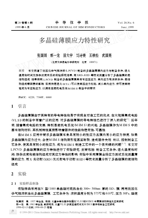
第20卷第6期 半 导 体 学 报 V o l.20,N o.6 1999年6月 CH I N ESE JOU RNAL O F SE M I CONDU CTOR S June,1999 多晶硅薄膜应力特性研究张国炳 郝一龙 田大宇 刘诗美 王铁松 武国英(北京大学微电子学研究所 北京 100871)摘要 本文报道了低压化学气相淀积(L PCVD)制备的多晶硅薄膜内应力与制备条件、退火,用XRD、R ED等技术测量分析了多晶硅膜的微结构组成.结果表明,L PCVD制备的多晶硅薄膜具有本征压应力,其内应力受淀积条件、微结构组成等因素的影响.采用快速退火(R TA)可以使其压应力松弛,减小其内应力,并可使其转变成为本征张应力,以满足在微机电系统(M E M S)制备中的要求.PACC:6220,7360F,68601 引言多晶硅薄膜由于其特有的导电特性和易于实现自对准工艺的优点,在大规模集成电路(VL S I)的制备中有着广泛的应用.对多晶硅薄膜的导电特性已进行了深入的研究[1].近年来,随着集成电路的发展,特别是微机电系统(M E M S)的兴起,多晶硅膜作为M E M S中的基本结构材料,其机械特性直接影响着器件的性能和稳定性、可靠性.在M E M S应用中要求多晶硅膜本身具有较小的张应力且膜内有小的应力梯度,如果多晶硅膜内应力过大,会使M E M S结构层形变甚至断裂,造成器件失效.所以,控制制备工艺条件,使其具有较小的张应力,成为M E M S制造工艺中的一个很关键的问题[2,3].本文对L PCVD多晶硅薄膜的应力特性进行了实验研究,主要包括:制备工艺条件、退火温度和时间、掺杂浓度和微结构组成对其应力特性的影响.实验中采用薄膜全场应力测试系统测量薄膜的应力,用X光衍射(XRD)及反射电子衍射(R ED)等技术测量分析了多晶硅膜的微结构组成.2 实验2.1 实验样品制备实验样品采用在N型(100)单晶硅衬底热生长300~500nm厚的Si O2膜;再用低压化学气相淀积生长多晶硅薄膜,工艺条件为:淀积温度分别为575℃和610℃,压力30Pa,硅烷张国炳 男,1937年出生,教授,从事半导体器件物理及VL S I和M E M S中薄膜结构特性及应用研究郝一龙 男,1963年出生,副研究员,从事VL S I多层互连技术及M E M S器件和制备工艺研究1998202213收到,1998208225定稿流量20scc m;淀积速率分别为313nm m in和615nm m in;膜厚2Λm和800nm;离子注入磷(P+)对多晶硅掺杂;为研究应力特性与退火温度的关系,我们采用快速退火(N2保护),退火温度从800~1100℃,退火时间30S,并在1100℃下改变退火时间(10~60秒).2.2 薄膜应力测量采用我所研制的薄膜全场应力测试仪测量多晶硅薄膜应力[4].用光偏振相移干涉原理,通过测量由于薄膜应力引起的衬底形变或曲率半径的变化,再转换成薄膜应力,其应力分布可表示为:Ρ(x,y)=Ρx+Ρy2=E T2S6(1-Μ)t F[52W(x,y)5x2+52W(x,y)5y2](1)其中 E和Μ为硅衬底的扬氏模量和泊松比;T S和t F分别为衬底和薄膜的厚度.该测量系统有下列优点:(1)应力测量具有全场性,可在整片上同时测量形变和应力分布;(2)测量精度高,可达10N c m2量级(形变量小于63nm);(3)测试范围为1×10²~1×10⁶N c m2.实验中,我们采取分别测量膜淀积前后、退火前后的基片形变,根据上式计算出膜的应力值. 2.3 多晶硅薄膜微结构组成的分析采用X光衍射技术(XRD)测量分析了多晶硅膜的相结构组成,仪器为日本理光DM A X22400型X光衍射仪(Cu)靶.测量衍射峰的半高宽(FW HM),根据Scherrer公式[5]可算出晶粒尺寸:D=kΚ Β(2Η)co sΗB(2)式中 K=0.9;Κ=0.15409nm;ΗB为B ragg角;Β(2Η)为经修正后的半高宽.3 实验结果和讨论3.1 淀积条件和离子注入掺杂对多晶硅膜本征应力的影响表1给出了不同淀积温度和不同离子注入掺杂浓度的多晶硅薄膜应力测量结果.表1 不同淀积温度和离子注入掺杂浓度对应力的影响编号1#2#3#4#5#24#25#淀积温度 ℃610610610610610575575注入掺杂能量 keV浓度 c m-21004×10141008×10141008×1015未注入未注入1002×1016未注入应力Ρ(×104N・c m-2)掺杂前-1.35-2.04-1.71-1.69-2.13-0.31-0.19掺杂后-1.45-2.10-2.06-1.69-2.03-0.75-0.19表1测量结果表明,575℃和610℃淀积的多晶硅薄膜,其应力为均压应力,但575℃淀积膜的应力明显低于610℃淀积膜的应力.离子注入掺杂在未退火前使多晶硅膜的压应力增加.3.2 退火温度对多晶硅薄膜本征应力的影响图1给出了不同淀积温度、不同掺杂浓度的多晶硅薄膜的本征应力随退火温度变化的测量结果.可以看出,多晶硅薄膜本征压应力随退火温度升高而减小,说明退火温度升高使多晶硅膜内应力松弛.在开始阶段,应力松弛的温度与掺杂浓度有关,未掺杂多晶硅膜的应464 半 导 体 学 报 20卷力松弛温度约为1000℃,而掺杂后使多晶硅膜的应力松弛温度降低.当退火温度大于1000℃时,570℃淀积的多晶硅薄膜应力可从压应力转变为张应力,而610℃条件下淀积的多晶硅薄膜则需较高的温度.图1 多晶硅膜本征应力与退火温度的关系图2 多晶硅薄膜本征应力与退火时间的关系3.3 退火时间对多晶硅薄膜应力的影响多晶硅薄膜本征应力与退火时间的关系如图2所示.其中,退火温度为1100℃.从图2可以看出,在1100℃下,多晶硅薄膜本征应力随退火时间增加而变小,t ≥20s 时,本征应力从压应力转变为张应力.5646期 张国炳等: 多晶硅薄膜应力特性研究 3.4 多晶硅薄膜微结构对本征应力的影响采用XRD 技术对不同的制备条件、不同退火条件的多晶硅膜的微结构进行了测量分析,结果表明,不同淀积条件和不同退火条件的多晶硅薄膜微结构有明显差异,这将对其内应力产生影响.图5 不同退火温度下多晶硅膜XRD 的谱(a )575℃下淀积、未掺杂;(b )575℃下淀积、掺杂;(c )610℃下淀积、掺杂.图3(见图版I )给出了575℃和610℃淀积的多晶硅薄膜XRD 谱.图3(a )为575℃下制备的样品,多晶硅膜具有较小的晶粒,平均尺寸D =16~17nm ,且取向较多:有(111),(220)(即(110)),(311)等晶向,其中(111)晶向的峰较强;同时,薄膜含有无定型的非晶成分.图3(b )为610℃下制备的多晶硅膜样品,晶粒尺寸较大,平均约为D =33nm ,晶粒生长具有明显的择优取向,即(110)方向,其他晶向的峰强度很小甚至消失,且不含有无定型成分.文献[5]中提到在不同温度下淀积多晶硅时,其微结构从非晶转变成多晶,转变温度在570℃左右.我们在575℃下淀积的薄膜包含有非晶和多晶的混合相,如图4(a )和(b )所示(见图版I ).这种结构的晶粒尺寸小、晶粒间界面积较大,取向中有较强的(111)方向,这种取向有明显的张应力增强作用[6],使膜的压应力变小,呈现出小压应力特性.610℃淀积的多晶硅膜晶粒较大(如图4(c ),(d )),有强的择优取向(110)方向,而(110)晶向将增强压应力[6],使薄膜有较大的压应力.离子注入掺杂在Si 中产生缺陷和损伤使压应力增大,随着退火温度增加,多晶硅膜微结构发生明显变化,使其晶粒长大即再结晶,如图4R ED 照片所示.从图5(a )、(b )中可以看出,经退火后衍射峰强度随退火温度升高而加强,并且晶粒尺寸增大,经1100℃30s 退火后,575℃下淀积的多晶硅膜掺杂样品的晶粒尺寸增至21nm ;610℃下淀积的薄膜的峰强度增加明显,未掺杂样品的晶粒尺寸4015nm ,而掺杂样品长大至46nm 左右,证明掺磷有促使晶粒长大的作用,这一点与文献报道一致[7].多晶硅微结构随退火温度的变化说明,经退火后多晶硅发生晶粒长大;其衍射峰强度增强表明发生再结晶后,择优晶向排列增强.再结晶是通过晶粒间界扩散使晶粒长大,晶粒间界面积变小,使体积收缩产生张应变[6],从而压应力松弛,即薄膜本征压应力减小甚至变成张应力.掺磷促进了再结晶过程,有利于压应力松弛,因此掺杂样品松弛温度稍低于未掺杂样品.664 半 导 体 学 报 20卷4 结论对L PCVD 多晶硅薄膜内应力与淀积条件和退火温度的关系进行了实验研究,结果表明575℃淀积的薄膜比610℃淀积的薄膜有较低的内应力.其内应力随退火温度增加及时间加长而减小,使压应力松弛,甚至可以变成张应力.多晶硅中掺磷有利于压应力松弛.XRD 、R ED 测量结果揭示了膜内应力的这些变化主要是由于薄膜微结构的改变引起的.575℃淀积的薄膜具有较小的晶粒尺寸,为非晶和多晶的混合结构,多种晶粒取向;610℃淀积的薄膜有较大的晶粒尺寸和明显优选的晶向.采用R TA 退火具有时间短,热积累少,对器件性能影响小的优点,可作为在M E M S 制备中控制多晶硅内应力的一种有效方法.参考文献[1] T .I .Kam ins ,J .E lectrochem .Soc .,1980,127:686.[2] M .M eh regang ,IEEE T rans .,E lectron D evices ,1988,35:719.[3] KuehnelW .,Senso r &A ctuato rs ,1994,A 45:7~16.[4] Guoying W u ,Guobing Zhang ,Yilong H ao ,P roc .of 11th IEEE VM I C ,Santa C lara ,U SA ,1994,221~229.[5] G .H arbeke ,J .E lectrochem .Soc .,1984,131:675.[6] J .H uang ,P .K rulevich ,M at .R es .Soc .P roc .,1990,182:201.[7] Yasuo W ada ,J .E lectrochem .Soc .,1978,125:1499.Residua l Stress Properties of Polysil icon Th i n F il mZhang Guob ing ,H ao Y ilong ,T ian D ayu ,L iu Sh i m ei ,W ang T iesong ,W u Guoying(Institu te of M icroelectronics ,P ek ing U niversity ,B iej ing 100871)R eceived 13February 1998,revised m anuscri p t received 25A ugust 1998Abstract T h is p ap er has investigated the effets of p rocess conditi on ,annealing tem p era 2tu re ,annealing ti m e and dopp ed concen trati on on the residual stress of L ow P ressu re Chem ical V apo r D epo siti on (L PCVD )Po lysilicon th in fil m .T he m icro structu re of the fil m is studied by X 2ray diffracti on (XRD )and reflecti on electron diffracti on (R ED ).T he re 2su lts show that the in ital com p ressive stress is relaxed w ith annealing tem p retu re and ti m e by rap id therm al annealing (R TA ).H igh tem p reatu re of annealing (R TA )can change the state of the residual stress from com p ressi on to ten si on .T he low ten sile stress is su itab le fo r M icroelectrom echan ical System (M E M S ).PACC :6220,7360F ,68607646期 张国炳等: 多晶硅薄膜应力特性研究 。
带隙基准

Key words: Bandgap Reference; Layout; Power Supply Rejection Ratio; Temperature Coefficient
III
目
第1章 1.1
录
绪论············································································ 1 带隙基准源概述······························································1 1.1.1 1.1.2 带隙基准源的研究现状········································· 1 研究目的及意义···········································设计········································· 17 3.2.1 3.2.2 3.2.3 3.2.4 3.2.5 设计指标·························································· 17 带隙基准源架构·················································17 核心电路设计···················································· 20 运放设计·························································· 22 偏置电路设计···················································· 23
重掺_100_硅单晶抛光片条纹状起伏缺陷研究

重掺<100>硅单晶抛光片条纹状起伏缺陷研究王云彪,张为才,武永超,陈亚楠(中国电子科技集团公司第四十六研究所,天津 300220)摘 要:重掺<100>硅单晶片抛光后经微分干涉显微镜观测,抛光片边缘区域存在条纹状起伏缺陷。
通过分析条纹状起伏缺陷与重掺硅单晶中杂质的分布状况和<100>晶面本身腐蚀特性的关系,阐述了条纹状起伏缺陷形成的机理。
通过工艺试验,对比了不同工艺条件下抛光片表面微观形貌状况,分析了抛光过程中各工艺条件对表面条纹起伏缺陷的影响,采用3步抛光工艺,得到了表面平整和一致性好的抛光片表面,抛光片边缘无条纹起伏缺陷。
关键词:条纹起伏缺陷;微观形貌;抛光片中图分类号:TN305 文献标识码:A 文章编号:1001-3474(2012)05-0312-04Research of Striped Rolling Defects on Heavily Doped <100> Polished Silicon WafersWANG Yun-biao, ZHANG Wei-cai, WU Yong-chao, CHEN Ya-nan(No.46 Research Institute of CETC, Tianjin 300220, China)Abstract: Using differential interference contrast microscope observed striped rolling defects on the edge regions of Heavily doped < 100 > polished silicon wafers. Expounded the formation mechanism of the stripe rolling defects by analyzing the relationship between stripe rolling defects and the impurities distribution in heavily doped silicon crystal and the surface corrosion characteristics of <100> crystal orientation. Compared the surface microtopography with different polishing process conditions, researched the influence of polishing process conditions on surface striped rolling defects. Got polished silicon wafers with highly smooth surface, good consistency and no edge stripe rolling defects using three steps polishing process,.Keywords: Stripe rolling defects; Microtopography; Polished wafers Document Code: A Article ID: 1001-3474(2012)05-0312-04随着半导体工艺技术的不断进步,微机械与微电子电路对硅单晶衬底片的要求越来越高[1,2]。
硅基马赫曾德电光调制设计优化与实现

硅基马赫曾德电光调制设计优化与实现周林杰;周砚扬;陆梁军【摘要】In this paper,the design optimization and experimental demonstration of single-drive push-pull silicon electro-optic modulators are presented. In order to improve the modulation efficiency and lower the optical propagation loss,the PN junction profile and doping concentrations are firstly optimized. Next,the impedance match,phase match and microwave loss are studied,and in particular,the influence of low-doping slab width,travelling-wave electrode (TWE) width and spacing on the modulator performance are analyzed. Following the comprehensive theoretical analysis and numerical simulation,the modulator performance measurements,including the optical transmission spectrum upon single-drive push-pull tuning,small-signal microwave signal response,and high-speed digital signal modulation are consequently carried out. The on-chip insertion loss of the modulators is around 7-9 dB and the half-wave voltage is 5 V. At a bias voltage of 0 V,the optimized modulator has a modulation bandwidth of >18 GHz. The microwave reflectivity at the entrance of the TWE is less than -20 dB,suggesting good impedance match. When the reverse bias voltage is increased to 4 V,the modulation bandwidth can exceed 30 GHz,allowing for realization of 56 Gbit/s on-off keying (OOK) and 40 Gbit/s binary phase-shift keying (BPSK) modulations.%对单端推挽驱动硅基调制器进行了优化设计和实验验证.为了获得较高的调制器性能,首先对PN结的结构参数和掺杂浓度进行了仿真优化,以提高调制效率并降低光传输损耗;其次,对行波电极的阻抗匹配、相位匹配和微波损耗予以了研究,重点分析了低掺杂平板区宽度、行波电极传输线宽度(TWE)和间距对调制性能的影响.在理论分析和仿真计算的基础上,对单端推挽驱动调制器进行了频谱测试、小信号响应测试和高速调制码型测试.调制器的片上插入损耗在7~9 dB,半波电压约为5 V.偏置电压为0 V时,优化后的调制器的带宽大于18 GHz,入射端反射系数低于-20 dB,行波电极具有较好的阻抗匹配.当反偏电压大于4 V时,调制器的带宽可增加到30 GHz以上,并且能实现56 Gbit/s的二进制强度(OOK)调制和40 Gbit/s的二进制相移键控(BPSK)调制.【期刊名称】《中兴通讯技术》【年(卷),期】2017(023)005【总页数】9页(P21-29)【关键词】电光调制器;硅基光电子;高速收发模块;光电子器件【作者】周林杰;周砚扬;陆梁军【作者单位】上海交通大学,上海200240;上海交通大学,上海200240;上海交通大学,上海200240【正文语种】中文【中图分类】TN929.5硅基电光调制器由于其综合性能出众,吸引了全球各高校、研究所和企业的持续关注。
基于Taguchi-GA协同的磁性磨料抛光性能预测及制备工艺参数寻优
第51 卷第 4 期2024年4 月Vol.51,No.4Apr. 2024湖南大学学报(自然科学版)Journal of Hunan University(Natural Sciences)基于Taguchi-GA协同的磁性磨料抛光性能预测及制备工艺参数寻优王燎原1,孙玉利1†,张桂冠2,吴鹏飞1,易思广1,孙业斌1,左敦稳1(1.南京航空航天大学机电学院,江苏南京 210016;2.山东理工大学先进制造研究院,山东淄博 255049)摘要:通过改变黏结法磁性磨料的制备工艺参数来设计正交试验,制备不同系列规格的磁性磨料,并对其进行形貌和成分检测.以3D打印AlSi10Mg板为加工对象,通过平面磁力研磨试验,揭示磁性磨料制备工艺参数对磁力研磨质量的影响规律.基于回归分析,建立参数与响应之间的回归模型,通过遗传算法实现参数优化. 结果表明,在SiC粒径为18~25 µm,Fe与SiC的质量比为4.7,环氧树脂与聚酰胺的质量比为2,固化温度为100 ℃的条件下,材料去除率为1.7 mg/min,表面粗糙度由原始的3.90 µm降低至0.27 µm,降低率为93.1%.关键词:优化;遗传算法;磁性磨料;磁力研磨;抛光性能中图分类号:TH16;TB333 文献标志码:APredicting Polishing Performance of Magnetic Abrasive and Optimizing ItsPreparation Process Parameters Based on Taguchi-GA SynergyWANG Liaoyuan1,SUN Yuli1†,ZHANG Guiguan2,WU Pengfei1,YI Siguang1,SUN Yebin1,ZUO Dunwen1(1.College of Mechanical and Electrical Engineering, Nanjing University of Aeronautics and Astronautics, Nanjing 210016, China;2.Institute for Advanced Manufacturing, Shandong University of Technology, Zibo 255049, China)Abstract:In this study,an orthogonal experiment was designed by changing the preparation process parameters of bonded magnetic abrasives. Then,a series of magnetic abrasives with different specifications were prepared,and their morphology and composition were detected. Taking the 3D-printed AlSi10Mg plate as the processing object, the influence of the magnetic abrasive preparation process parameters on the polishing quality was revealed through the planar magnetic abrasive finishing experiment. A regression model between parameters and responses was established based on regression analysis, and the genetic algorithm optimized parameters. The results show that under the condition that SiC is 18~25 µm, the mass ratio of Fe to SiC is 4.7, the mass ratio of resin to∗收稿日期:2023-10-14基金项目:南京航空航天大学博士研究生拔尖创新人才培养“引航计划”跨学科创新基金项目(KXKCXJJ202307),Interdisciplinary Inno⁃vation Fund for Doctoral Students of Nanjing University of Aeronautics and Astronautics (KXKCXJJ202307);南京航空航天大学研究生创新实验竞赛培育项目,Graduate Innovative Experiment Competition Cultivation Project Fund of Nanjing University of Aeronautics and Astronau⁃tics;南京航空航天大学博士学位论文创新与创优基金项目(BCXJ22-08),Nanjing University of Aeronautics and Astronautics Doctoral Disser⁃tation Innovation and Excellence Fund (BCXJ22-08)作者简介:王燎原(1992―),男,河南新乡人,南京航空航天大学博士研究生† 通信联系人,E-mail:****************.cn文章编号:1674-2974(2024)04-0043-11DOI:10.16339/ki.hdxbzkb.2024169湖南大学学报(自然科学版)2024 年curing agent is 2,the curing temperature is 100 °C,the material removal rate is 1.7 mg/min,and the surface roughness is reduced from the original3.90 µm to0.27 µm with a reduction of 93.1%.Key words:optimization;genetic algorithm;magnetic abrasive;magnetic abrasive finishing;polishing performance磁力研磨是一种非传统的抛光技术,可通过变化的磁场力来驱动导磁性磨料,进而实现对工件的光整加工[1-2]. 作为加工工具,磁性磨料无疑是决定磁力研磨性能的关键[3]. 磁性磨料主要由铁基体、硬质磨料、结合剂或增稠剂组成. 目前,磁性磨料的制备工艺主要有烧结法[4]、机械合金化法[5]、雾化快凝法[6]、黏结法[7]及简单混合法[8]等,其制备工艺参数对磁性磨料的品质起着决定性作用,也逐渐成为国内外学者研究的焦点. Chen等[9]对烧结法磁性磨料的表面形貌和成分进行了表征,研究了烧结时间及烧结温度对磁性磨料性能的影响,进而优化了磁性磨料的烧结工艺. Gao等[10]通过理论建模揭示了雾化快凝磁性磨料中铁磁体含量及磁性磨料粒径等参数对材料去除率的影响规律. Singh等[11]研究了退火温度对机械合金化磁性磨料的导磁及加工性能的影响,揭示了磁性磨料的微切削机理. Li等[12]通过理论结合实验的方法,探究了铁磁相与磨粒相的粒径比及质量比对磁性磨料抛光性能的影响,为黏结磁性磨料的制备提供了理论依据. Heng等[13]创新性地将碳纳米管和铁颗粒混合到金刚石研磨膏中,通过机械混合制得磁性磨料,有效解决了ZrO2陶瓷材料的难抛光问题.研究表明,黏结法相比于烧结法、机械合金化法及雾化快凝法,具有工艺简单、成本低、制备周期短等优点[14]. 同时,相比简单混合法磁性磨料,黏结法磁性磨料又展现出结合力强、加工效率高、服役寿命长等优点[15]. 因此,黏结法磁性磨料有望成为应用最广泛的加工工具. 大多数公开文献直接以黏结法磁性磨料作为工具,对磁极转速、磁场强度、加工间隙等加工参数进行深入研究[16-17]. 然而,由于技术封锁和专利保护等原因,很少有公开文献对黏结法磁性磨料最关键的制备工艺参数进行详尽地剖析和优化,一定程度限制了磁力研磨技术的推广.本文通过调节黏结法磁性磨料的4个关键参数,即磨粒相的粒径、Fe与SiC含量、黏结剂配比、固化温度,制备系列不同形貌和物理性能的磁性磨料.基于正交试验法,采用平面磁力研磨对3D打印AlSi10Mg板进行抛光. 以材料去除量Δm和表面粗糙度降低率ΔR a为指标,揭示了工艺参数与抛光性能之间的内在关系,建立其数学模型,并通过遗传算法(Genetic Algorithms,GA)进行参数优化. 本文工作有望为黏结法磁性磨料的工艺优化提供有价值的研究思路.1 磁性磨料的制备黏结法磁性磨料的制备工艺流程如图1所示,具体步骤如下:将环氧树脂和聚酰胺按一定比例混合作为胶黏剂,并加入40 mL丙酮进行稀释. 向胶黏剂中加入质量分数为5%且表面用KH550改性过的纳米填料KH-Al2O3,以改善树脂固化物的力学性能[18].对黏结剂溶液超声分散5 min并磁力搅拌均匀.将黏结剂、Fe、SiC一同加入300 mL无水乙醇中,并搅拌均匀.然后,在水浴环境下对混合物持续搅拌以促使乙醇挥发,并获得黏稠状的混合物.利用模具将黏稠状混合物压制成坯,并将坯体在恒温箱中加热固化.之后,进行破碎、筛分以获得粒径为375~750 µm的磁性磨料. 所用的粉体和胶黏剂的质量比为16∶3,Fe粒径为18~25 µm.图2为本文所制备磁性磨料的形貌及成分表征. 该磨料的制备参数为:SiC平均粒径为30 µm,Fe图1 黏结法磁性磨料的制备工艺流程Fig.1 Process flow for the preparation of bondedmagnetic abrasives44第 4 期王燎原等:基于Taguchi-GA 协同的磁性磨料抛光性能预测及其制备工艺参数寻优与SiC 的质量比为4∶1,环氧树脂和聚酰胺的质量比为5∶3,固化温度为90 ℃. 由图2可知,该磁性磨料整体上呈不规则状. Fe 和SiC 颗粒在基体中均匀分布. 对图2(b )中A 和B 两个区域进行EDS 检测,结果分别如图2(c )和图2(d )所示. 分析可知,磁性磨料主要含C 、O 、Al 、Si 及Fe 元素. 其中,C 元素主要来自树脂及SiC ,O 元素主要来自树脂,Si 元素主要来自SiC 磨料,Al 元素主要来自纳米Al 2O 3. A 处Si 谱峰最强且含量最高,B 处Fe 谱峰最强且含量最高,证实了两处分别为SiC 和Fe.2 试 验2.1 加工原理图3为磁力研磨试验原理图.将7个轴向充磁、牌号为N30的圆柱形磁铁嵌入磁极头中,中心磁极为N 极朝外,圆周均布的6个磁极为S 极朝外.磁性磨料沿着磁力线的方向排布以形成磁力刷并压覆于工件表面.磁极高速旋转提供主加工运动,工件的往复运动实现横向进给.2.2 方 法工件是3D 打印的AlSi10Mg 薄板,尺寸为65 mm×45 mm×2 mm.在试验前,其表面经过喷砂处理,表面粗糙度为4 µm.每个工件抛光40 min ,每间隔10 min 更新一次磨料,以保证加工的一致性. 利用精密天平(Mettler Toledo , 精度0.000 1 g )测量工件加工前、后的质量,并计算差值Δm ,用以表征材料去除效率;用针触式粗糙度测量仪(Mitutoyo )检测工件表面粗糙度R a ,在工件的加工区域均匀选取5个点记录表面粗糙度值并取其平均值作为该试件的R a 值.用表面粗糙度降低率ΔR a 来表征抛光质量,其计算公式如下:ΔR a =R a0-R a1R a0(1)(a )放大140倍(b )放大1 000倍(c )A处的能谱图(d )B 处的能谱图图2 磁性磨料的形貌及成分表征Fig.2 Morphology and compositional characterization of themagnetic abrasive图3 磁力研磨试验原理图Fig.3 Schematic diagram of magnetic abrasive finishing45湖南大学学报(自然科学版)2024 年式中: R a0、R a1分别为加工前、后的表面粗糙度.用扫描电子显微镜(SEM, Quanta FEG 250)观察磁性磨料形貌;利用振动样品磁强计(VSM, LakeShore 7404)检测磁性磨料的磁滞回线;利用激光共聚焦显微镜(UP-lambda,艾泰克仪器科技有限公司)观测工件表面的三维形貌. 磁力研磨工艺参数如表1所示.2.3 磨料参数本文主要研究磁性磨料的制备工艺参数和其抛光性能之间的对应关系. 以SiC的粒径A:d mesh,单位为μm;B: Fe与SiC的质量比φpowder;C:环氧树脂和聚酰胺的质量比δadhesive;D:固化温度T(单位为℃)为自变量. 以材料去除量Δm和表面粗糙度降低率ΔR a为研究指标,选用L16(45)正交试验表开展试验. 因素与水平如表2所示,正交试验结果如表3所示.在极差分析、方差分析、回归方程建模中,采用磨粒粒径范围的上限所对应的筛网目数作为相应的因素水平.3 结果与讨论3.1 极差分析利用Minitab软件对试验数据进行分析,其极差分析结果如表4所示.由表4可知,磁性磨料参数对Δm的影响程度的顺序为:D>A>B>C. 当固化温度为90 ℃,SiC的粒径为25~30 µm,Fe与SiC的质量比为4∶1,环氧树脂和聚酰胺的质量比为5∶2时,Δm可达到最大值.磁性磨料参数对ΔR a的影响程度的顺序为:D>B>A>C. 当固化温度为90 ℃,Fe与SiC的质量比为4∶1,SiC的粒径为25~30 µm,环氧树脂和聚酰胺的质量比为5∶3时,ΔR a可达到最大值.图4为Δm和ΔR a的均值响应曲线. 由图4可知,随着SiC粒径的增加,Δm和ΔR a先增加后减少,且极大值均在25~30 µm处取得.研究表明,磨料粒径越小,材料去除率越低[19].由于原始工件的R a较高,在相同的时间,小粒径SiC不能有效地改善工件表面的微观不平度.但磨料粒径过大,将会使磁性磨料的微切削性能下降. 图5为SiC粒径为75~150 µm的磁性表1 磁力研磨工艺参数Tab.1 Process parameters of magnetic abrasive finishing参数磁铁尺寸/(mm×mm)磁极速度/(r·min-1)加工间隙/mm进给速度/(mm·s-1)磁性磨料用量/g润滑油用量/mL值ϕ8×151 500253.52.5表3 正交试验结果Tab.3 Orthogonal experimental results标号12345678910111213141516因素A7~127~127~127~1210~1310~1310~1310~1325~3025~3025~3025~3075~15075~15075~15075~150B4821482148214821C2.501.671.251.001.672.51.001.251.251.002.501.671.001.251.672.50D306090120901203060120906030603012090误差1234432121433412Δm/mg26.526.339.422.063.547.523.028.458.545.564.827.436.912.757.045.5ΔR a/%70.2575.3778.6468.7589.8480.6566.3072.5088.7079.3186.4470.1275.9663.7583.5977.05表2 因素与水平表Tab.2 Factors and levels水平1 2 3 4因素A7~1210~1325~3075~150B4821C2.50 (5∶2)1.67 (5∶3)1.25 (5∶4)1.00 (5∶5)D306090120表4 极差分析结果Tab.4 Results of range analysis指标Δm/mgΔR a/%水平K1K2K3K4极差最优方案K1K2K3K4极差最优方案因素A114.2162.4196.2152.182.0D3A3B1C1293.01309.28324.56300.3631.55D3B1A3C2B185.4132.0184.2123.362.1324.75299.08314.97288.4236.33C184.3174.2139.0127.456.9314.39318.92303.59290.3228.60D89.6156.4193.9185.0104.3270.42310.27324.84321.6954.4246第 4 期王燎原等:基于Taguchi-GA 协同的磁性磨料抛光性能预测及其制备工艺参数寻优磨料形貌、成分及及其失效图解.图5(a )显示该磁性磨料表面嵌有数个较大的块状物. 对图5(b )中方框所在区域B 进行放大,并对B 区域进行元素检测,结果如图5(c )所示. 分析可知,该区域内C 元素和Si 元素含量极高,根据SiC 的原子质量关系可确认块状物为SiC. 由图5(d )可知,由于SiC 的粒径较大,在相同的含量下,磁性磨料所能容纳的SiC 颗粒数较少. 在加工过程中,由于SiC 频繁承受剪切力,而使得强度相对较低的基体优先发生微断裂. 最终,含有SiC 的大块碎片从磁性磨料上脱落,进而影响磁性磨料后续的切削性能.在研磨压力和切削速度一定时,仅通过增大磨料的粒径并不能有效提高材料去除率.包含了大量小粒径SiC 的磁性磨料可使SiC 在抛光中逐步脱落,既避免了切削性能的骤降,又保证了材料去除率.磁性磨料的导磁性能主要通过改变Fe 与SiC 的质量比φpowder 来进行调控.由图4可知,随着φpowder 的增加,Δm 和ΔR a 都出现了先增加后下降的趋势.该现象可由图6所示的磁性磨料的磁滞回线来解释. 随着Fe 含量的增加,磁性磨料的磁化率和磁饱和强度增加.当φpowder 为1时,磁性磨料的导磁性最差. 此时在磁极高速旋转下,大量的磁性磨料将挣脱磁场力的约束而飞出加工区域,导致抛光质量下降.当φpowder 为8时,SiC 含量较少,导致磁性磨料的切削性(a )放大100倍(b )放大300倍(c )EDS能谱图(d )磁性磨料失效机理图5 SiC 粒径为 75~150 µm 的磁性磨料形貌、成分及其失效图解Fig.5 Morphology , composition and failure analysis of magneticabrasive containing the SiC with a diameter of 75~150 µm(a )Δm均值响应曲线(b )ΔR a 均值响应曲线图4 Δm 和ΔR a 的均值响应曲线Fig.4 Mean response curves of Δm and ΔR a47湖南大学学报(自然科学版)2024 年能不足.分析可知,Fe含量越高,磁性磨料导磁性能越强,但磁性磨料导磁性能的增强是以牺牲其切削性能为代价而实现的. 因此,存在折中的Fe含量,使两均值曲线出现极值点.由图4可知,随着δadhesive的增大,Δm增加,但ΔR a 先增加后减少. 该现象主要与树脂基体的力学性能密切相关. δadhesive为1.00时磁性磨料的形貌图如图7所示. 磁性磨料表面呈现出钝化和塑性变形的区域,而SiC的出露高度较小. Wang等[20]研究表明,聚酰胺兼具固化和增韧环氧树脂的作用. 聚酰胺分子中含有较长的柔性亚甲基链结构,聚酰胺含量越高,环氧树脂固化物的冲击韧性越高,但刚性越低[21]. 在破碎大块磁性磨料的过程中,破碎叶片的高速冲击使得基体以塑性变形来抵消冲击能[18],致使SiC被包覆于基体中. 同理,在抛光时SiC磨料也会向软的基体内部退让,致使磁性磨料的抛光能力减弱.随着δadhesive的增加,环氧树脂固化物刚性和硬度增加,但其宏观脆性也显著增大[22]. 当δadhesive为2.50时,磁性磨料在频繁滑擦工件表面后,基体发生脆性微断裂,漏出新的切削刃,对材料去除有一定的促进作用,Δm仍然呈现增大趋势. 但在加工到特定时间后,新的切削刃将会对已加工好的表面进行二次损伤,限制ΔR a的进一步提升. δadhesive为2.50时磁性磨料抛光后的工件表面形貌如图8所示,由图8可知,表面存在多条较深的划痕,整体表面质量下降,这也验证了上述分析结果.固化温度T主要影响环氧树脂的固化反应过程. 随着T的增加,环氧树脂的固化反应加快,其固化物的力学性能如硬度及刚性等可得到提高[23]. 当T为30 ℃时,Δm和ΔR a均处于较低的水平,这是因为此条件下的树脂结合剂不能充分固化,导致磁性磨料的结合强度较低. 当固化温度为30 ℃时,磁性磨料的形貌图如图9所示. 由图9可知,大部分磁性磨料呈现松散状,表明黏结剂对各组分的把持力不足,不能满足高效、高质量抛光要求.在一定范围内,随着T的增加,Δm和ΔR a均增加. 但当T提高到120 ℃时,树脂固化物发生变性,出现不同程度的软化和热变形的现象[24]. 当固化温度为120 ℃时,磁性磨料形貌如图10所示. 由图10可知,磁性磨料在破碎时,部分区域被破碎叶片削平,呈现软塑状态,证实了该条件下基体发生了软化,磁性磨料的抛光性能也随之下降.3.2 方差分析为了进一步精确估计因素及误差的显著性,验证极差分析法的合理性,对响应数据进行方差分析,其结果如表5所示.分析可知,所选的四个因素对Δm和ΔR a两个指标均有显著的影响,而误差的影响极小,证明了正交试验设计的合理性.根据F值的大图8 δadhesive为2.50时磁性磨料抛光后的工件表面形貌Fig.8 The surface morphology of workpiece after magneticabrasive finishing with δadhesiveof 2.50图7 δadhesive为1.00时磁性磨料的形貌图Fig.7 The morphology of magnetic abrasive whenδadhesiveof 1.00图6 磁性磨料的磁滞回线Fig.6 Hysteresis loop of magnetic abrasives48第 4 期王燎原等:基于Taguchi-GA 协同的磁性磨料抛光性能预测及其制备工艺参数寻优小,因素对Δm 和ΔR a 的影响程度的顺序分别为: D>A>B>C ,D>B>A>C ,方差分析结果与极差分析结果相吻合.3.3 回归方程为了消除数据之间的量纲和取值范围差异的影响,提高回归模型的预测精度,对样本数据进行归一化处理. 本文基于sk-learn 框架,采用min-max 归一化处理技术,将自变量的数据集成员映射到[0,1][25].其理论计算如下[26]:x new =x origin -x minx max -x min(2)式中:x new 、x origin 、x min 、x max 分别为归一化的数据、原始数据、原始数据中的最小值和最大值.利用Minitab 软件对归一化的正交试验数据进行回归分析,分别建立关于Δm 和ΔR a 的多元回归方程,结果如式(3)和式(4)所示. 两方程的校正R 平方分别为0.92和0.96,预示着回归模型对数据集具有良好的拟合效果.Δm =11.04+38.3a +62.7b +14.41c +66.9d - 49.8a 2-63.6b 2-42.6d 2(3)ΔR a =58.82+18.93a +35.36b +23.99c +36.82d -21.95a 2-33.63b 2-17.9c 2-24.19d 2(4)式中:a 、b 、c 、d 分别为归一化的自变量数据.3.4 遗传算法寻优遗传算法(GA )是受到遗传机制和自然选择的启发而衍生出的一种元启发式随机全局寻优算法. GA 将被优化的参数进行编码,组成一条染色体,其表5 方差分析结果Tab.5 Analysis of variance results指标Δm /mgΔR a /%来源A B CD误差总计A B CD误差总计自由度33333153333315调整离差平方和854.81826.17559.721 671.5820.273 932.56138.44196.59121.60470.681.92929.22调整均方284.94275.39186.57557.196.7646.1565.5340.53156.890.64F 值42.1740.7527.6182.4672.18102.5063.40245.40显著性***************注:*为显著;**为非常显著.(a )放大30倍(b )A 区域放大140倍图9 当固化温度为30 ℃时,磁性磨料的形貌图Fig.9 The morphology of magnetic abrasive at a curingtemperature of 30 ℃(a )放大100倍(b )放大500倍图10 当固化温度为120 ℃时,磁性磨料的形貌图Fig.10 The morphology of magnetic abrasive at a curingtemperature of 120 ℃49湖南大学学报(自然科学版)2024 年中每一个参数代表一个基因,每一个解对应一条染色体. 类比生物进化论的思想,以适应度函数作为评价优劣的标准,经过选择、交叉、变异后,淘汰劣势个体,保留适应能力强的遗传信息,并遗传给下一代. 在多代寻优后即可挑选出最优的个体,即问题的最优解[27-28]. 如图11所示,本文GA 的运行流程主要包括种群初始化、适应度值计算、基因操作(选择、交叉和变异)、迭代终止判断等模块,并通过Python 中的PyGAD 框架实现编程和迭代计算,具体操作如下:1)初始化. 综合考虑问题的复杂程度、算法收敛速度、种群多样性,随机生成10条染色体,即初始生成10组解. 每条染色体包含4段基因,分别对应4个待优化的参数. 基因值分别在归一化的搜索空间 [0,1]内随机取得.2)适应度. 适应度值是用来衡量解的优异性的重要指标,通常由特定的适应度函数F (X )求得. 本文的适应度函数是来源于正交试验中的多元回归方程,表达式如式(5)所示.F (X )=α f 1(X )+β f 2(X )(5)式中:f 1和f 2分别代表关于Δm 和ΔR a 的多元回归方程;X 为某一自变量组合;α和β分别代表权重系数.当α=1且β=0时,F (X )可代表关于Δm 的适应度函数;反之F (X )为关于ΔR a 的适应度函数.3)选择. 基于优胜劣汰的生存法则,将适应度较高的个体挑出来进行交配,以产生后代. 本文基于轮盘赌选择法(Roulette Wheel Selection , RWS )原理进行选择操作. 在RWS 中,将圆轮划分为n 份,代表种群中的n 个个体. 其中,每一份所占的面积正比于个体的适应度值. 在轮子的圆周方向固定一个指针,当圆轮停止旋转后,被选中的个体可将遗传信息遗传至后代[29]. 因此,适应度大的个体被选中的概率大. 在每一代的种群中,将有2个个体被选中.4)交叉. 交叉操作类似于遗传学中的基因重组技术,是GA 生成后代个体的关键. 本文将采用常见的单点交叉(Single Point Crossover ,SPC )技术. 在一对父母的染色体上随机选取一个截断点,截断点之后的基因序列将发生互换,以此来产生新的后代,发生基因互换的概率设为0.8 [30].5)变异. 变异操作类似于遗传学中的基因突变,可以保证后代基因的多样性,通常以小概率发生. 本文采用随机重置(Random Resetting , RR )方法,可从变量的搜索空间中随机选择一个后补的基因值替换掉对应位置的基因值,变异发生的概率设为0.01[31].6)终止循环. 当迭代次数超过500个周期即可终止循环.3.5 优化结果图12为适应度与迭代次数的关系曲线. 由图12可知,随着迭代次数的增加,适应度曲线增加到某数值后趋于稳定,预示着在500个周期内GA 可达到收敛.表6为实验和GA 寻优的结果对比,其中,因素A 用筛网的目数表示. 方案1和方案3数据分别为关于Δm 及ΔR a 的正交试验优选方案. 在此条件下,实验值和预测值之间的误差分别为3.8%和1.3%,证明了回归模型具有良好的预测功能. 本文中SiC粒径的图11 GA 算法流程图Fig.11 GA flowchart图12 适应度与迭代次数的关系曲线Fig.12 Curves of the relationship between fitness anditeration count50第 4 期王燎原等:基于Taguchi-GA协同的磁性磨料抛光性能预测及其制备工艺参数寻优第3水平位于25~30 µm之间,GA优化的值在此区间之外. 综合考虑国标粒径、筛分难度和工程精度要求,均选用粒径为18~25 µm的SiC作为两响应的最优参数. 同理,将其余参数也进行圆整化,结果如表6中圆整-GA行所示. 针对Δm和ΔR a,圆整-GA寻优误差分别为1.8%和2.7%,表明GA算法具有良好的寻优效果.根据工程实践,在粗加工时往往通过加大材料去除率来实现表面平整度的快速提升. 但在精加工阶段,则需要通过材料的微去除来进一步修饰和提升表面质量. 因此,在本试验中可认为ΔR a相较Δm 具有更高的重要性和优先性. 优选方案对比图如图13所示,由图13可知,方案4最终可实现93.1%的表面粗糙度降低率,同时也能保证一定的材料去除率.因此,最优方案为:SiC粒径为18~25 µm,Fe与SiC的质量比为4.7,环氧树脂与聚酰胺的质量比为2,固化温度为100 ℃,材料去除率为1.7 mg/min.图14为最优方案的抛光效果图.未抛光的原始区域A比较粗糙且存在明显的凹坑,而抛光后的B 区域出现了清晰的校徽倒影,原始工件的表面三维形貌得到了有效的提高. 经过抛光后,表面粗糙度由原始的3.90 µm降低到0.27 µm,验证了该磁性磨料具有优异的抛光性能.表6 实验和GA寻优的结果对比Tab.6 Comparison between experimental results and optimization results of GA优化指标Δm/mg ΔR a/%方案1234方法TaguchiGA圆整-GATaguchiGA圆整-GA因素A500638.16600~800500708.31600~800B44.494.544.684.7C2.52.482.51.672.012D90100.871009099.24100实验值70.573.291.293.1预测值73.1874.5392.3594.24误差/%3.81.81.32.7图13 优选方案对比图Fig.13 Comparison of different optimal solutions(a)实物图(b)A区域原始形貌(c)B区域抛光后形貌图14 最优方案的抛光效果图Fig.14 The polished effect image using the best solution51湖南大学学报(自然科学版)2024 年4 结论本文基于Taguchi-GA法对黏结法磁性磨料的制备工艺进行探究并实现了参数优化,所获得的结果如下:1)基于正交试验建立了Δm和ΔR a关于SiC粒径、Fe与SiC质量比、环氧树脂与聚酰胺质量比及固化温度的函数表达式,进而采用遗传算法实现参数优化,最终通过实验验证了模型的合理性.2)SiC粒径显著影响磁性磨料的微切削性能. 随着SiC目数的增加,Δm和ΔR a先增加后下降;Fe的含量主要影响磁性磨料的导磁性能. 随着Fe与SiC的质量比的增加,Δm和ΔR a先增加后下降.3)在一定范围内增加环氧树脂与聚酰胺质量比可提高磁性磨料基体的硬度和刚度,进而提高磁性磨料的抛光性能;在基体的耐热温度范围内,提高固化温度可显著提高磁性磨料的抛光性能.4)在SiC粒径为18~25 µm,Fe与SiC的质量比为4.7,环氧树脂与聚酰胺的质量比为2,固化温度为100 ℃的条件下,材料去除率为1.7 mg/min,表面粗糙度由原始的3.90 µm降低至0.27 µm,降低率为93.1%.5)本研究成果可为黏结法磁性磨料的优化提供技术参考,有望推动磁性磨料的广泛工程应用.参考文献[1]WU J Z,ZOU Y H,SUGIYAMA H.Study on finishing characteristics of magnetic abrasive finishing process using low-frequency alternating magnetic field[J].The InternationalJournal of Advanced Manufacturing Technology,2016,85(1):585-594.[2]GUO J,LIU K,WANG Z F,et al.Magnetic field-assisted finishing of a mold insert with curved microstructures for injectionmolding of microfluidic chips[J].Tribology International,2017,114: 306-314.[3]WANG L Y,SUN Y L,CHEN F Y,et al.Experimental study on vibration-assisted magnetic abrasive finishing for internal blindcavity by bias external rotating magnetic pole[J].PrecisionEngineering,2022,74: 69-79.[4]AHMAD S,GANGWAR S,YADAV P C,et al.Optimization of process parameters affecting surface roughness in magneticabrasive finishing process[J].Materials and ManufacturingProcesses,2017, 32(15): 1723-1729.[5]SINGH P,SINGH L,SINGH S.Manufacturing and performanceanalysis of mechanically alloyed magnetic abrasives for magnetoabrasive flow finishing[J].Journal of Manufacturing Processes,2020,50:161-169.[6]GAO Y W,ZHAO Y G,ZHANG G X,et al.Characteristics of a novel atomized spherical magnetic abrasive powder[J].TheInternational Journal of Advanced Manufacturing Technology,2020,110(1):283-290.[7]AHN B W,LEE S H.Run-to-run process control of magnetic abrasive finishing using bonded abrasive particles[J].Proceedings of the Institution of Mechanical Engineers,Part B:Journal of Engineering Manufacture,2012,226(12):1963-1975.[8]KWAK J S.Enhanced magnetic abrasive polishing of non-ferrous metals utilizing a permanent magnet[J].InternationalJournal of Machine Tools and Manufacture,2009,49(7/8):613-618.[9]CHEN Y,ZHANG M M,LIU Z Q.Study on sintering process of magnetic abrasive particles[J].Advanced Materials Research,2011,337:163-167.[10]GAO Y W,ZHAO Y G,ZHANG G X,et al.Modeling of material removal in magnetic abrasive finishing process with sphericalmagnetic abrasive powder[J].International Journal ofMechanical Sciences,2020,177:105601.[11]SINGH A,SINGH P,SINGH S,et al.Effect of annealing temperature on the magnetic properties and finishing efficiency ofmechanically alloyed magnetic abrasives[J].Journal ofMagnetism and Magnetic Materials,2022,556:169455.[12]LI W H,LI X H,YANG S Q,et al.A newly developed media for magnetic abrasive finishing process:material removal behaviorand finishing performance[J].Journal of Materials ProcessingTechnology,2018,260:20-29.[13]HENG L D,KIM J S,TU J F,et al.Fabrication of precision meso-scale diameter ZrO2ceramic bars using new magnetic poledesigns in ultra-precision magnetic abrasive finishing[J].Ceramics International,2020, 46(11): 17335-17346.[14]赵文渊,李文辉,白小云,等.采用粘结法的磁性磨粒制备工艺及实验研究[J].中国机械工程,2019, 30(5): 535-541.ZHAO W Y,LI W H,BAI X Y,et al.Preparation technology andexperimental study of magnetic abrasive particles by bondingmethod[J].China Mechanical Engineering,2019,30(5):535-541.(in Chinese)[15]KALA P,SHARMA V,PANDEY P M.Surface roughness modelling for double disk magnetic abrasive finishing process[J].Journal of Manufacturing Processes,2017,25:37-48.[16]GUO C,ZHANG D L,LI X H,et al.A permanent magnet tool in ultrasonic assisted magnetic abrasive finishing for 30CrMnSigrooves part[J].Precision Engineering,2022,75:180-192.[17]WANG L Y,SUN Y L,CHEN F Y,et al.Modeling and simulation of the action mechanism of multi-particles in magneticabrasive finishing for internal blind cavity using the discreteelement method[J].The International Journal of Advanced52。
高分子论文参考文献
Published:May 12,2011COMMUNICATION /JACSInterface-Directed Assembly of One-Dimensional Ordered Architecture from Quantum Dots Guest and Polymer HostShengyang Yang,Cai-Feng Wang,and Su Chen*State Key Laboratory of Materials-Oriented Chemical Engineering,and College of Chemistry and Chemical Engineering,Nanjing University of Technology,Nanjing 210009,P.R.ChinabSupporting Information ABSTRACT:Assembly of inorganic semiconductor nano-crystals into polymer host is of great scienti fic and techno-logical interest for bottom-up fabrication of functional devices.Herein,an interface-directed synthetic pathway to polymer-encapsulated CdTe quantum dots (QDs)has been developed.The resulting nanohybrids have a highly uniform fibrous architecture with tunable diameters (ranging from several tens of nanometers to microscale)and enhanced optical performance.This interfacial assembly strategy o ffers a versatile route to incorporate QDs into a polymer host,forming uniform one-dimensional nanomaterials po-tentially useful in optoelectronic applications.Similar to the way that atoms bond to form molecules and complexes,inorganic nanoparticles (NPs)can be combined to form larger ensembles with multidimensional ordered hier-archical architecture,evoking new collective functions.To this end,the development of the controlled self-assembly method for well-de fined structures of these ensembles is signi ficant for creating new and high-performance tunable materials and hence has aroused appealing scienti fic and industrial interest.1Particu-larly,much e ffort has been devoted to the construction of one-dimensional (1D)structures of NPs,owing in part to their application as pivotal building blocks in fabricating a new generation of optoelectronic devices.2In this context,directed host Àguest assembly of NPs into polymer matrices is an e ffective “bottom-up ”route to form 1D ordered functional materials with advantageous optical,electrical,magnetic,and mechanical properties.3Some typical routes have been developed for the generation of these 1D hybrids so far,involving template-assisted,4seeding,5and electro-static approaches.6However,the challenge still remains to precisely manipulate assembly of aqueous NPs and water-insoluble polymers into uniform 1D nanocomposites with a high aspect ratio because of phase separation and aggregation.7Moreover,facile synthetic strate-gies are highly needed to fabricate homogeneous 1D composites in which each component still preserves favorable properties to produce optimal and ideal multifunctional materials.A liquid Àliquid interface o ffers an ideal platform to e fficiently organize NPs into ordered nanostructures driven by a minimiza-tion of interfacial energy.8While much of this research has been directed toward NP hybrids with diverse morphologies based on small organic ligand-directed assembly,9some success has also been achieved in polymer-based NPs nanocomposites.10Russelland co-workers developed ultrathin membranes and capsules of quantum dots (QDs)stabilized by cross-linked polymers at the toluene/water interface.10a,11Brinker ’s group reported the fab-rication of free-standing,patternable NP/polymer monolayer arrays via interfacial NP assembly in a polymeric photoresist.12Herein,a simple host Àguest assembly route is developed to facilely create homogeneous 1D CdTe/polymer hybrids without any indication of phase separation at the aqueous/organic inter-face for the first time.The CdTe nanocrystal is a semiconductor that has been used extensively for making thin film for solar cells.13Some elegant studies have been made in synthesizing pure inorganic 1D CdTe nanowires via assembly from corre-sponding individual CdTe nanocrystals.14In this work,CdTe QDs are covalently grafted with poly(N -vinylcarbazole-co -glycidylmethacrylate)(PVK-co -PGMA)to form uniform fibrous fluorescent composites at the water/chloroform interface via the reaction between epoxy groups of PVK-co -PGMA and carboxyl groups on the surface of CdTe QDs (Scheme 1).15These 1D composite fibers can be allowed to grow further in the radial direction by “side-to-side ”assembly.Additionally,this type of interfacial QD Àpolymer assembly can observably improve the fluorescence lifetime of semiconductor QDs incorporated in theScheme 1.Schematic Representation of the Synthesis of PVK-co -PGMA/CdTe QDs Composite Nano fibersReceived:February 8,2011polymeric matrix.It can be expected that this example of both linear axial organization and radial assembly methodology can be applied to fabricate spatial multiscale organic Àinorganic com-posites with desired properties of NPs and polymers.Figure 1a shows a typical scanning electron microscope (SEM)image of PVK-co -PGMA/CdTe QDs composite nano fi-bers obtained at the water/chloroform interface after dialysis.The as-prepared fibers have uniform diameters of about 250nm and typical lengths in the range of several tens to several hundreds of micrometers (Figures 1a and S4Supporting In-formation [SI]).Interestingly,PVK-co -PGMA/CdTe composite fibers can randomly assemble into nestlike ring-shaped patterns (Figures 1b and S5[SI]).Given the interaction among epoxy groups,the formation of nestlike microstructures could be attributed to incidental “head-to-tail ”assembly of composite fibers.Moreover,in order to establish the relationship between the role of epoxy groups and the formation of composite nano fibers,control experiments were performed,in which pure PGMA or PVK was used to couple CdTe QDs.The PGMA/CdTe composites could be obtained with fibrous patterns (Figure S6[SI]),but no fibrous composites were achieved at the biphase interface with the use of PVK under the same conditions.The microstructures and fluorescence properties of PVK-co -PGMA/CdTe composite fibers were further character-ized using laser confocal fluorescence microscopy (LCFM).Confocal fluorescence micrographs of composite fibers show that the di fferently sized QDs have no obvious in fluence on the morphology of composites (Figure 1c Àe).Clearly,uniform and strong fluorescence emission is seen throughout all the samples,and the size-dependent fluorescence trait of CdTe QDs in PVK-co -PGMA matrix remains well.In order to verify the existence and distribution of CdTe QDs in the fibers,transmission electron microscopy (TEM)was employed to examine the assembled structures.Figure 2a shows a TEM image of PVK-co -PGMA/CdTe QDs composite nano fi-bers,indicating each composite fiber shown in Figure 1a was assembled from tens of fine nano fibers.An individual fine nano fiber with the diameter of about 30nm is displayed in Figure 2b,from which we can see that CdTe QDs have been well anchored into the fiber with polymeric protection layer,revealing this graft-form process at the interface e ffectively avoidednon-uniform aggregation in view of well-dispersed CdTe QDs within the composite fiber,consistent with the LCFM observa-tion.Unlike previous works where the nanoparticles were ad-sorbed onto the polymer fibers,16CdTe QDs were expelled from the surface of fibers (∼2.5nm)in our system (Figure 2c),albeit the high percentage of QDs in the polymer host (23wt %)was achieved (Figure S7[SI]).This peculiarity undoubtedly confers CdTe QDs with improved stability.The clear di ffuse rings in the selected area electron di ffraction (SAED)pattern further indicate excellent monodispersion and finely preserved crystalline struc-ture of QDs in the nano fibers (Figure 2d).The SAED data correspond to the cubic zinc blende structure of CdTe QDs.A possible mechanism for the assembly of 1D nanostructure was proposed,as illustrated in Figure S8[SI].The hydrophilic epoxy groups of the PVK-co -PGMA chain in the oil phase orient toward the biphase interface and then react with carboxyl groups on the surface of CdTe QDs in the aqueous phase to a fford premier PVK-co -PGMA/CdTe QDs composites.Such nanocomposites will reverse repeatedly,resulting from iterative reaccumulation of epoxy groups at the interface and the reaction between the active pieces (i.e.,epoxy or carboxyl groups)in the composites with intact CdTe QDs or PVK-co -PGMA,forming well-de fined nano-fibers.The control experiments showing that the diameter of composite fibers increases with the increase in the concentration of PVK-co -PGMA are in agreement with the proposed mechan-ism (Figure S9[SI]).In addition,it is expected that the pure polymeric layer on the surface of the fibers (red rectangular zone in Figure 2c)will allow further assembly of fine fibers into thick fibers,and these fibers also could randomly evolve into rings,forming nestlike microstructures when the “head ”and “tail ”of fibers accidentally meet (Figure 1b).To further examine the assembly behavior of composite fibers,the sample of PVK-co -PGMA/CdTe QDs composite nano fibers were kept at the water/chloroform interface for an additional month in a close spawn bottle at room temperature (Figure S10[SI]).With longer time for assembly,thicker composite fibers with tens of micrometers in diameter were obtained (Figure 3a).These micro-fibers have a propensityto form twisted morphology (Figure 3a,b),Figure 1.(a,b)SEM images of PVK-co -PGMA/CdTe QDs composite nano fibers.(c Àe)Fluorescence confocal microscopy images of PVK-co -PGMA/CdTe QDs composite nano fibers in the presence of di fferently sized QDs:(c)2.5nm,(d)3.3nm,and (e)3.6nm.The excitation wavelengths are 488(c),514(d),and 543nm (e),respectively.Figure 2.(a,b)TEM images of PVK-co -PGMA/CdTe QDs composite nano fibers,revealing composite nano fiber assemblies.(c)HRTEM image and (d)SAED pattern of corresponding PVK-co -PGMA/CdTe QDs composite nano fibers.while their re fined nanostructures still reveal relatively parallel character and con firm the micro fibers are assembled from countless corresponding nano fibers (Figure 3c).The corresponding LCFM image of an individual micro fiber is shown in Figure 3d (λex =488nm),indicating strong and homogeneous green fluorescence.Another indication is the fluorescent performance of PVK-co -PGMA/CdTe QDs composite micro fibers (Figure 4a).The fluorescent spectrum of composite fibers takes on emission of both PVK-co -PGMA and CdTe QDs,which suggests that this interfacial assembly route is e ffective in integrating the properties of organic polymer and inorganic nanoparticles.It is worth noting that there is a blue-shift (from 550to 525nm)and broadening of the emission peak for CdTe QDs upon their incorporation into polymeric hosts,which might be ascribed to the smaller QD size and less homogeneous QD size distribution resulting from the photooxidation of QD surfaces.17Since the emission spectra of PVK-co -PGMA spectrally overlap with the CdTe QD absorption (Figure S11[SI]),energy transfer from the copolymer to the CdTe QDs should exist.18However,the photoluminescence of PVK-co -PGMA does not vanish greatly in the tested sample in comparison with that of polymer alone,revealing inferior energy transfer between the polymer host and the QDs.Although e fficient energy transfer could lead to hybrid materials that bring together the properties of all ingredients,18it is a great hurdle to combine and keep the intrinsic features of all constituents.19In addition,by changing the polymeric compo-nent and tailoring the element and size of QDs,it should be possible to expect the integration of organic and inorganic materials with optimum coupling in this route for optoelectronic applications.Finally,to assess the stability of CdTe QDs in the composite micro fibers,time-resolved photoluminescence was performed using time-correlated single-photon counting (TCSPC)parative TCSPC studies for hybrid PVK-co -PGMA/CdTe QDs fibers and isolated CdTe QDs in the solid state are presented in Figure 4b.We can see that the presence of PVK-co -PGMA remarkably prolongs the fluorescence lifetime (τ)of CdTe QDs.Decay traces for the samples were well fittedwith biexponential function Y (t )based on nonlinear least-squares,using the following expression.20Y ðt Þ¼R 1exp ðÀt =τ1ÞþR 2exp ðÀt =τ2Þð1Þwhere R 1,R 2are fractional contributions of time-resolved decaylifetimes τ1,τ2and the average lifetime τhcould be concluded from the eq 2:τ¼R 1τ21þR 2τ22R 1τ1þR 2τ2ð2ÞFor PVK-co -PGMA/CdTe QDs system,τh is 10.03ns,which is approximately 2.7times that of isolated CdTe QDs (3.73ns).Photooxidation of CdTe QDs during the assembly process can increase the surface states of QDs,causing a delayed emission upon the carrier recombination.21Also,the polymer host in this system could prevent the aggregation of QDs,avoid self-quench-ing,and delay the fluorescence decay process.22The increased fluorescence lifetime could be also ascribed to energy transfer from PVK-co -PGMA to CdTe QDs.18c The result suggests that this host Àguest assembly at the interface could find signi ficant use in the fabrication of QDs/polymer hybrid optoelectronic devices.In summary,we have described the first example of liquid/liquid interfacial assembly of 1D ordered architecture with the incorporation of the QDs guest into the polymer host.The resulting nanohybrids show a highly uniform fibrous architecture with tunable diameter ranging from nanoscale to microscale.The procedure not only realizes the coexistence of favorable properties of both components but also enables the fluorescence lifetime of QDs to be enhanced.This interesting development might find potential application for optoelectronic and sensor devices due to high uniformity of the 1D structure.Further e fforts paid on optimal regulation of QDs and polymer composition into 1D hybrid nanostructure could hold promise for the integration of desirable properties of organic and inorganic compositions for versatile dimension-dependent applications.In addition,this facile approach can be easily applied to various semiconductor QDs and even metal NPs to develop highly functional 1D nanocomposites.’ASSOCIATED CONTENTbSupporting Information.Experimental details,FT-IR,GPC,UV Àvis,PL,SEM,TGA analysis,and complete ref 9c.This material is available free ofcharge via the Internet at .Figure 3.(a,b)SEM and (c)FESEM images of PVK-co -PGMA/CdTe QDs composite micro fibers.(d)Fluorescence confocal microscopy images of PVK-co -PGMA/CdTe QDs composite micro fibers inthe presence of green-emitting QDs (2.5nm).Figure 4.(a)Fluorescence spectra of PVK-co -PGMA,CdTe QD aqueous solution,and PVK-co -PGMA/CdTe QDs composite micro-fibers.(b)Time-resolved fluorescence decay curves of CdTe QDs (2.5nm diameter)powders (black curve)and the corresponding PVK-co -PGMA/CdTe QDs composite micro fibers (green curve)mea-sured at an emission peak maxima of 550nm.The samples were excited at 410nm.Biexponential decay function was used for satisfactory fitting in two cases (χ2<1.1).’AUTHOR INFORMATIONCorresponding Authorchensu@’ACKNOWLEDGMENTThis work was supported by the National Natural Science Foundation of China(21076103and21006046),National Natural Science Foundation of China-NSAF(10976012),the Natural Science Foundations for Jiangsu Higher Education Institutions of China(07KJA53009,09KJB530005and10KJB5 30006),and the Priority Academic Program Development of Jiangsu Higher Education Institutions(PAPD).’REFERENCES(1)(a)Kashiwagi,T.;Du,F.;Douglas,J.F.;Winey,K.I.;Harris, R.H.;Shields,J.R.Nat.Mater.2005,4,928.(b)Shenhar,R.;Norsten, T.B.;Rotello,V.M.Adv.Mater.2005,17,657.(c)Akcora,P.;Liu,H.; Kumar,S.K.;Moll,J.;Li,Y.;Benicewicz,B.C.;Schadler,L.S.;Acehan, D.;Panagiotopoulos,A.Z.;Pryamitsyn,V.;Ganesan,V.;Ilavsky,J.; Thiyagarajan,P.;Colby,R.H.;Douglas,J.F.Nat.Mater.2009,8,354.(d)Dayal,S.;Kopidakis,N.;Olson,D.C.;Ginley,D.S.;Rumbles,G. J.Am.Chem.Soc.2009,131,17726.(e)Lin,Y.;B€o ker,A.;He,J.;Sill,K.; Xiang,H.;Abetz,C.;Li,X.;Wang,J.;Emrick,T.;Long,S.;Wang,Q.; Balazs,A.;Russell,T.P.Nature2005,434,55.(f)Park,S.;Lim,J.ÀH.; Chung,S.W.;Mirkin,C.A.Science2004,303,348.(g)Mai,Y.; Eisenberg,A.J.Am.Chem.Soc.2010,132,10078.(h)Mallavajula, R.K.;Archer,L.A.Angew.Chem.,Int.Ed.2011,50,578.(i)Kim,J.;Piao, Y.;Hyeon,T.Chem.Soc.Rev.2009,38,372.(2)(a)Xia,Y.;Yang,P.;Sun,Y.;Wu,Y.;Mayers,B.;Gates,B.;Yin, Y.;Kim,F.;Yan,H.Adv.Mater.2003,15,353.(b)Lu,X.;Wang,C.;Wei, Y.Small2009,5,2349.(c)Nie,Z.;Fava,D.;Kumacheva,E.;Zou,S.; Walker,G.C.;Rubinstein,M.Nat.Mater.2007,6,609.(3)(a)Huynh,W.U.;Dittmer,J.J.;Alivisatos,A.P.Science2002, 295,2425.(b)Balazs,A.C.;Emrick,T.;Russell,T.P.Science2006, 314,1107.(c)Ramanathan,T.;Abdala,A.A.;Stankovich,S.;Dikin, D.A.;Herrera-Alonso,M.;Piner,R.D.;Adamson,D.H.;Schniepp, H.C.;Chen,X.;Ruoff,R.S.;Nguyen,S.T.;Aksay,I.A.;Prud’homme, R.K.;Brinson,L.C.Nat.Nanotechnol.2008,3,327.(d)Tomczak,N.; Janczewski,D.;Han,M.;Vancso,G.J.Prog.Polym.Sci.2009,34,393.(e)Zhao,Y.;Thorkelsson,K.;Mastroianni,A.J.;Schilling,T.;Luther, J.M.;Rancatore,B.J.;Matsunaga,K.;Jinnai,H.;Wu,Y.;Poulsen,D.; Frechet,J.M.J.;Alivisatos,A.P.;Xu,T.Nat.Mater.2009,8,979.(f) Colfen,H.;Mann,S.Angew.Chem.,Int.Ed.2003,42,2350.(g)Sone,E.D.;Stupp,S.I.J.Am.Chem.Soc.2004,126,12756.(4)Chan,C.S.;De Stasio,G.;Welch,S.A.;Girasole,M.;Frazer,B.H.;Nesterova,M.V.;Fakra,S.;Banfield,J.F.Science2004,303,1656.(5)Tran,H.D.;Li,D.;Kaner,R.B.Adv.Mater.2009,21,1487.(6)Yuan,J.;M€u ller,A.H.E.Polymer2010,51,4015.(7)(a)Greenham,N.C.;Peng,X.;Alivisatos,A.P.Phys.Rev.B 1996,54,17628.(b)Lopes,W.A.;Jaeger,H.M.Nature2001,414,735.(c)Gupta,S.;Zhang,Q.;Emrick,T.;Balazs,A.Z.;Russell,T.P.Nat. Mater.2006,5,229.(8)(a)Wang,X.;Zhuang,J.;Peng,Q.;Li,Y.Nature2005,437,121.(b)Huang,J.;Kaner,R.B.J.Am.Chem.Soc.2004,126,851.(c)Binder, W.H.Angew.Chem.,Int.Ed.2005,44,5172.(d)Capito,R.M.;Azevedo, H.S.;Velichko,Y.S.;Mata,A.;Stupp,S.I.Science2008,319,1812.(e)Yin,Y.;Skaff,H.;Emrick,T.;Dinsmore,A.D.;Russell,T.P.Science 2003,299,226.(f)Arumugam,P.;Patra,D.;Samanta,B.;Agasti,S.S.; Subramani,C.;Rotello,V.M.J.Am.Chem.Soc.2008,130,10046.(g)Hou,L.;Wang,C.F.;Chen,L.;Chen,S.J.Mater.Chem.2010, 20,3863.(9)(a)Duan,H.;Wang,D.;Kurth,D.G.;Mohwald,H.Angew. Chem.,Int.Ed.2004,43,5639.(b)B€o ker,A.;He,J.;Emrick,T.;Russell,T.P.Soft Matter2007,3,1231.(c)Russell,J.T.;et al.Angew.Chem.,Int. Ed.2005,44,2420.(10)(a)Lin,Y.;Skaff,H.;B€o ker,A.;Dinsmore,A.D.;Emrick,T.; Russell,T.P.J.Am.Chem.Soc.2003,125,12690.(b)B€o ker,A.;Lin,Y.; Chiapperini,K.;Horowitz,R.;Thompson,M.;Carreon,V.;Xu,T.; Abetz,C.;Skaff,H.;Dinsmore,A.D.;Emrick,T.;Russell,T.P.Nat. Mater.2004,3,302.(11)Skaff,H.;Lin,Y.;Tangirala,R.;Breitenkamp,K.;B€o ker,A.; Russell,T.P.;Emrick,T.Adv.Mater.2005,17,2082.(12)Pang,J.;Xiong,S.;Jaeckel,F.;Sun,Z.;Dunphy,D.;Brinker,C.J.J.Am.Chem.Soc.2008,130,3284.(13)Fulop,G.;Doty,M.;Meyers,P.;Betz,J.;Liu,C.H.Appl.Phys. Lett.1982,40,327.(14)(a)Tang,Z.;Kotov,N.A.;Giersig,M.Science2002,297,237.(b)Zhang,H.;Wang,D.;Yang,B.;M€o hwald,H.J.Am.Chem.Soc.2006, 128,10171.(c)Yang,P.;Ando,M.;Murase,N.Adv.Mater.2009, 21,4016.(d)Srivastava,S.;Santos,A.;Critchley,K.;Kim,K.-S.; Podsiadlo,P.;Sun,K.;Lee,J.;Xu,C.;Lilly,G.D.;Glotzer,S.C.;Kotov, N.A.Science2010,327,1355.(15)Reis,A.V.;Fajardo,A.R.;Schuquel,I.T.A.;Guilherme,M.R.; Vidotti,G.J.;Rubira,A.F.;Muniz,.Chem.2009,74,3750.(16)(a)Djalali,R.;Chen,Y.;Matsui,H.J.Am.Chem.Soc.2002, 124,13660.(b)George,J.;Thomas,K.G.J.Am.Chem.Soc.2010, 132,2502.(17)(a)Yang,S.;Li,Q.;Chen,L.;Chen,S.J.Mater.Chem.2008, 18,5599.(b)Wang,Y.;Herron,N.J.Phys.Chem.1991,95,525.(c)Zhang,Y.;He,J.;Wang,P.N.;Chen,J.Y.;Lu,Z.J.;Lu,D.R.;Guo,J.; Wang,C.C.;Yang,W.L.J.Am.Chem.Soc.2006,128,13396.(d)Carrillo-Carri o n,C.;C a rdenas,S.;Simonet,B.M.;Valc a rcel,M. mun.2009,5214.(18)(a)Tessler,N.;Medvedev,V.;Kazes,M.;Kan,S.;Banin,U. Science2002,295,1506.(b)Zhang,Q.;Atay,T.;Tischler,J.R.;Bradley, M.S.;Bulovi c,V.;Nurmikko,A.V.Nat.Nanotechnol.2007,2,555.(c)Lutich,A.A.;Jiang,G.X.;Susha,A.S.;Rogach,A.L.;Stefani,F.D.; Feldmann,J.Nano Lett.2009,9,2636.(19)Li,M.;Zhang,J.;Zhang,H.;Liu,Y.;Wang,C.;Xu,X.;Tang,Y.; Yang,B.Adv.Funct.Mater.2007,17,3650.(20)Schr€o der,G.F.;Alexiev,U.;Grubm€u ller,H.Biophys.J.2005, 89,3757.(21)(a)Zhong,H.Z.;Zhou,Y.;Ye,M.F.;He,Y.J.;Ye,J.P.;He,C.; Yang,C.H.;Li,Y.F.Chem.Mater.2008,20,6434.(b)Sun,H.;Zhang, H.;Zhang,J.;Ning,Y.;Yao,T.;Bao,X.;Wang,C.;Li,M.;Yang,B. J.Phys.Chem.C2008,112,2317.(22)Kagan,C.R.;Murray,C.B.;Bawendi,M.G.Phys.Rev.B1996, 54,8633.。
多功能单层二氧化硅增透膜的设计与制备
多功能单层二氧化硅增透膜的设计与制备张欣向;林丽晓;苗霞;叶龙强;江波【摘要】Single-layer antireflective (AR)coatings with high transmittance have been designed by the thin film design software (TFCalcTM).The silica sols were prepared by using tetraethylorthosilicate (TEOS)and methyl-triethoxysilane (MTES)as co-precursors,HCl as catalyst,and cetyltrimethylammonium bromide (CTAB)as template.The single-layer AR coatings with multi-functions were prepared by the dip-coating process combined with evaporation-induced self-assembly.It was found that the transmittance of AR coatings at 650 nm was 99. 9%,and the photovoltaic transmittance (TPV)at 400-1 100 nm reached to 98.7%.The introduction of methyl groups increased the water contact angle of AR coatings from 24°to 85°.In addition,thi s AR coating also had good abrasion-resistance.This multi-functional silica AR coating with high transmittance,good abrasion-resist-ance and improved hydrophobicity will find important application in the field of solar cells.%通过膜层设计软件(TFCalcTM )设计了在400~1100 nm波长范围内具有高透过率的单层增透膜.以正硅酸乙酯(TEOS)和甲基三乙氧基硅烷(MTES)为共混前驱体、盐酸为催化剂、十六烷基三甲基溴化铵(CTAB)为模板剂制得甲基修饰的二氧化硅溶胶,通过浸渍提拉法结合溶剂挥发自组装技术成功制备了所设计的多功能单层增透膜.结果表明,(1)增透膜在650 nm的最大透过率可达到99.9%,在400~1100 nm 波长范围内的光伏透过率(TPV )高达98.7%,与软件设计结果一致;(2)TEOS 与 MTES 共聚后,显著提高增透膜的疏水性,其对水的接触角从24°提高至85°;(3)单层二氧化硅增透膜具有较好的耐磨擦性.这种兼具高透过率、耐磨擦性和一定疏水性的多功能增透膜在太阳能电池领域具有应用价值.【期刊名称】《功能材料》【年(卷),期】2014(000)023【总页数】5页(P23147-23151)【关键词】膜层设计;溶剂挥发自组装技术;增透膜;耐磨擦性;溶胶-凝胶技术【作者】张欣向;林丽晓;苗霞;叶龙强;江波【作者单位】福建农林大学材料工程学院,福州 350002;福建农林大学材料工程学院,福州 350002;中国石化石油工程技术研究院,北京 100101;四川大学化学学院,成都 610064;四川大学化学学院,成都 610064【正文语种】中文【中图分类】TB3321 引言增透膜被广泛应用于太阳能电池、太阳能集热管以及激光系统等领域[1-3]。
平纹SiC纤维织物剪切性能
第42卷第3期2023年3月硅㊀酸㊀盐㊀通㊀报BULLETINOFTHECHINESECERAMICSOCIETYVol.42㊀No.3March,2023平纹SiC 纤维织物剪切性能侯耀晟树1,郭纬愉1,杜永龙1,张㊀毅2,张大旭1(1.上海交通大学船舶海洋与建筑工程学院,上海㊀200240;2.西北工业大学超高温结构复合材料重点实验室,西安㊀710072)摘要:SiC 纤维织物是耐高温陶瓷基复合材料的一种重要增韧材料㊂本文以平纹SiC 纤维织物为研究对象,开展了单轴拉伸试验和ʃ45ʎ偏轴拉伸试验,得到了其拉伸和剪切性能;进行了纱线抽出试验,得到其经纬纱线间的摩擦系数;通过X 射线CT 检测,得到其细观结构;利用最小二乘法拟合出经纬纱线的横截面和卷曲形状曲线;通过建立纱线的简支梁模型,计算出剪切变形中经纬纱线摩擦力矩,预测了平纹SiC 纤维织物的剪切应力-应变曲线㊂剪切变形过程分为纯剪和纱线挤压阶段,两个阶段的交界点为织物的锁紧角㊂研究结果对设计和制备平纹SiC 纤维织物预制体具有参考价值㊂关键词:拉伸试验;剪切性能;SiC 纤维;锁紧角;平纹织物;纱线抽出中图分类号:TB332㊀㊀文献标志码:A㊀㊀文章编号:1001-1625(2023)03-1063-11Shear Properties of Plain Weave SiC Fiber FabricsHOU Yaoshengshu 1,GUO Weiyu 1,DU Yonglong 1,ZHANG Yi 2,ZHANG Daxu 1(1.School of Naval Architecture,Ocean and Civil Engineering,Shanghai Jiao Tong University,Shanghai 200240,China;2.Science and Technology on Thermostructural Composite Materials Laborary,Northwestern Polytechnical University,Xi an 710072,China)Abstract :SiC fiber fabric is an important toughening material for high temperature resistant ceramic matrix composites.In this paper,plain weave SiC fiber fabrics were taken as the research object.The uniaxial tensile test and ʃ45ʎoff-axis tensile test were carried out to obtain tensile and shear properties.Yarn extraction test was performed to obtain the friction coefficient between the warp direction and weft direction yarns.X-ray computed tomography (CT)scan was carried out to obtain miscrostructure,and the cross-section and crimp shape of the warp direction and weft direction yarns were fitted by the least squares method.The simply beam model of the yarn was established to calculate the friction moment of the yarn under shearing process,and the shear stress-strain curve of plain weave SiC fiber fabrics can be predicted.The shearing process of plain weave SiC fiber fabrics is divided into two stages,the pure shearing stage and the yarn extrusion stage,andthe junction point of the two stages can be defined as the locking angle of plain weave SiC fiber fabrics.The results have reference value for the subsequent design and preparation of plain weave SiC fiber fabric preforms.Key words :tensile test;shear property;SiC fiber;locking angle;plain weave;yarn extraction收稿日期:2022-11-21;修订日期:2023-01-05基金项目:国家自然科学基金(12072192,U1831105,51802263)作者简介:侯耀晟树(1994 ),男,硕士研究生㊂主要从事纤维织物力学行为的研究㊂E-mail:372551306@ 通信作者:张大旭,博士,教授㊂E-mail:daxu.zhang@0㊀引㊀言近年来,复合材料织物由于其力学性能优良,结构轻巧,被广泛运用于航空航天㊁土木能源㊁交通运输等领域㊂陶瓷基复合材料(ceramic matrix composites,CMCs)因其优越的耐高温性能,成为航空航天发动机㊁空天飞行器㊁核反应堆等装备中高温部件的理想选材㊂SiC 纤维具有优异的抗高温氧化能力,一般先将其纺织成SiC 纤维织物,然后制成预制体用于CMCs 的制备,能提高CMCs 的韧性和强度㊂SiC 纤维织物的剪切性能是SiC 预制体设计和制作的基本技术参数,也影响着CMCs 的制备质量㊂织物在剪切作用下,易发生平面外的变形,且由于经纱㊁纬纱的纺织方法不同,也会对变形程度产生影响,继而引起剪切变形㊁膜面褶皱甚至剪切破坏等现象㊂关于织物剪切性能,邓金海等[1]研究了石英纤维织物在剪切的作用下1064㊀陶㊀瓷硅酸盐通报㊀㊀㊀㊀㊀㊀第42卷发生的变形情况;林国昌等[2]研究了织物剪切破坏与锁紧角的关系;尹红灵[3]㊁张必超[4]㊁黄小双[5]和胡虹玲[6]提出了几种织物材料成形过程中的本构关系;Labanieh 等[7]对织物剪切过程中纱线的变形情况进行了分类㊂要评价织物的剪切性能,需要得到织物的剪切模量和细观尺寸㊂现阶段国内外测试织物剪切模量试验方法主要有图框法[8]㊁双轴剪切试验[9-10]㊁偏轴拉伸试验㊂陈务军等[11]和高成军等[12]通过双轴剪切试验机对织物膜材的剪切性能进行了研究;杜永龙等[13]通过X 射线CT(X-ray computed tomography)扫描对SiC 复合材料进行了原位拉伸损伤演化分析㊂虽然国内外开展了大量纤维织物的剪切性能研究,但关于SiC 纤维织物的剪切性能鲜有报道,其剪切性能技术参数有待研究㊂本文利用剪切性能试验㊁高分辨率X 射线CT 无损检测㊁统计分析㊁解析模型等方法研究了SiC 纤维织物的剪切性能和变形机理㊂首先使用电子万能试验机对SiC 纤维织物进行偏轴拉伸试验;再借助X 射线-CT 扫描和图像重构技术[14]得到其单胞模尺寸,通过最小二乘法[15]拟合出纱线的形状特征[16];对SiC 纤维织物成型过程中不同的剪切变形阶段进行分析,将试验结果与建模结果相比较,揭示SiC 纤维织物的剪切变形机理,并对其剪切性能进行预测㊂1㊀实㊀验图1㊀拉伸试验总体布局Fig.1㊀Overall layout of tensile testing本文需进行的试验包括单轴拉伸试验㊁偏轴拉伸试验和纱线抽出试验,加载试验机为UTM4000系列双柱落地式电子万能试验机,拉伸试验总体布局如图1所示,使用10kN 传感器测量拉力变化,使用大变形计测量试件拉伸方向的变形㊂在单轴拉伸试件表面制作了散斑,采用数字图像相关(digital image correlation,DIC)技术识别散斑变形,得到加载过程中试件的应变云图,用以计算断裂伸长率与工程应变㊂对SiC 纤维织物在室温空气环境下进行单轴拉伸和偏轴拉伸试验,探究SiC 纤维基本力学性能㊂试件原材料采用国产Ⅲ代SiC 纤维,型号为Cansas-3303,线密度为189tex,平均直径为12.5μm㊂SiC 纤维平纹织物幅宽为800mm,每根纱线界面的纤维根数为0.5K(1K =1000根)㊂参考织物拉伸试验标准[17-18],按照单轴和偏轴角度要求裁剪出相应的试件,试件具体尺寸如图2所示㊂对于单轴拉伸试验,包含经向拉伸与纬向拉伸两组,每组6个试件,分别编号为ATJ-1~ATJ-6,ATW-1~ATW-6(A 表示单轴拉伸,T 表示试验,J 表示经向,W 表示纬向),得到经纬向断裂强力与断裂伸长率;对于偏轴拉伸试验,设置纤维束与拉伸方向呈ʃ45ʎ,4个试件,编号为BT-1~BT-4(B 表示偏轴拉伸)㊂1.1㊀单轴拉伸试验1.1.1㊀拉伸强度计算采用式(1)计算拉伸强度,结果保留三位有效数字㊂如果计算拉伸模量,则采用式(2)确定所要求的每一个数据点的拉伸应力㊂F u =p max l (1)σi =p i l(2)式中:F u 为拉伸强度,N /mm 2;p max 为破坏前的最大载荷,N;σi 为第i 个数据点的拉伸应力,N /mm 2;p i 为第i 个数据点的力,N;l 为试件原有效宽度,mm㊂1.1.2㊀断裂伸长率计算采用式(3)计算断裂伸长率㊂ε=Δllˑ100%(3)第3期侯耀晟树等:平纹SiC纤维织物剪切性能1065 式中:ε为断裂伸长率,%;Δl为试样断裂失效时的断裂伸长,mm。
华中科技大学研究生先进光纤传感课程罗海鹏--OE(2015)多模微纳光纤测T、RI,基于菲涅尔反射-6
硅基光开关MEMS器件Large-Scale Silicon Photonic MEMS Switch
Large-Scale Silicon Photonic MEMS SwitchSangyoon HanElectrical Engineering and Computer SciencesUniversity of California at BerkeleyTechnical Report No. UCB/EECS-2015-42/Pubs/TechRpts/2015/EECS-2015-42.htmlMay 1, 2015Copyright © 2015, by the author(s).All rights reserved.Permission to make digital or hard copies of all or part of this work for personal or classroom use is granted without fee provided that copies are not made or distributed for profit or commercial advantage and that copies bear this notice and the full citation on the first page. To copy otherwise, to republish, to post on servers or to redistribute to lists, requires prior specific permission.AcknowledgementThis work was supported in part by the National Science Foundation Center for Integrated Access Network (CIAN) under grant #EEC-0812072, National Science Foundation Center for Energy Efficient Electronics Science (E3S) under NSF Award 0939514, and Defense Advanced Research Project Agency (DARPA)’s Electronic-Photonic Heterogeneous Integration (E-PHI) program.Large-Scale Silicon Photonic MEMS Switchby Sangyoon HanResearch ProjectSubmitted to the Department of Electrical Engineering and Computer Sciences, University of California at Berkeley, in partial satisfaction of the requirements for the degree of Master of Science, Plan II.Approval for the Report and Comprehensive Examination:Committee:Professor Ming C. WuResearch Advisor(Date)* * * * * * *Professor Liwei LinSecond Reader(Date)ABSTRACTFast optical circuit switches with large port count will allow flexible bandwidth allocation in datacenter networks by augmenting electrical packet switching. Reported herein is the development of a microsecond-speed optical circuit switch with 50×50 port counts implemented on silicon photonics platform using MEMS-actuated directional couplers. The switch contains a number of innovative enhancements: fast switching speed (2.5 µs response time) and high on-off extinction ratio (25 dB), which are complimented by a small footprint (9×9 mm2) and simple fabrication process (only three lithography steps). This prototype switch port-count appears capable of being scaled up to 100×100 and beyond.1. INTRODUCTIONDue to the increase of data traffic in datacenters, bandwidth management of networks has become a serious issue and enhancing the performance of datacenters a key goal. One promising way to manage bandwidth in datacenters is to use optical circuit switches to allocate bandwidth between servers [1,2]. By connecting the servers in datacenters using optical networks and reconfiguring the connections between the servers by optical circuit switches, one can efficiently manage dynamically varying traffic between servers. Three-dimensional micro-electro-mechanical systems (MEMS) switches have been used in the past for this application, but the advantage of using them was limited because of their slow switching time (on the order of 1-10ms). The switching time of silicon photonic switches are on the order of microsecond or less and were initially deemed as a good candidate for this type of application. In addition, a silicon photonics platform provides dense integration of components and a seamless interface to CMOS drivers [3]. However, such applications were limited up to an 8×8 port count due to its architecture (cascaded 2×2), thus incurring a high optical insertion loss.This paper reports on a highly-scalable optical switch architecture built on a silicon photonic platform using MEMS technology. The scalability of the switch on a 50×50 switch network is demonstrated. The small mass of silicon photonic components allow fast actuation of the MEMS, which result in a fast response of the switch. In addition, by changing the light path geometrically as opposed to using refractive index tuning, the MEMS actuation results in a high extinction ratio of the switch and low leakage optical loss.2. SWITCH DESIGNA. Switch ArchitectureFigure 1a illustrates the architecture of the prototype switch reported herein. Silicon waveguides were used to form an optical crossbar network. Light is coupled from fibers to grating couplers, which are located at the end of the switch network. A MEMS actuator with movable directional couplers is located at each mesh of the crossbar network and forms one unit cell; the actuators can be actuated independently to control the light path. Each unit cell is capable of two states: the Through-state and the Drop-state. When the cell is in Through-state, the MEMS actuator is bent out-of-plane, and the light comes into the in port of the cell and simply follows the waveguide to the Through port. When the cell is in Drop-state, however, the MEMS actuator with waveguide attached is initiated to form two pairs of directional couplers, which allows the light to couple between the waveguides and proceeds to the Drop port. By selecting the state of the each unit cell, it is possible to route simultaneously light from any input grating couplers to any output grating couplers. For an N×N switch, this architecture has N2 of switch unit cells, which can be controlled individually. The advantage of this architecture is that for any given light path, the light goes through switching action only once, regardless of the port count of the switch network;the rest of the time it stays in passive waveguides. Since the switching action produces more power leakage and insertion loss than guiding through passive waveguides, this prototype switch architecture has advantage of low insertion loss when considering scaling the size of the switch.The optical switch architecture reported herein had path-dependent insertion loss variation, which is inherent in optical crossbar networks. The optical insertion loss is from the result of passive waveguides and the waveguide crossings that provide the connection between the unit cells. Ideally, the insertion loss from the waveguides should be negligible compared to the insertion loss from the waveguide crossings. Most of the waveguide loss is due to sidewall roughness-induced scattering, which is fabrication process dependent. Practically, the insertion loss from waveguides can be reduced by improving the etch profile of the fabrication process [4] and additional post-processing methods [5] to reduce sidewall roughness of the waveguide.That said, waveguide-crossing loss is mostly a result of optical scattering due to the guiding profile change at the crossing point. For the longest optical path for an N×N crossbar switch, there are 2N of waveguide crossings that the light needs to pass through; therefore, the longest path insertion loss of the switch linearly scales with the loss of a waveguide crossing. Thus, very careful design of waveguide crossing is required to reduce the insertion loss of the prototype switch architecture.Figure 1 (a) Schematic of the switch architecture; (b) schematic of the switchunit cell; and (c) cross-section view of the switch unit cell.B. Switch Unit-CellFigure 1b shows schematically the unit cell structure of the prototype switch. It consists of one MEMS cantilever actuator with metal probing pad, two pairs of movable directional couplers, one waveguide crossing, ridge waveguides, and waveguide tapers. One pair of directional couplers consists of two waveguides with same width and length. One waveguide of the pair is connected to a ridge waveguide and a waveguide crossing, and are anchored on silicon dioxide layer. The other waveguide of the pair is connected to the MEMS cantilever actuator and moves with the actuator. The MEMS cantilever actuator can be moved vertically by applying the voltage between the silicon substrate and the actuator through the metal pad. By changing the vertical location of the movable waveguide using the MEMS actuator, it is possible to control the coupling between the two waveguides. When the actuator comes down and the movable waveguide is in the same plane as the fixed waveguide, strong coupling occurs between the two waveguides, forming a pair of directional couplers. In this configuration, light coming from one of the waveguide couples with the other waveguide. By choosing the appropriate length and the width of the waveguides, light from one waveguide transfers completely to the other.C. Low Loss Waveguide CrossingFigure 2 (a) Optical mode profile of the time domain simulation of thewaveguide crossing with the optimal dimension; and (b) transmissionloss of the waveguide crossing with various dimensions.The major loss mechanism of the waveguide crossing is the optical scattering at the crossing point. The lateral guiding of the optical mode abruptly changes at the point where the two orthogonal waveguides meet. To address this issue, the interaction between optical mode and the guiding at the crossing point is reduced by focusing the optical mode at the crossing point by utilizing a Multi-Mode Interference (MMI) pattern; see Figure 2a. Interference of the first mode and third mode (second odd mode) of the waveguide cancreate a focusing pattern at the center of the waveguide. In order to excite the two modes, the waveguide width was gradually tapered from 500 nm to 2 µm. Conducting a parameter sweep of the taper length and the MMI length (Figure 2b) facilitated finding the optimal point that has the lowest insertion loss. The mode profile of a time domain simulation is shown in Figure 2a, and the parameter sweep result is shown in Figure2b. The optimal design was found to have a 3.5-µm taper length and a 13.5-µm MMI length; the insertion loss at this dimension was 0.015 dB.D. Movable Directional CouplerFigure 3. (a) Optical mode profile of directional coupler at Drop-state (left) andThrough-state (right); (b) spectral reponse of a Movable directionalcoupler; and (c) transmission characteristics of a Movable directionalcoupler with different vertical offsets.Figure 3a shows the mode profile of a time domain simulation of a movable directional coupler. A movable directional coupler consists of two identical waveguides in parallel. The width and the thickness of the waveguides are 350 nm and 220 nm, respectively. The length of the waveguides is 11.9 μm. The movable directional coupler has two states: the Through-state and the Drop-state. At Drop-state, the two waveguides are placed at the sameplane with a 250-nm gap. In this configuration, the two waveguides are coupled, and light from one waveguide completely transfers to the other waveguide. In the Through-state, however, two waveguides are vertically away from each other by 1 µm. In this configuration, the two waveguides no longer coupled, and the light simply follows the waveguide, the path the light had originally traveled. Figure 3b shows the spectral response of the movable directional coupler in a Drop-state. The extinction ratio between the Drop port and the Through port is 50 dB at a 1550-nm wavelength.Figure 3c shows the simulated transmission characteristics of the movable directional coupler with different vertical offsets. At 0-µm vertical offset, when the two waveguides are in the same plane, optical power transfers to the Drop port with negligible loss and only -45 dB (relative to the input power) of optical power goes to the Through port. At 1-µm vertical offset, however, most of the optical power goes to the Through port and only -25 dB (relative to the input power) of optical power goes to the Drop port.E. MEMS Actuator DesignFigure 1c shows a cross section of the MEMS actuator, which controls the vertical offset of the movable directional coupler. The actuator moves up and down due to the electrostatic force between the substrate and the cantilever. The voltage applied between the cantilever and the silicon substrate controls the amount of the electrostatic force. The fixed side of the cantilever is extended and anchored on a SiO2 layer. There is a metal coating on top of the extended part of the cantilever, and the stress in the metal coating [6] bends the cantilever upward by 1 µm in the absence of any voltage bias. . There are etch holes on the cantilever for the HF vapor gas to flow, which etches SiO2 layer to release the cantilever in the air. A capacitive cantilever beam model was used to design the MEMS actuator. The thickness of the beam was set at 220 nm, which is the thickness of silicon layer of Silicon-On-Insulator (SOI ) wafer used for fabricating the prototype switch. The gap between the cantilever and the substrate was set as 3 µm, which is the thickness of the buried oxide layer of the SOI wafer. The length of the cantilever was chosen to be 40 µm to obtain both fast actuation speed and low-voltage operation. The resonant frequency [7] and the pull-in voltage [8] of the cantilever were calculated using the following equations and values:ff rrrrrr=33.55555522�EEtt55115511ll44 (11)VV ppppll ll−iiii=�33EEtt33zz003300 , (55)where E = 150 GPa (Young’s modulus of Si), t = 220 nm (thickness of the cantilever), ρ= 2.32 g·cm-3 (density of silicon), l = 40 μm (length of the cantilever), and z0 = 3 μm (gap between the cantilever and the substrate). The resonant frequency and the pull-in voltage were calculated as 179 kHz and 24 V, respectively.3. EXPERIMENTSA. FabricationFigure 4 (a) A fresh SOI wafer with 220-nm silicon device layer and a 3-μmburied oxide layer; (b) 100 nm low-temperature oxide (LTO) depositedon top of the wafer as the etching hardmask layer; (c) the photoresistpatterned by the first lithography step; (d) LTO layer etched; (e)photoresist removed; (f) the device layer etched 70 nm deep; (g)photoresist patterned by the second lithography step; (h) the devicelayer etched all the way down to the buried oxide layer; (i) photoresistremoved; (j) photoresist patterned by the third lithography step; (k)metal (Cr/Au) evaporated on the wafer; (i) metal lifted off; and (m)chip released by HF vapor etching.The switch chip was fabricated at the University of California, Berkeley, Marvell Nanofabrication Laboratory, using the standard silicon photonic process and HF vapor release process . Figure 4 shows the flow of the fabrication process. First, to construct ahardmask for the first etch step, a 100-nm-thick SiO2 layer was deposited on a SOI wafer with a 220-nm thick device layer and 3-µm buried oxide layer. Then photoresist coating was applied on top of the hardmask and patterned with a deep UV stepper. The hardmask was etched all the way down to the device layer using an ICP (Inductively Coupled Plasma) etcher. The photoresist was removed after patterning the hardmask, and the device layer was etched 70 nm deep with a TCP (Transformer Coupled Plasma) etcher. While retaining the remaining hardmask, a second lithography was done similar to the first lithography, and then the device layer was etched all the way down to the buried oxide layer using a TCP etcher. The last lithography step—for the metal lift-off process—was followed after removing the photoresist used for the second lithography step. An application of 5-nm-thick chrome and 30-nm-thick gold was evaporated on the wafer; acetone was used to lift-off the metal. Finally, HF (hydrofluoric acid) vapor etching was used to undercut the buried oxide under the waveguides and actuators to release them into the air.Figure 5 (a) SEM image of 50×50 switch chip array; (b) zoomed-in SEM imageof the array; and (c) SEM of a switch unit cell.Figure 5 shows the SEM images of the fabricated switch chip. The unit cell size of the switch is 160×160 µm2; 2500 switch cells with MEMS actuated directional couplers were monolithically integrated on a 9×9 mm2 chip area.B. Measurement MethodFigure 6(a) Photograph (left) and schematic (right) of the switch chip mountedon a chip carrier with a fiber array aligned to it; and (b) opticalmicroscope image of the switch chip with an example of a light path(yellow line).Figure 6a shows a photograph and a schematic of the switch chip on the measurement set-up. The switch chip was mounted on a chip carrier, and a set of fiber array was used to couple light into the chip. A tungsten probe with a 5-μm-radius tip was used to electricallyprobe the switch cells. The fiber array was attached to the alignment stage with six degrees-of-freedom to allow precise alignment between the fiber array and the switch chip. In order to measure the large switch array using a single fiber array, a grating coupler array was located at one side of the chip that routed waveguides to the subset of the switch array (Figure 6b). The fibers in the fiber array were terminated with FC/APC connectors. The connectors were connected to a tunable laser source and optical power meters to characterize the properties of the switch.C. Transmission Characteristics of the Switch with Voltage BiasThe transmission characteristics of the switch cells were measured when different voltage bias applied. Figure 7 shows measured transfer curve with voltage bias from 0 V to 14.2 V. At 14 V, the switch reached the point where the extinction ratio between the Drop port and the Through port was at its maximum. The on-off extinction ratio for both the Drop port and the Through port was larger than 25 dB. The graph also shows that the transmitted power to the Drop port and the Through port rapidly changes between 10 V to 14 V, which allows the switch to operate with low actuation voltage with DC bias added.Figure 7Measured transfer characteristic of the switch with different voltagebias.D. Spectral Response of the SwitchFigure 8 shows both the simulated and measured spectral response of the switch unit cell at the optimal switching point. Since there are two MEMS-actuated directional couplers for the Drop port path, the spectral response of the Drop port of the unit cell is multiplication of two MEMS-actuated directional couplers. Thus for the simulated value, two cascaded identical directional couplers were assumed for the Drop port. The wavelength range measured was limited by a tunable laser, which had a tuning range from 1460 nm to 1580 nm. As shown in the graph, the measured spectral response of the switch unit cell was in good agreement with the simulated values. The largest extinction ratio between the Drop port and the Through port was near 1550 nm for both simulated and measured result. The small discrepancy between the measurement result and the simulation result was largely because of the non-ideal width of the waveguides in the directional couplers.Figure 8Measured (dots) and simulated (lines) spectral response of the switchunit cell.E. Switch Temporal ResponseFigure 9a shows the temporal response of the switch with respect to the step voltage applied to the switch. The switch reached the 90% of the set power within 2.5 μs for turning on, and reached 10% of the set power within 3.8 μs for turning off. There were some ripplesin the optical power trace due to the vertical ringing of the MEMS actuator. The ringing can be suppressed by using a more sophisticated driving voltage shape.Figure 9b shows the frequency response of the MEMS actuator. The vertical motion of the MEMS actuator was measured in response to the bias voltage with different frequencies by using a Laser Doppler Vibrometer (LDV). The resonance peak of the vibration was near 163 kHz, which is in good agreement with the calculated resonant frequency (179 kHz). For future consideration, a switch with a faster response time is achievable with stiffer MEMS actuators with higher resonant frequencies.Figure 9(a) Measured time response of the switch to the step voltages applied;and (b) measured frequency response of the MEMS actuator.F. Optical Insertion Loss of SwitchIn order to characterize the path-dependent loss of the prototype switch, the insertion loss of several optical paths was measured with different path lengths (Figure 10a). The grating coupler loss was measured on grating coupler test structures and then subtracted from the measured values. Due to the fabrication variation on the switch chip, the average waveguide width in the movable directional couplers was defined to be 430 nm. The insertion loss of the longest path, which contains 98 cells in the Through-state and one cell in the Drop-state, was 27.5 dB. By linear fitting of the measured insertion loss data, it was possible to extract the insertion loss of a Through-state cell, which corresponds to the slope of the fitted line: the insertion loss of a Through-state cell was 0.253 dB/cell. The Y-intercept of the fitted line was -2.47 dB, corresponding to Drop-state loss of the switch cell. Insertion loss of a Drop-state cell can be eliminated with better dimension control of movable directional couplers at the lithography step.In the prototype switch architecture, there is only one Drop-state cell for any given path; therefore, Drop-state loss does not scale as the switch size increases. However, there are 2N-2 of Through-state cells for the longest optical path in the N×N switch. Thus, the Through-state cell loss is a major issue to address in scaling the switch size. The Through-state loss is due to two factors: loss of waveguide crossings and propagation loss of the waveguides. In order to characterize the loss of the waveguide crossings, waveguide-crossing loss test structures were fabricated, which consist of back-to-back waveguide crossings in series. There were different numbers of waveguide crossings in different test structures. The loss of the each test structure was measured, and the loss per one waveguide crossing was extracted by linear fitting of the measured loss (Figure 10b). The loss per waveguide crossing was extracted as 0.038 dB. The propagation loss of the waveguide was mainly from the result of the optical scattering loss due to roughness on the sidewall of the waveguides; hence, this loss can be reduced by fabricating the switch with a more advanced fabrication process which produces a smooth etch profile for the waveguide sidewall.Figure 10(a) Measured insertion loss of several optical paths with different pathlengths; and (b) measured insertion loss of the waveguide-crossing teststructures with different numbers in series.4. CONCLUSIONSThe design, fabrication, and characterization of a 50×50 silicon photonics MEMS switch is reported, where 2500 (50×50) switching cells with MEMS actuators were integrated on a 9×9 mm2area standard silicon photonics platform. To this author’s knowledge, the prototype switch discussed herein has the largest port-count among the silicon photonic switches ever reported.Movable directional couplers integrated on the optical crossbar network facilitated a high extinction ratio (25 dB) and fast switching speed (2.5 μs response time), as well as the large scalability of the switch. An experimental demonstration showed that integration of MEMS technology into silicon photonics platform has the potential to benefit greatly integrated optics technology.ACKNOWLEDGMENTSThis work was supported in part by the National Science Foundation Center for Integrated Access Network (CIAN) under grant #EEC-0812072, National Science Foundation Center for Energy Efficient Electronics Science (E3S) under NSF Award 0939514, and Defense Advanced Research Project Agency (DARPA)’s Electronic-Photonic Heterogeneous Integration (E-PHI) program.REFERENCES[1] G. Porter, R. Strong, N. Farrington, A. Forencich, P. Chen-Sun, T. Rosing, Y.Fainman, G. Papen, and A. Vahdat, “Integrating Microsecond Circuit Switching into the Data Center,” ACM SIGCOMM Comput. Commun. Rev., vol. 43, no. 4, pp. 447–458, 2013.[2] N. Farrington, G. Porter, S. Radhakrishnan, H. H. Bazzaz, V. Subramanya, Y.Fainman, G. Papen, and A. Vahdat, “Helios : A Hybrid Electrical / Optical Switch Architecture for Modular Data Centers,” ACM SIGCOMM Comput. Commun. Rev., vol. 40, no. 4, pp. 339–350, 2010.[3] B. G. Lee, A. V Rylyakov, W. M. J. Green, S. Assefa, C. W. Baks, R. Rimolo-donadio, D. M. Kuchta, M. H. Khater, T. Barwicz, C. Reinholm, E. Kiewra, S. M.Shank, C. L. Schow, and Y. A. Vlasov, “Monolithic Silicon Integration of ScaledPhotonic Switch Fabrics, CMOS Logic, and Device Driver Circuits,” J. Light.Technol., vol. 32, no. 4, pp. 743–751, 2014.[4] S. K. Selvaraja, W. Bogaerts, and D. Van Thourhout, “Loss reduction in siliconnanophotonic waveguide micro-bends through etch profile improvement,” Opt.Commun., vol. 284, pp. 2141–2144, Apr. 2011.[5] M. M. Lee and M. C. Wu, “Thermal Annealing in Hydrogen for 3-D ProfileTransformation on Silicon-on-Insulator and Sidewall Roughness Reduction,” J.Microelectromechanical Syst., vol. 15, no. 2, pp. 338–343, Apr. 2006.[6] R. T. Chen, H. Nguyen, and M. C. Wu, “A High-Speed Low-Voltage Stress-InducedMicromachined 2 x 2 Optical Switch,” vol. 11, no. 11, pp. 1396–1398, 1999.[7] W. Young, R. Budynas, and A. Sadegh, Roark’s formulas for stress and strain, 8thed. McGraw-Hill, 2011.[8] G. J. O. Brien, D. J. Monk, and L. Lin, “MEMS cantilever beam electrostatic pull-inmodel,” SPIE, vol. 4593, pp. 31–41, 2001.。
- 1、下载文档前请自行甄别文档内容的完整性,平台不提供额外的编辑、内容补充、找答案等附加服务。
- 2、"仅部分预览"的文档,不可在线预览部分如存在完整性等问题,可反馈申请退款(可完整预览的文档不适用该条件!)。
- 3、如文档侵犯您的权益,请联系客服反馈,我们会尽快为您处理(人工客服工作时间:9:00-18:30)。
PHOTONIC SENSORS/Voi.4,No.1,2014:34-42 Performance Study of Silica--on--Silicon Based Multimode Interference (MMI)Optical Coupler
A.Zahed CHOWDHURY Department of Applied Physics,Electronics and Communication Engineering,University of Chittagong, Chittagong一4331,Bangladesh Corresponding author:A.Zahed CHOWDHURY E-mail:zahedcul2@gmail.corn
Abstract:In recent years.the silica.on.silicon based multimode interference(MMI)optical waveguide is an interesting research topic.It is being advanced various researches on the silica based MMI coupler.This PaDer represents the considerations of the optimal design of the silica-on—silicon based MMI optical coupler for better performance.For that。we have illustrated the simulation results on a particular case of the 4x4 silica.on.silicon based MMI coupler.From the simulation results,it is seen that the performance ofthe MMI coupler depends on multiple width and length combinations of the MM1 waveguide.The results also show that the width of the multimode waveguide could not be too small or too large for optimal performance,and at the widths,100p.m,120 m and 13O1.tm,the performance could be optimized and be almost 0.62一O.64 in a given length range.Finally,the results have been compared with the optical coupler presently available in the market and show that the silica.on—silicon based MMI coupler is much more e伍cient in terms of losses and the performance associated with it and the size of the coupler.
Keywords:Optical coupler,planar lightwave circuits(PLCs),silica—on—silicon waveguide,multimode interference (MMI)coupler,performance(PF)
Citation:A.Zahed CHOWDHURY,“Performance Study of Silica—on—Silicon Based Multimode Interference(MMI)Optical Coupler,” Photonic Sensors,2014,4(1):34_42.
1.Introduction The ability of optical fiber couplers to transfer light from one fiber to another makes it one ofthe key components of an optical fiber system.A fiber optic coupler can also be used as a power splitter that allows the light signal to be shared between fibers.Generally,three coupler configurations can be identified such as the bi-directional coupler,star coupler,multimode interference coupler(MMI). Whereas,the bi—directiomd coupler can only split optical power between two waveguides,and the star coupler and MMI coupler can split the power among more than two waveguides【1】.Now optical couplers are used in photonic integrated circuits [also called planar lightwave circuits(PLCs)or integrated optoelectronic devices】when it is necessary to couple light between different waveguides.These types of couplers have be en realized using directional couplers.Unfortunately, these components have been found to be sensitive to the wavelength, fabrication tolerances, and polarization state of light_[2]However,many of these problems have been solved,leaving PLCs with four major advantages:the enhanced functionality, very low losses,compactness,and potential f0r the
Received:1 May 2013/Revised version:15 May 2013 @The Author(s、2013.This article is published with open access at Springerlink.conl DoI:10.1007/sl3320一O13—0l17-4 Article type:Regular A.Zahed CHOWDHURY:Performance Study of Silica—on—Silicon Based Multimode Interference(MMI)Optical Coupler 37 givenby
where Pv=:P0 v(v+2)n-
3
= A-P,≈
(1) (2) where mmi is the length of the multimode waveguide and can be estimated as
j= (3 ): 3L. (3)
withp=1 for shortest devices in(3). But is related not only to the propagation constant of the two lowest order modes but also to the propagation constant of the fundamental and other higher orders ( )= v(v+2)rc V=1,2,…, .(4)
L is estimated as a series of the minimum values given in terms P0 and B and the maximum values in terms of 9 and D
Lxmin= (1) (5) and ・ (6)
Hence,these series values of (V)result in series values of厶 that can be in a range between
and £l11I'1imax= 3L. 。 N
(7) (8) Now it is noted that there are two important features for MMI based devices such as the insertion loss(LS)and uniformity(UF).、vith the range ofL i,the loss and uniformity can be valued to find optimal performance of the MMI device. The performance of MMI based devices have been studied on these features.As defined in【29],a new parameter to describe the overall performance of the silica based MMI coupler is defined. This parameter is associated with LS and UF.It is called the performance(PF)that can be expressed aS — 一 堕 PF:10 m m (9) where t=1,2,…,Ⅳ/2 when N is even,and t=l, 2,…,(Ⅳ+1)/2 when N is odd. Since the MMI coupler has multiple input ports. a summation should be done over these ports. In case of symmetry,summation over all the input ports is not necessary.From(9),it can be seen that the smaller uniformity and loss give the larger performance.The best performance occurs when PF equals 1.and the worst performance Occurs when PF is 0.It was reported[29]that the performance of an MMI coupler depended on the width and length of the multimode waveguide section.It is seen that the performance varies within a specified range of the length at a specific width of the waveguide section. Therefore.the width and length of the MMI section can be selected as parameters to design an N ̄N MMI coupler. 3.Simulation results and discussions In this paper,we illustrate the particular case of a 4×4 MMI coupler as an example and analyze the performance for the design of an N×N silica MMI device.In our study,the parameters were selected as the earlier analysis of the non—optimized structure. That is.the wavelength is 1.55 Bm,the refractive indices of the core and cladding are 1.46 and 1.456. respectively,the thickness of the guiding layer and the width of the access waveguide are both 6 lam, and the selected widths of the multimode waveguide are 90 m,100 m,l10 m,120 m,130 m and 1 40 Bm.For diferent widths of the multimode waveguide,厶硼j varies within the range found using(7)and(8).Calculations are done for widths Of 90 m,100 Ixm,110 m,120 m,130 m,and 140 m,which corresponded to 10,l1,12,13,l4 and l 5 modes respectively in the multimode waveguide.On the basis of the above parameters,