FPGA可编程逻辑器件芯片AD823AARZ-R7中文规格书
FPGA可编程逻辑器件芯片XC7A50T-2FGG484I中文规格书
IntroductionArtix®-7 FPGAs are available in -3, -2, -1, -1LI, and -2L speed grades, with -3 having the highest performance. The Artix-7FPGAs predominantly operate at a 1.0V core voltage. The -1LI and -2L devices are screened for lower maximum static power and can operate at lower core voltages for lower dynamic power than the -1 and -2 devices, respectively. The -1LI devices operate only atV CCINT =V CCBRAM =0.95V and have the same speed specifications as the -1 speed grade. The -2L devices can operate at either of two V CCINT voltages, 0.9V and 1.0V and are screened for lower maximum static power. Whenoperated at V CCINT =1.0V, the speed specification of a -2L device is the same as the -2 speed grade. When operated at V CCINT =0.9V, the -2L static and dynamic power is reduced.Artix-7 FPGA DC and AC characteristics are specified in commercial, extended, industrial, expanded (-1Q), and military (-1M) temperature ranges. Except the operating temperature range or unless otherwise noted, all the DC and AC electrical parameters are the same for a particular speed grade (that is, the timing characteristics of a -1Mspeed grade military device are the same as for a -1C speed grade commercial device). However, only selected speed grades and/or devices are available in each temperature range. For example, -1M is only available in thedefense-grade Artix-7Q family and -1Q is only available in XA Artix-7FPGAs.All supply voltage and junction temperature specifications are representative of worst-case conditions. The parameters included are common to popular designs and typical applications.Available device and package combinations can be found in :•7Series FPGAs Overview (DS180)•Defense-Grade 7Series FPGAs Overview (DS185)•XA Artix-7 FPGAs Overview (DS197)DC CharacteristicsTable 1:Absolute Maximum Ratings (1)SymbolDescription Min Max UnitsFPGA Logic V CCINT Internal supply voltage –0.5 1.1V V CCAUX Auxiliary supply voltage–0.5 2.0V V CCBRAM Supply voltage for the block RAM memories –0.5 1.1V V CCO Output drivers supply voltage for HR I/O banks –0.5 3.6V V REF Input reference voltage –0.5 2.0V V IN (2)(3)(4)I/O input voltage–0.4V CCO +0.55V I/O input voltage (when V CCO =3.3V) for V REF and differential I/O standards except TMDS_33(5)–0.4 2.625V V CCBATTKey memory battery backup supply–0.52.0VGTP Transceiver V MGTAVCC Analog supply voltage for the GTP transmitter and receiver circuits–0.5 1.1V V MGTAVTT Analog supply voltage for the GTP transmitter and receiver termination circuits –0.5 1.32V V MGTREFCLK Reference clock absolute input voltage–0.5 1.32V V INReceiver (RXP/RXN) and Transmitter (TXP/TXN) absolute input voltage–0.51.26V找FPGA ,上赛灵思半导体(深圳)有限公司I DCIN-FLOAT DC input current for receiver input pins DC coupled RX termination =floating –14mA I DCIN-MGTAVTT DC input current for receiver input pins DC coupled RX termination =V MGTAVTT –12mA I DCIN-GND DC input current for receiver input pins DC coupled RX termination =GND – 6.5mA I DCOUT-FLOAT DC output current for transmitter pins DC coupled RX termination =floating –14mA I DCOUT-MGTAVTTDC output current for transmitter pins DC coupled RX termination =V MGTAVTT –12mA XADC V CCADC XADC supply relative to GNDADC –0.5 2.0V V REFPXADC reference input relative to GNDADC–0.52.0VTemperature T STG Storage temperature (ambient)–65150°C T SOL Maximum soldering temperature for Pb/Sn component bodies (6)–+220°C Maximum soldering temperature for Pb-free component bodies (6)–+260°C T j Maximum junction temperature (6)–+125°CNotes:1.Stresses beyond those listed under Absolute Maximum Ratings might cause permanent damage to the device. These are stress ratings only, and functional operation of the device at these or any other conditions beyond those listed under Operating Conditions is not implied.Exposure to Absolute Maximum Ratings conditions for extended periods of time might affect device reliability.2.The lower absolute voltage specification always applies.3.For I/O operation, refer to 7Series FPGAs SelectIO Resources User Guide (UG471).4.The maximum limit applies to DC signals. For maximum undershoot and overshoot AC specifications, see Table 4.5.See Table 9 for TMDS_33 specifications.6.For soldering guidelines and thermal considerations, see 7Series FPGA Packaging and Pinout Specification (UG475).Table 2:Recommended Operating Conditions (1)(2)Symbol Description Min Typ Max UnitsFPGA LogicV CCINT (3)For -3, -2, -2LE (1.0V), -1, -1Q, -1M devices: internal supply voltage0.95 1.00 1.05V For -1LI (0.95V) devices: internal supply voltage 0.920.950.98V For -2LE (0.9V) devices: internal supply voltage 0.870.900.93V V CCAUX Auxiliary supply voltage1.71 1.80 1.89V V CCBRAM (3)For -3, -2, -2LE (1.0V), -2LE (0.9V), -1, -1Q, -1M devices: block RAM supply voltage0.95 1.00 1.05V For -1LI (0.95V) devices: block RAM supply voltage 0.920.950.98V V CCO (4)(5)Supply voltage for HR I/O banks 1.14– 3.465V V IN (6)I/O input voltage–0.20–V CCO +0.20V I/O input voltage (when V CCO =3.3V) for V REF and differential I/O standards except TMDS_33(7)–0.20– 2.625V I IN (8)Maximum current through any pin in a powered or unpowered bank when forward biasing the clamp diode.––10mA V CCBATT (9)Battery voltage1.0–1.89VGTP TransceiverV MGTAVCC (10)Analog supply voltage for the GTP transmitter and receiver circuits0.97 1.0 1.03V V MGTAVTT (10)Analog supply voltage for the GTP transmitter and receiver termination circuits1.171.21.23VXADC V CCADCXADC supply relative to GNDADC1.711.801.89VTable 1:Absolute Maximum Ratings (1) (Cont’d)Symbol DescriptionMin Max UnitsTable 3:DC Characteristics Over Recommended Operating ConditionsSymbolDescriptionMin Typ (1)Max Units V DRINT Data retention V CCINT voltage (below which configuration data might be lost)0.75––V V DRI Data retention V CCAUX voltage (below which configuration data might be lost) 1.5––V I REF V REF leakage current per pin––15µA I L Input or output leakage current per pin (sample-tested)––15µA C IN (2)Die input capacitance at the pad––8pF I RPU Pad pull-up (when selected) @ V IN =0V, V CCO =3.3V 90–330µA Pad pull-up (when selected) @ V IN =0V, V CCO =2.5V68–250µA Pad pull-up (when selected) @ V IN =0V, V CCO =1.8V 34–220µA Pad pull-up (when selected) @ V IN =0V, V CCO =1.5V 23–150µA Pad pull-up (when selected) @ V IN =0V, V CCO =1.2V12–120µA I RPD Pad pull-down (when selected) @ V IN =3.3V68–330µA I CCADC Analog supply current, analog circuits in powered up state ––25mA I BATT (3)Battery supply current––150nA R IN_TERM (4)Thevenin equivalent resistance of programmable input termination to V CCO /2 (UNTUNED_SPLIT_40)284055ΩThevenin equivalent resistance of programmable input termination to V CCO /2 (UNTUNED_SPLIT_50)355065ΩThevenin equivalent resistance of programmable input termination to V CCO /2 (UNTUNED_SPLIT_60)446083ΩDIFF_SSTL18_II0.3000.9001.4250.100–(V CCO /2)–0.600(V CCO /2)+0.60013.4–13.4Notes:1.V ICM is the input common mode voltage.2.V ID is the input differential voltage (Q –Q).3.V OL is the single-ended low-output voltage.4.V OH is the single-ended high-output voltage.Table 10:Complementary Differential SelectIO DC Input and Output Levels (Cont’d)I/O Standard V ICM (1)V ID (2)V OL (3)V OH (4)I OL I OH V, Min V,Typ V, Max V,Min V, MaxV, Max V, Min mA, Max mA, MinAC Switching CharacteristicsAll values represented in this data sheet are based on the speed specifications from the ISE® Design Suite and Vivado®Design Suite as outlined in Table12.Table 12:Artix-7 FPGA Speed Specification Version By DeviceVersion In:Typical V CCINTDeviceISE 14.7Vivado 2018.2(Table2)N/A 1.22 1.0V XC7A12T, XC7A15T, XC7A25T, XC7A35T, XC7A50T, XC7A75TN/A 1.220.95V XC7A12T, XC7A15T, XC7A25T, XC7A35T, XC7A50T, XC7A75T, XC7A100T,XC7A200TN/A 1.140.9V XC7A12T, XC7A15T, XC7A25T, XC7A35T, XC7A50T, XC7A75T1.10 1.22 1.0V XC7A100T, XC7A200T1.07 1.140.9V XC7A100T, XC7A200TN/A 1.15 1.0V XA7A12T, XA7A15T, XA725T, XA7A35T, XA7A50T, XA7A75T1.07 1.15 1.0V XA7A100T1.06 1.11 1.0V XQ7A100T, XQ7A200TN/A 1.11 1.0V XQ7A50T。
FPGA可编程逻辑器件芯片EP4CE40F23I7N中文规格书
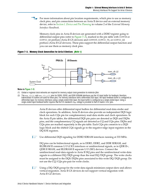
Chapter 7:External Memory Interfaces in Arria II DevicesMemory Interfaces Pin Support for Arria II Devicesf For more information about pin location requirements, which pins to use as memoryclock pins, and pin connections between an Arria II device and an external memorydevice, refer to Section I. Device and Pin Planning in volume 2 of the External MemoryInterface Handbook.Memory clock pins in Arria II devices are generated with a DDIO register going todifferential output pins (refer to Figure7–3), marked in the pin table with DIFFIN orDIFFIO_RX prefixes (Arria II GX devices) and DIFFOUT, DIFFIO_TX, or DIFFIO_RXprefixes (Arria II GZ devices). These pins support the differential output function andyou can use them as memory clock pins.Figure7–3.Memory Clock Generation for Arria II Devices(Note1)Notes to Figure7–3:(1)Global or regional clock networks are required for memory output clock generation to minimize jitter.(2)The mem_clk[0] and mem_clk_n[0] pins for DDR3, DDR2, and DDR SDRAM interfaces use the I/O input buffer for feedback; therefore,bidirectional I/O buffers are used for these pins. For memory interfaces with a differential DQS input, the input feedback buffer is configured as differential input; for memory interfaces using a single-ended DQS input, the input buffer is configured as a single-ended input. Using a single-ended input feedback buffer requires that the I/O standard’s V REF voltage is provided to that I/O bank’s VREF pins.Arria II devices offer differential input buffers for differential read-data strobe andclock operations. In addition, Arria II devices also provide an independent DQS logicblock for each CQn pin for complementary read-data strobe and clock operations. Inthe Arria II pin tables, the differential DQS pin pairs are denoted as DQS and DQSnpins, and the complementary CQ signals are denoted as CQ and CQn pins. DQSn andCQn pins are marked separately in the pin table. Each CQn pin connects to a DQSlogic block and the shifted CQn signals go to the negative-edge input registers in theDQ IOE registers.1Use differential DQS signaling for DDR2 SDRAM interfaces running at 333MHz.DQ pins can be bidirectional signals, as in DDR3, DDR2, and DDR SDRAM, andRLDRAM II common I/O (CIO) interfaces or unidirectional signals, as in QDR II+,QDR II SRAM, and RLDRAM II separate I/O (SIO) devices. Connect theunidirectional read-data signals to Arria II DQ pins and the unidirectional write-datasignals to a different DQ/DQS group than the read DQ/DQS group. The write clocksmust be assigned to the DQS/DQSn pins associated to this write DQ/DQS group. Donot use the CQ/CQn pin-pair for write clocks.1Using a DQ/DQS group for the write-data signals minimizes output skew and allows vertical migration. Arria II GX devices do not support vertical migration withArria II GZ devices.Arria II Device Handbook Volume 1: Device Interfaces and IntegrationChapter 6:I/O Features in Arria II DevicesTermination Schemes for I/O Standardsmini-LVDSArria II GX devices support true mini-LVDS with a three-resistor network using twosingle-ended output buffers for external three-resistor networks.For Arria II GZ devices, use two single-ended output buffers with external one- orthree-resistor networks (mini-LVDS_E_1R or mini-LVDS_E_3R). Arria II GZ row I/Obanks support mini-LVDS output using true LVDS output buffers without an externalresistor network.Figure6–18 shows the one-resistor and three-resistor topology for RSDS andmini-LVDS I/O standard termination.Figure6–18.RSDS and mini-LVDS I/O Standard Termination for Arria II Devices(Note1)Notes to Figure6–18:(1)R p = 170 Ω and R s= 120 Ω(2)mini-LVDS_E_1R is applicable for Arria II GZ devices only.A resistor network is required to attenuate the LVDS output-voltage swing to meetRSDS and mini-LVDS specifications. You can modify the three-resistor networkvalues to reduce power or improve the noise margin. The resistor values chosenshould satisfy the equation shown in Equation6–1.Equation6–1.Resistor Network1To validate that custom resistor values meet the RSDS requirements, Alterarecommends performing additional simulations with IBIS models.f For more information about the RSDS I/O standard, refer to the RSDS Specificationfrom the National Semiconductor website at .f For more information about the mini-LVDS I/O standard, see the mini-LVDSSpecification from the Texas Instruments website at .Arria II Device Handbook Volume 1: Device Interfaces and IntegrationChapter 6:I/O Features in Arria II DevicesArria II OCT CalibrationArria II OCT CalibrationArria II GX devices support calibrated R S OCT and Arria II GZ devices supportcalibrated R S and R T OCT on all I/O pins. You can calibrate the I/O banks with any ofthe OCT calibration blocks available in the device provided the V CCIO of the I/O bankwith the pins using calibrated OCT matches the V CCIO of the I/O bank with thecalibration block and its associated RUP and RDN pins.f For more information about the location of the OCT calibration blocks in Arria IIdevices, refer to the Arria II Device Family Connection Guidelines and Arria II DevicePin-Outs.OCT Calibration BlockAn OCT calibration block has the same V CCIO as the I/O bank that contains the block.R S OCT calibration is supported on all user I/O banks with different V CCIO voltagestandards, up to the number of available OCT calibration blocks. You can configureI/O banks to receive calibrated codes from any OCT calibration block with the sameV CCIO. All I/O banks with the same V CCIO can share one OCT calibration block, even ifthat particular I/O bank has an OCT calibration block.For example, Figure6–10 shows a group of I/O banks that has the same V CCIOvoltage. If a group of I/O banks has the same V CCIO voltage, you can use one OCTcalibration block to calibrate the group of I/O banks placed around the periphery.Because banks 3B, 4C, 6C, and 7B have the same V CCIO as bank 7A, you can calibrateall four I/O banks (3B, 4C, 6C, and 7B) with the OCT calibration block (CB7) locatedin bank 7A. You can enable this by serially shifting out R S OCT calibration codes fromthe OCT calibration block located in bank 7A to the I/O banks located around theperiphery.1I/O banks that do not contain calibration blocks share calibration blocks with I/O banks that do contain calibration blocks.Arria II Device Handbook Volume 1: Device Interfaces and Integration。
FPGA可编程逻辑器件芯片XC7Z020-2CLG400I中文规格书

FPGA Mezzanine (FMC) Card Interface[Figure1-2, callout 24]The ZC702 board supports the VITA 57.1 FPGA Mezzanine Card (FMC) specification [Ref6] by providing subset implementations of low pin count (LPC) connectors at J3 and J4. Both connectors use a 10x40 form factor that is partially populated with 160 pins. Theconnectors are keyed so that a the mezzanine card faces away from the ZC702 board when connected.Connector Type:•Samtec SEAF series, 1.27 mm (0.050 in) pitch. Mates with SEAM series connector.For more information about SEAF series connectors, go to the Samtec website [Ref28].LPC Connectors J3 and J4[Figure1-2, callout 24]The 160-pin FMC LPC connector is shown in Figure B-1.The LPC connections between FMC1 (J3) and XC7Z020 SoC U1 (Table1-28) and between FMC2 (J4) and XC7Z020 SoC U1 (Table1-29) both implement a subset of this connectivity (GTX is not supported):•68 single-ended or 34 differential user-defined signals (34 LA pairs, LA00–LA33)•0GTX transceivers•0GTX clocks• 2 differential clocks•61 ground and 9 power connectionsNote:FMC1 (J3) and FMC2 (J4) GA0 = GA1 = 0 (GND).Table1-28 shows the LPC connections between J3 and XC7Z020 SoC U1.Table 1-28:LPC Connections, FMC1 (J3) to XC7Z020 SoC U1FMC1J3 Pin Net NameI/OStandardXC7Z020(U1) PinFMC1J3 Pin Net NameI/OStandardXC7Z020(U1) PinC2NC D1PWRCTL2_VCC4A_PGC3NC D4NCC6NC D5NCC7NC D8FMC1_LPC_LA01_CC_P LVCMOS25N19 C10FMC1_LPC_LA06_P LVCMOS25J18D9FMC1_LPC_LA01_CC_N LVCMOS25N20 C11FMC1_LPC_LA06_N LVCMOS25K18D11FMC1_LPC_LA05_P LVCMOS25N17The ZC702 board uses power regulators and a PMBus compliant system controller from Texas Instruments to supply core and auxiliary voltages as listed in Table1-30. The Texas Instruments Fusion Digital Power graphical user interface is used to monitor the voltage and current levels of the board power modules.Table 1-30:Onboard Power System DevicesDevice Type ReferenceDesignator Description Power RailNet NamePower RailVoltageSchematicPageCore voltage controller and regulatorsUCD9248PFCU32PMBus Controller–CoreAddr = 52 dec., 0b0110100)39PTD08D210W—VoutAU17Dual 10A 0.6V–3.6V Adj. SwitchingRegulatorVCCINT 1.00V40PTD08D210W—VoutB Dual 10A 0.6V–3.6V Adj. SwitchingRegulatorVCCPINT 1.00V40PTD08D210W—VoutAU18Dual 10A 0.6V–3.6V Adj. SwitchingRegulatorVCCAUX 1.80V41PTD08D210W—VoutB Dual 10A 0.6V–3.6V Adj. SwitchingRegulatorVCCPAUX 1.80V41 Auxiliary voltage controller and regulatorsUCD9248PFCU33PMBus Controller–AuxAddr = 53 dec., 0b0110101)42PTD08D210W—VoutAU19Dual 10A 0.6V–3.6V Adj. SwitchingRegulator(set to 1.8V, 2.5V or 3.3V)VADJ 2.50V43PTD08D210W—VoutB Dual 10A 0.6V–3.6V Adj. SwitchingRegulatorVCC1V5 1.50V43PTD08D210W—VoutAU20Dual 10A 0.6V–3.6V Adj. SwitchingRegulatorVCCMIO_PS 1.80V44PTD08D210W—VoutB Dual 10A 0.6V–3.6V Adj. SwitchingRegulatorVCCBRAM 1.00V44UCD9248PFCU34PMBus Controller–AuxAddr = 54 dec., 0b0110110)45PTD08D210W—VoutAU21Dual 10A 0.6V–3.6V Adj. SwitchingRegulatorVCC3V3 3.30V46PTD08D210W—VoutB Dual 10A 0.6V–3.6V Adj. SwitchingRegulatorVCC2V5/VCC2V5_PL 2.50V46Linear regulatorTPS51200DR U223A Tracking Regulator VTTDDR_PS0.75V37internally OR's these PG conditions together and drives an output PG pin High only if all active rail PG states are “good”. The On and Off Delay and rise and fall times are relative to when the board power on-off slide switch SW12 is turned on and off.Table1-31 defines the voltage and current values for each power rail controlled by theUCD9248 PMBus controller at address 52 decimal (U32).Table 1-31:Power Rail Specifications for UCD9248 PMBus Controller at Address 52 DecimalShutdown Threshold(1)Rail NumberRailName Rail NameNominalVOUT(V)PGOnThreshold(V)PGOffThreshold(V)OnDelay(ms)RiseTime(ms)OffDelay(ms)FallTime(ms)VOUTOverFault(V)IOUTOverFault(A)TempOverFault(°C)1Rail #1VCCINT10.90.8505101 1.152090 2Rail #2VCCPINT10.90.8505101 1.152090 3Rail #3VCCAUX 1.8 1.62 1.530551 2.0710.4190 4Rail #4VCCPAUX 1.8 1.62 1.530551 2.0710.4190Table1-33 defines the voltage and current values for each power rail controlled by the UCD9248 PMBus controller at address 54 decimal (U34).Table 1-33:Power Rail Specifications for UCD9248 PMBus Controller at Address 54 DecimalShutdown Threshold(1)Rail NumberRailNameSchematicRail NameNominalVOUT(V)PGOnThreshold(V)PGOffThreshold(V)OnDelay(ms)RiseTime(ms)OffDelay(ms)FallTime(ms)VOUTOverFault(V)IOUTOverFault(A)TempOverFault(°C)1Rail #1VCC3V3 3.3 2.97 2.8050541 3.79510.4190 2Rail #2VCC2V5 2.5 2.25 2.1250511 2.87510.4190 Notes:1.The values defined in these columns are the voltage, current, and temperature thresholds that causes the regulator to shut。
FPGA可编程逻辑器件芯片EP4CE55F23C7N中文规格书
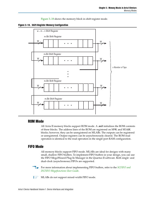
Chapter 3:Memory Blocks in Arria II DevicesMemory Modes Figure3–18 shows the memory block in shift-register mode.Figure3–18.Shift-Register Memory ConfigurationROM ModeAll Arria II memory blocks support ROM mode. A .mif initializes the ROM contentsof these blocks. The address lines of the ROM are registered on M9K and M144Kblocks; however, they can be unregistered on MLABs. The outputs can be registeredor unregistered. Output registers can be asynchronously cleared. The ROM readoperation is identical to the read operation in the single-port RAM configuration.FIFO ModeAll memory blocks support FIFO mode. MLABs are ideal for designs with manysmall, shallow FIFO buffers. To implement FIFO buffers in your design, you can usethe FIFO MegaWizard Plug-In Manager in the Quartus II software. Both single- anddual-clock (asynchronous) FIFOs are supported.f For more information about implementing FIFO buffers, refer to the SCFIFO andDCFIFO Megafunctions User Guide.1MLABs do not support mixed-width FIFO mode.Arria II Device Handbook Volume 1: Device Interfaces and IntegrationChapter 9:Configuration, Design Security, and Remote System Upgrades in Arria II DevicesJTAG ConfigurationYou must connect the nCE pin to GND or drive it low during JTAG configuration. Inmulti-device FPP, AS, and PS configuration chains, the nCE pin of the first device isconnected to GND, while its nCEO pin is connected to nCE of the next device in thechain. The nCE input of the last device comes from the previous device, while its nCEOpin is left floating. In addition, the CONF_DONE and nSTATUS signals are all shared inmulti-device FPP, AS, or PS configuration chains so the devices can enter user mode atthe same time after configuration is complete. When the CONF_DONE and nSTATUSsignals are shared among all the devices, you must configure every device when JTAGconfiguration is performed.1If you only use JTAG configuration, Altera recommends connecting the circuitry as shown in Figure9–17, where each of the CONF_DONE and nSTATUS signals are isolated toenable each device to enter user mode individually.After the first device completes configuration in a multi-device configuration chain,its nCEO pin drives low to activate the nCE pin of the second device, which prompts thesecond device to begin configuration. Therefore, if these devices are also in a JTAGchain, ensure the nCE pins are connected to GND during JTAG configuration or thatthe devices are JTAG configured in the same order as the configuration chain. As longas the devices are JTAG configured in the same order as the multi-deviceconfiguration chain, the nCEO of the previous device drives the nCE of the next devicelow when it has successfully been JTAG configured.You can place other Altera devices that have JTAG support in the same JTAG chain fordevice programming and configuration.1JTAG configuration support is enhanced and allows more than 17 Arria II devices to be cascaded in a JTAG chain.f For more information about configuring multiple Altera devices in the sameconfiguration chain, refer to the Configuring Mixed Altera Device Chains chapter involume2 of the Configuration Handbook.You can configure Arria II devices using multiple configuration schemes on the sameboard. Combining JTAG configuration with a PS or AS configuration on your board isuseful in the prototyping environment because it allows multiple methods toconfigure your FPGA.f For more information about combining JTAG configuration with other configurationschemes, refer to the Combining Different Configuration Schemes chapter in volume2 ofthe Configuration Handbook.Arria II Device Handbook Volume 1: Device Interfaces and IntegrationChapter 3:Memory Blocks in Arria II DevicesDesign ConsiderationsPower-Up Conditions and Memory InitializationM9K and M144K block outputs power up to zero (cleared), regardless of whether theoutput registers are used or bypassed. MLABs power up to zero if the output registersare used and power up reading the memory contents if the output registers are notused. You must take this into consideration when designing logic that might evaluatethe initial power-up values of the MLAB memory block. For Arria II devices, theQuartus II software initializes the RAM cells to zero unless there is a .mif filespecified.All memory blocks support initialization using a .mif. You can create .mif files in theQuartus II software and specify their use with the RAM MegaWizard Plug-InManager when instantiating a memory in your design. Even if a memory ispre-initialized (for example, using a .mif), it still powers up with its outputs cleared.f For more information about .mif files, refer to the Internal Memory (RAM and ROM)Megafunction User Guide and the Quartus II Handbook.Power ManagementArria II memory block clock enables allow you to control clocking of each memoryblock to reduce AC-power consumption. Use the read-enable signal to ensure thatread operations only occur when you need them to. If your design does not requireread-during-write, you can reduce your power consumption by deasserting theread-enable signal during write operations or any period when no memoryoperations occur.The Quartus II software automatically places any unused memory block in low powermode to reduce static power.Arria II Device Handbook Volume 1: Device Interfaces and Integration。
FPGA可编程逻辑器件芯片XQR2V3000-4CG717V中文规格书
FPGA可编程逻辑器件芯⽚XQR2V3000-4CG717V中⽂规格书Summary of QPro? Virtex?-II FeaturesIndustry’s first military-grade platform FPGA solution Certified to MIL-PRF-38535 (Qualified Manufacturer Listing)100% factory testedGuaranteed over the full military temperature range (–55°C to +125°C) or industrial temperature range(–40°C to +100°C)Ceramic and plastic wire-bond and flip-chip grid array packagesIP-immersion architectureDensities from 1M to 6M system gates300+MHz internal clock speed (Advance Data)622+Mb/s I/O (Advance Data)SelectRAM Memory Hierarchy2.5Mb of dual-port RAM in 18Kbit blockSelectRAM resourcesUp to 1Mb of distributed SelectRAM resources High-performance interfaces to external memory DRAM interfaces-SDR/DDR SDRAM-Network FCRAM-Reduced Latency DRAMSRAM interfaces-SDR/DDR SRAM-QDR SRAMCAM interfacesArithmetic functionsDedicated 18-bit x18-bit multiplier blocksFast look-ahead carry logic chainsFlexible logic resourcesUp to 67,584 internal registers/latches with Clock EnableUp to 67,584 look-up tables (LUTs) or cascadable 16-bit shift registersWide multiplexers and wide-input function support Horizontal cascade chain and sum-of-products support Internal 3-state busingHigh-performance clock management circuitryUp to 12 DCM (Digital Clock Manager) modules -Precise clock de-skew-Flexible frequency synthesis-High-resolution phase shifting16 global clock multiplexer buffersActive interconnect technologyFourth-generation segmented routing structurePredictable, fast routing delay, independent offanoutSelectIO-Ultra TechnologyUp to 824 user I/Os19 single-ended and six differential standardsProgrammable sink current (2mA to 24mA) per I/ODigitally Controlled Impedance (DCI) I/O: on-chip termination resistors for single-ended I/O standards PCI compliant (32/33MHz) at 3.3VDifferential signaling622Mb/s Low-Voltage Differential Signaling I/O (LVDS) with current mode driversBus LVDS I/OLightning Data Transport (LDT) I/O with current driver buffersLow-Voltage Positive Emitter-Coupled Logic(LVPECL) I/OBuilt-in DDR input and output registersProprietary high-performance SelectLinkTechnology-High-bandwidth data path-Double Data Rate (DDR) link-Web-based HDL generation methodology ?Supported by Xilinx Foundation Series? and Alliance Series? Development SystemsIntegrated VHDL and Verilog design flowsCompilation of 10M system gates designsInternet Team Design (ITD) toolQPro Virtex-II 1.5V Platform FPGAsDS122 (v3.0) April 7, 2014Product SpecificationSlices LUTs Flip-FlopsMULT_ANDsArithmetic & Carry ChainsSOP Chains Distributed SelectRAM Shift Registers TBUF 488822128bits128bits2Table 17:Virtex-II Logic Resources Available in All CLBsDevice CLB Array: Row x Column Number of Slices Number of LUTs Max Distributed SelectRAM or Shift Register (bits) Number of Flip-Flops Number of Carry Chains (1)Number of SOP Chains (1)XQ2V100040 x 325,12010,240163,84010,2406480XQ2V300064 x 5614,33628,672458,75228,672112128XQ2V6000 96 x 8833,79267,5841,081,34467,584176192Each block SelectRAM cell is a fully synchronous memory, as illustrated in Table 31, page 38. The two ports have independent inputs and outputs and are independently clocked.Port Aspect RatiosT able 20 shows the depth and the width aspect ratios for the 18Kbit block SelectRAM. Virtex-II block SelectRAM also includes dedicated routing resources to provide an efficient interface with CLBs, block SelectRAM, and multipliers. Table 19:Dual-Port Mode ConfigurationsPort A 16K x 116K x 116K x 116K x 116K x 116K x 1Port B16K x 18K x 24K x 42K x 91K x 18512x 36Port A8K x 28K x 28K x 28K x 28K x 2Port B8K x 24K x 42K x 91K x 18512x 36Port A4K x 44K x 44K x 44K x 4Port B4K x 42K x 91K x 18512x 36Port A2K x 92K x 92K x 9Port B 2K x 91K x 18512x 36Port A 1K x 181K x 18Port B 1K x 18512x 36Port A 512x 36Port B512x 36Figure 31:18 Kbit Block SelectRAM in Dual-Port ModeTable 20:18Kbit Block SelectRAM Port Aspect RatioWidth Depth Address Bus Data Bus Parity Bus116,384ADDR[13:0]DA T A[0]N/A 28,192ADDR[12:0]DA TA[1:0]N/A 44,096ADDR[11:0]DA TA[3:0]N/A 92,048ADDR[10:0]DA TA[7:0]Parity[0]181,024ADDR[9:0]DA TA[15:0]Parity[1:0]36512ADDR[8:0]DA TA[31:0]Parity[3:0]。
FPGA可编程逻辑器件芯片EP4CE55F23I7中文规格书

PLLs in Arria II Devices 1When you reconfigure the counter clock frequency, you cannot reconfigure the corresponding counter phase shift settings with the same interface. Instead,reconfigure the phase shifts in real time with the dynamic phase shift reconfiguration interface. If you reconfigure the counter frequency, but want to keep the samenon-zero phase shift setting (for example, 90°) on the clock output, you mustreconfigure the phase shift immediately after reconfiguring the counter clockfrequency.Post-Scale Counters (C0 to C9)You can configure the multiply or divide values and duty cycle of post-scale counters in real time. Each counter has an 8-bit high-time setting and an 8-bit low-time setting.The duty cycle is the ratio of output high- or low-time to the total cycle time, which is the sum of the two. Additionally, these counters have two control bits, rbypass forbypassing the counter and rselodd to select the output clock duty cycle.When the rbypass bit is set to 1, it bypasses the counter, resulting in a divide by 1.When this bit is set to 0, the high- and low-time counters are added to compute the effective division of the VCO output frequency. For example, if the post-scale divide factor is 10, the high- and low-count values could be set to 5and 5, respectively, toachieve a 50-50% duty cycle. The PLL implements this duty cycle by transitioning the output clock from high to low on the rising edge of the VCO output clock. However, a4 and 6 setting for the high- and low-count values, respectively, would produce anoutput clock with a 40-60% duty cycle.The rselodd bit indicates an odd divide factor for the VCO output frequency along with a 50% duty cycle. For example, if the post-scale divide factor is 3, the high- and low-time count values could be set to 2and 1, respectively, to achieve this division.This implies a 67%-33% duty cycle. If you require a 50%-50% duty cycle, you can set the rselodd control bit to 1 to achieve this duty cycle despite an odd division factor.The PLL implements this duty cycle by transitioning the output clock from high tolow on a falling edge of the VCO output clock. When you set rselodd=1,yousubtract 0.5 cycles from the high time and you add 0.5cycles to the low time. Forexample:■High-time count = 2 cycles■Low-time count = 1 cycle■rselodd = 1 effectively equals:■High-time count = 1.5 cycles■Low-time count = 1.5 cycles■Duty cycle = (1.5/3) % high-time count and (1.5/3)% low-time countDocument Revision History PLL Specificationsf For more information about PLL timing specifications, refer to the Device Datasheet forArria II Devices.Document Revision HistoryTable5–23 lists the revision history for this chapter.Table5–23.Document Revision HistoryDate Version ChangesJuly 2012 4.2Updated “Periphery Clock Networks” section.June 2011 4.1■Updated Table5–15.■Updated Figure5–44.■Updated “Dynamic Phase-Shifting” section.■Added Figure5–5, Figure5–6, Figure5–7, and Figure5–8.■Minor text edits.December 2010 4.0■Updated for the Quartus II software version 10.1 release.■Added Arria II GZ devices information.■Updated Table5–1, Table5–12, Table5–20, and Table5–21.■Added Figure5–2, Figure5–3, Figure5–4, Figure5–5, Figure5–7, Figure5–15, Figure5–11, Figure5–16, Figure5–18, Figure5–19, Figure5–24, Figure5–26, Figure5–27, Figure5–38, and Figure5–39.■Added Table5–5, Table5–7, Table5–9, Table5–11, andTable5–16.■Added “Clock Sources Per Quadrant” and “External Feedback Mode” sections.■Minor text edit.July 2010 3.0Updated for Arria II GX v10.0 release:■Updated “Clock Regions” and “Arria II PLL Hardware Overview” sections.■Updated Figure5–44.■Removed sub-regional clock references.■Minor text edit.November 2009 2.0Updated for Arria II GX v9.1 release:■Updated Table5–1.■Updated Figure5–14.■Updated the “Periphery Clock (PCLK) Networks” and “Cascading PLLs” sections.■Minor text edit.June 2009 1.1■Updated Table5–8.■Updated Figure5–13 and Figure5–14.■Updated the “PLL Clock I/O Pins” and “PLL Reconfiguration Hardware Implementation”sections.February 2009 1.0Initial releaseI/O Banks Arria II GZ devices contain up to 20 I/O banks as shown in Figure6–2. Each I/O bankcan support high-performance external memory interfaces with dedicated circuitry.The I/O pins are organized in pairs to support differential standards. Each I/O pinpair can support both differential input and output buffers except the clk[1,3,8,10],PLL_L[1,4]_clk, and PLL_R[1,4]_clk pins, which support differential inputoperations only.Figure6–2.I/O Banks in Arria II GZ Devices(Note1), (2), (3), (4), (5), (6), (7), (8)Notes to Figure6–2:(1)Differential HSTL and SSTL outputs are not true differential outputs. They use two single-ended outputs with the second output programmed asinverted.(2)Column I/O differential HSTL and SSTL inputs use LVDS differential input buffers without R D OCT support.(3)Column I/O supports LVDS outputs using single-ended buffers and external resistor networks.(4)Column I/O supports PCI/PCI-X with an on-chip clamp diode. Row I/O supports PCI/PCI-X with an external clamp diode.(5)Clock inputs on column I/Os are powered by V CCCLKIN when configured as differential clock inputs. They are powered by V CCIO when configured assingle-ended clock inputs. All outputs use the corresponding bank V CCIO.(6)Row I/O supports the true LVDS output buffer.(7)Column and row I/O banks support LVPECL standards for input clock operation.(8)Figure6–2 is a top view of the silicon die that corresponds to a reverse view for flip chip packages. It is a graphical representation only.。
FPGA可编程逻辑器件芯片EP4CE40F23C7中文规格书

Figure5–30 shows an example waveform of the phase relationship between the PLLclocks in external feedback mode.Figure5–30.Phase Relationship Between the PLL Clocks in External Feedback Mode for Arria II DevicesNote to Figure5–30:(1)The PLL clock outputs can lead or lag the fbin clock input.Figure5–31 shows external feedback mode implementation in Arria II GZ devices. Figure5–31.External Feedback Mode in Arria II GZ DevicesClock Multiplication and DivisionEach Arria II PLL provides clock synthesis for PLL output ports withM/(N post-scale counter) scaling factors. The input clock is divided by a pre-scalefactor (n) and is then multiplied by the m feedback factor. The control loop drives theVCO to match f in (M/N). Each output port has a unique post-scale counter thatdivides down the high-frequency VCO. For multiple PLL outputs with differentfrequencies, the VCO is set to the least common multiple of the output frequenciesthat meets its frequency specifications. For example, if output frequencies requiredfrom one PLL are 33 and 66MHz, the Quartus II software sets the VCO to 660MHz(the least common multiple of 33 and 66 MHz in the VCO range). Then the post-scalecounters scale down the VCO frequency for each output port.Manual Clock Switchover ModeIn manual clock switchover mode, the clkswitch signal controls whether inclk0 orinclk1 is selected as the input clock to the PLL. By default, inclk0 is selected. Alow-to-high transition on clkswitch and being held high for at least three inclk cycles begins a clock switchover event. You must bring the clkswitch signal back low again to perform another switchover event in the future. If you do not require anotherswitchover event in the future, you can leave clkswitch in a logic high state after the initial switch. Pulsing clkswitch high for at least three inclk cycles performs another switchover event. If inclk0 and inclk1 are different frequencies and are alwaysrunning, the clkswitch minimum high time must be greater than or equal to three of the slower frequency inclk0 and inclk1 cycles.Figure 5–37 shows a block diagram of the manual switchover circuit.f For more information about PLL software support in the Quartus II software, refer tothe Phase-Locked Loops (ALTPLL) Megafunction User Guide .Clock Switchover GuidelinesUse the following guidelines when implementing clock switchover in Arria II PLLs.■Automatic clock switchover requires that the inclk0 and inclk1 frequencies be in100% (2x) of each other. Failing to meet this requirement causes the clkbad[0] andclkbad[1] signals to not function properly.■When you use manual clock switchover mode, the difference between inclk0 andinclk1 can be more than 100% (2x). However, differences in frequency, or phase ofthe two clock sources, or both, are likely to cause the PLL to lose lock. Resetting thePLL ensures that the correct phase relationships are maintained between the inputand output clocks.1Both inclk0 and inclk1 must be running when the clkswitch signal goeshigh to start the manual clock switchover event. Failing to meet thisrequirement causes the clock switchover to not function properly.■Applications that require a clock switchover feature and a small frequency driftmust use a low-bandwidth PLL. The low-bandwidth PLL reacts more slowly thanthe high-bandwidth PLL to reference the input clock changes. When theswitchover event occurs, a low-bandwidth PLL propagates the stopping of theclock to the output more slowly than the high-bandwidth PLL. However, be awarethat the low-bandwidth PLL also increases lock time.Figure 5–37.Manual Clock Switchover Circuitry in PLLs for Arria II DevicesPLLs in Arria II DevicesCharge Pump and Loop FilterYou can reconfigure the charge pump and loop filter settings to update the PLL bandwidth in real time. Table5–17 through Table5–19 show the possible settings for charge pump current (Icp), loop filter resistor (R), and capacitor (C) values for Arria II PLLs.Table5–17.charge_pump_current Bit Settings for Arria II DevicesCP[2]CP[1]CP[0]Decimal Value for Setting0000001101131117Table5–18.loop_filter_r Bit Settings for Arria II DevicesLFR[4]LFR[3]LFR[2]LFR[1]LFR[0]Decimal Value for Setting0000000001130010040100081000016100111910100201100024110112711100281111030Table5–19.loop_filter_c Bit Settings for Arria II DevicesLFC[1]LFC[0]Decimal Value for Setting 000011113。
FPGA可编程逻辑器件芯片10M08DAF256C7G中文规格书
0 Disable Interrupt (Mask)
1 Enable Interrupt (Unmask)
ADSP-BF70x Blackfin+ Processor Hardware Reference
0 Disable Interrupt (Mask)
1 Enable Interrupt (Unmask)
4 WUIM (R/W)
Wake Up Interrupt Mask. The CAN_GIM.WUIM bit enables (unmasks) the wake up interrupt.
0 Disable Interrupt (Mask)
1 Enable Interrupt (Unmask)
3 BOIM (R/W)
Bus Off Interrupt Mask. The CAN_GIM.BOIM bit enables (unmasks) the bus off interrupt.
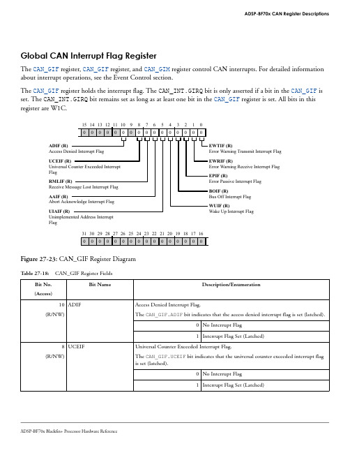
15 14 13 12 11 10 9 8 7 6 5 4 3 2 1 0 0000000000000000
ADIF (R) Access Denied Interrupt Flag
UCEIF (R) Universal Counter Exceeded Interrupt Flag
RMLIF (R) Receive Message Lost Interrupt Flag
ADSP-BF70x CAN Register Descriptions
Global CAN Interrupt Flag Register
The CAN_GIF register, CAN_GIF register, and CAN_GIM register control CAN interrupts. For detailed information about interrupt operations, see the Event Control section.
- 1、下载文档前请自行甄别文档内容的完整性,平台不提供额外的编辑、内容补充、找答案等附加服务。
- 2、"仅部分预览"的文档,不可在线预览部分如存在完整性等问题,可反馈申请退款(可完整预览的文档不适用该条件!)。
- 3、如文档侵犯您的权益,请联系客服反馈,我们会尽快为您处理(人工客服工作时间:9:00-18:30)。
The AD823A is a dual precision, 17 MHz, JFET input op amp manufactured in the extra fast complementary bipolar (XFCB) process. The AD823A can operate from a single supply of 3 V to 36 V or from dual supplies of ±1.5 V to ±18 V. It has true single-supply capability with an input voltage range extending below ground in single-supply mode. Output voltage swing extends to within 20 mV of each rail for IOUT ≤ 100 μA, providing outstanding output dynamic range. It also has a linear output current of 40 mA, 0.5 V from the supply rails.
Table 8 shows the noise sources and total output noise for the photodiode preamp, where the preamplifier is configured to have a 45° phase margin for maximal bandwidth and fz = fx = fn in this case.
APPLICATIONS
Photodiode preamps Active filters 12-bit to 16-bit data acquisition systems Medical instrumentation Precision instrumentation
GENERAL DESCRIPTION
ACTIVE FILTER
The AD823A is an ideal candidate for an active filter because of its low input bias current and its low input capacitance. Low input bias current reduces dc error in the signal path while low input capacitance improves the accuracy of the active filter.
49.9kΩ +5V
photodiode preamp. The noise bandwidth is at the frequency fN,
and it can be calculated by
0.1µF
–5V
AD823A
VOUT
fN
=
(CS
+
fu CF
)
CF
(6)
0.1µF
100Ω
09439-050
1.2pF
photodiode preamp design are the input voltage noise of the amplifier, VNOISE and the resistor noise due to RF. The gray curve in Figure 43 shows the noise gain over frequencies for the
Data Sheet
FEATURES
Single-supply operation Output swings rail-to-rail Input voltage range extends below ground Single-supply capability from 3 V to 36 V
High load drive Capacitive load drive of 470 pF (G = +1, 25% overshoot) Linear output current of 40 mA, 0.5 V from supplies
Excellent ac performance on 2.6 mA/amplifier −3 dB bandwidth of 17 MHz, G = +1 325 ns settling time to 0.01% (2 V step) Slew rate of 30 V/μs Low distortion: −108 dBc at 20 kHz (G = −1, RL = 2 kΩ)
0°
f
log f
–45°
–90°
09439-400
(A) WITHOUT COMPENSATION
–135°
(B) WITH COMPENSATION
Figure 43. Gain and Phase Plot of the Transimpedance Amplifier Design
The dominant sources of output noise in the wideband
AD823A
CONNECTION DIAGRAM
09439-001
OUT1 1 –IN1 2
+IN1 3
–VS 4
AD823A
8 +VS 7 OUT2 6 –IN2 5 +IN2
Figure 1. 8-Lead SOIC
09439-102
AD823A
OUT1 1 –IN1 2 +IN1 3 –VS 4
85
1k
10k
100k
1M10MFra bibliotekFREQUENCY (Hz)
Figure 45. Photodiode Preamplifier Frequency Response
09439-144
AD823A
Data Sheet
Table 8. RMS Noise Contributions of Photodiode Preamp
OPEN-LOOP GAIN
OPEN-LOOP GAIN
AD823A
|A (s)|
|A| (dB)
fx
G=1
G = R2C1s
fp
log f fu
I TO V GAIN
G=1 fp
fx
fz
fn
G = RFCS(s)
G = 1 + CS/CF
f fu
0°
90°
–45°
45°
PHASE (°)
–90° –135° –180°
The AD823A is available over the industrial temperature range of −40°C to +85°C and is offered in an 8-lead SOIC package and an 8-lead MSOP package.
Data Sheet
Good dc performance 700 μV maximum input offset voltage 1 μV/°C offset voltage drift 25 pA maximum input bias current
Low noise: 14 nV/√Hz at 10 kHz No phase inversion with inputs to the supply rails
TRANSIMPEDANCE GAIN (dB)
–5V
Figure 44. Photodiode Preamplifier
95
94
93
92
IPHOTO = 1µA p-p CF = 2.7pF
91
90
IPHOTO = 1µA p-p
89
CF = 1.2pF
88
87
86
Rev.B | Page 17 of 20
This combination of ac and dc performance, plus the outstanding load drive capability, results in an exceptionally versatile amplifier for applications such as ADC drivers, high speed active filters, and other low voltage, high dynamic range systems.