BT1207S-P蓝牙模块规格书1.2
NCP1207在电源适配器中的应用

maxVflb V kV flbbuklm k i n11 21 2 74 71 0.47
变压器初级绕组的峰值电流为:
Ipp k2Im in aavx g260.4 4 17 0 3 02.7A 2
最低输入电压时,功率转换器的开关频率为最低设定70KHZ .最大导通时间为:
10 ~ 7
2UEW-φ0.40×2
线圈结构图:
圈数 38 8 12 8 18
绕制方法 双线并绕 均匀散绕 三线并绕 三线并绕 双线并绕
初级线圈电流控制:
初级电感量为:
LpV bIp um p lkkitnON 2 1 .7 .42 61 .710 634 u7 H (实际值为:400uH) 变压器铁芯电感系数AL:
AL
Lp (np)2
0.34.1703 (5)52
11n5H
24VDC输出绕组的圈数为:
n sV sm (1 a V b x m u )m a n lp x ki n(2 4 1 0 ).4 (1 1 7 0 .4 4 )7 5 1 5 1t2 urns
安森美的NCP1207是一款专著于反激、电流模、 准谐振模式PWM控制器。 由NCP1207构成的离线式功率变换器用于消费电子产品是一不错的选择。 如用在笔记本电脑电源适配器、离线式电池充电器、DVD电源供应器、 机顶盒电源等。 同时,由于NCP1207工作在准谐振模式,用于消费类小功率电子产品的电源中, 电源的电磁骚扰明显减小,电源在轻载时效率可高于是70%,同时它还可以用 于反激式同步整流,更进一步提高电源的较率。
12VDC输出绕组的圈数为:
n s 1 .3 .V s m (1 a V b m xu ) m n alp x ki n (1 2 1 0 ).4 (1 1 0 7 .4 4 )7 5 1 .1 5 .3 8 turns
深圳市昇润科技HY-40R201低功耗蓝牙5.0模块规格书说明书

HY-40R201深圳昇润科技对本手册中可能出现的和/或规格书的权利,恕不另行通知用作生命支持设备或系统中的关键标是由美国蓝牙SIG公司所有.R201低功耗蓝牙 5.0模块规格书(40 pin)文档版本:V2.02017年10月25日深圳市昇润科技有限公司版权所有现的错误不承担责任。
此外,昇润科技保留随时行通知,并不承诺更新此处所包含的信息。
昇润的关键组件。
以及不承担各种专利或知识产权的.密级:公开资料留随时更改硬件,软件。
昇润的产品不被授权产权的授权使用;蓝牙商1.简述 (1)1-1应用: (1)1-2主要特征: (1)2. 产品型号 (2)2-1.(4 种天线形式可供选择)/( 可选: 带屏蔽罩或不带屏蔽罩) (2)2-2: HY-40R201PC机种屏蔽罩上FCC ID &( IC ID 待定义)印刷内容: (2)3. 模块尺寸与图片 (2)3.1 HY-40R201P / WMD40R201SR6P0 PCB IFA天线 (2)3-2.HY-40R201I /WMD40R201SR6I0 IPEX RF外接天线连接端子 (3)3-3. HY-40R201W / MD40R201SR6W0 金属线天线 (1/4波长偶极子天线) (3)3.4. HY-40R201C/ WMD40R201SR6C0 (陶瓷天线) (3)(4). 应用注意事项: (4)5.引脚分配和端口功能说明 (5)6. 电气特性 (6)6-1. 射频特性 及 电流功耗: (6)6-2. 绝对最大额定值 (7)6-3. ESD 额定值 (7)6-4.建议工作条件 (7)6-5.GPIO DC特性 (7)6-6. 时序要求 (8)6-7. 动作状态切换时序特性 (8)7. 模块方块图 (8)8.IC功能方块图 (9)9. 工作模式架构图 (9)10. 回流焊曲线建议 (无铅锡膏: Sn 96.5%, Ag 3%, Cu 0.5%) (10)11. HY-40R201PC / WMD40R201SR6PC 模块 FCC及 IC声明 (11)12.联系我们 (13)HY-40R201提供蓝牙低功耗特性:无线电,蓝牙协议栈,配置文件和客户应用程序的所需空间。
BT-120中文资料
©2008 Amp’ed RF Inc
1722 Ringwood Ave, Suite 250, San Jose, CA 95131, USA
BT-120/121 Datasheet Page 5 of 6
元器件交易网
Amp’ed RF, Inc.
元器件交易网
Amp’ed RF, Inc.
(phone) 408 213-9530 (fax) 408 213-9533
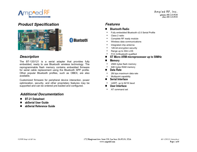
Product Specification
Features
Bluetooth Radio
Fully embedded Bluetooth v2.0 Serial Profile Class 2 radio Complete RF ready module Wireless data communications Integrated chip antenna 128-bit encryption security Range up to 30m LOS FCC & Bluetooth qualified
1722 Ringwood Ave, Suite 250, San Jose, CA 95131, USA
BT-120/121 Datasheet Page 4 of 6
元器件交易网
Amp’ed RF, Inc.
(phone) 408 213-9530 (fax) 408 213-9533
BT-120/121 Datasheet Page 2 of 6
元器件交易网
Amp’ed RF, Inc.
(phone) 408 213-9530 (fax) 408 213-9533
Serial Interface AT Commands
BLF7G20LS-140P,118;BLF7G20LS-140P,112;中文规格书,Datasheet资料
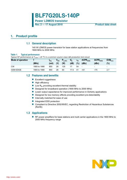
BLF7G20LS-140PPower LDMOS transistorRev. 2 — 17 August 2010Product data sheet 1. Product profile1.1General description140W LDMOS power transistor for base station applications at frequencies from1800MHz to 2000MHz.Table 1.Typical performanceTypical RF performance at T case = 25 °C in a common source class-AB production test circuit.Mode of operation f I Dq V DS P L(AV)G pηD ACPR400k ACPR600k EVM rms (MHz)(mA)(V)(W)(dB)(%)(dBc)(dBc)(%)CW1805to1880850281251754---GSM EDGE1805to1880850286017.541−61−75 2.71.2Features and benefitsExcellent ruggednessHigh efficiencyLow R th providing excellent thermal stabilityDesigned for broadband operation (1800 MHz to 2000 MHz)Lower output capacitance for improved performance in Doherty applicationsDesigned for low memory effects providing excellent pre-distortabilityInternally matched for ease of useIntegrated ESD protectionCompliant to Directive 2002/95/EC, regarding Restriction of Hazardous Substances(RoHS)1.3ApplicationsRF power amplifiers for base stations and multi carrier applications in the 1800 MHz to 2000 MHz frequency range2. Pinning information[1]Connected to flange.3. Ordering information4. Limiting values5. Thermal characteristicsTable 2.PinningPin Description Simplified outlineGraphic symbol1drain12drain23gate14gate25source[1]4532143sym117Table 3.Ordering informationType numberPackageName DescriptionVersion BLF7G20LS-140P -earless flanged LDMOST ceramic package; 4leadsSOT1121BTable 4.Limiting valuesIn accordance with the Absolute Maximum Rating System (IEC 60134).Symbol ParameterConditionsMin Max Unit V DS drain-source voltage -65V V GS gate-source voltage −0.5+13V T stg storage temperature −65+150°C T jjunction temperature-200°CTable 5.Thermal characteristics Symbol ParameterConditionsTypUnit R th(j-c)thermal resistance from junction to caseT case =80°C; P L =100W0.41K/W6. Characteristics7. Test information7.1Ruggedness in class-AB operationThe BLF7G20LS-140P is capable of withstanding a load mismatch corresponding to VSWR =10 : 1 through all phases under the following conditions: V DS =28V; I Dq =850mA;P L =140W (CW); f =1805MHz.Table 6.CharacteristicsT j = 25 °C; per section unless otherwise specified.Symbol ParameterConditionsMin Typ Max Unit V (BR)DSS drain-source breakdown voltage V GS =0V; I D =0.9mA 65--V V GS(th)gate-source threshold voltage V DS =10 V; I D =90mA 1.5 1.9 2.3V I DSS drain leakage current V GS =0V; V DS =28V --2μA I DSX drain cut-off current V GS =V GS(th)+3.75 V; V DS =10V14--A I GSS gate leakage current V GS =11V; V DS =0V --200nA g fs forward transconductance V DS =10V; I D =2.5A - 6.45-S R DS(on)drain-source on-state resistanceV GS =V GS(th) + 3.75V; I D =3.15A-0.15-ΩTable 7.Application informationf = 1805 MHz and 1880 MHz; RF performance at V DS = 28 V; I Dq =850mA; T case = 25 °C; 2sections combined unless otherwise specified; in a class-AB production test circuit.Symbol Parameter ConditionsMin Typ Max Unit Mode of operation: GSM EDGE; P L(AV) = 60 WG p power gain 16.317.5-dB RL in input return loss -−15−8dB ηDdrain efficiency3741-%ACPR 400k adjacent channel power ratio (400 kHz)-−61−56.5dBc ACPR 600k adjacent channel power ratio (600 kHz)-−75−69.5dBc EVM rms RMS EDGE signal distortion error - 2.7 4.0%EVM M peak EDGE signal distortion error -8.512.5%Mode of operation: CW; P L(AV) = 125 WG p power gain 1617-dB ηDdrain efficiency4854-%7.2One-tone CW7.3Two-tone CW7.4GSM EDGE7.5Single carrier IS-95Single carrier IS-95 with pilot, paging, sync and 6traffic channels (Walsh codes 8-13).PAR=9.7dB at 0.01% probability on the CCDF. Channel bandwidth is 1.2288MHz.7.6Single carrier W-CDMA3GPP; test model1; 64DPCH; PAR=7.2dB at 0.01% probability on CCDF.Channel bandwidth is 3.84MHz.7.7Test circuitTable 8.List of componentsFor test circuit see Figure12.Component Description Value Remarks C1, C2, C3multilayer ceramic chip capacitor24pF[1]C4, C5multilayer ceramic chip capacitor 4.7 μF[2]C6, C7, C8multilayer ceramic chip capacitor11pF[3]C9, C10multilayer ceramic chip capacitor10 μF[2]C11electrolytic capacitor470 μF; 63 VR1, R2SMD resistor12ΩPhilips 1206[1]American Technical Ceramics type 100A or capacitor of same quality.[2]TDK or capacitor of same quality.[3]American Technical Ceramics type 100B or capacitor of same quality.7.8Impedance informationTable 9.Typical impedanceTypical values valid for both section in parallel unless otherwise specified.f Z S Z LMHzΩΩ1800 1.1 − j3.8 1.8 − j2.8 1840 1.3 − j3.7 1.7 − j2.6 1880 1.2 − j3.8 1.6 − j2.58. Package outlineFig 14.Package outline SOT1121B9. Abbreviations10. Revision historyTable 10.AbbreviationsAcronym Description CW Continuous WaveEDGE Enhanced Data rates for GSM Evolution ESD ElectroStatic DischargeGSM Global System for Mobile communications IS-95Interim Standard 95LDMOS Laterally Diffused Metal Oxide SemiconductorLDMOST Laterally Diffused Metal Oxide Semiconductor Transistor RF Radio Frequency SMD Surface Mounted Device VSWR Voltage Standing Wave RatioW-CDMAWideband Code Division Multiple AccessTable 11.Revision historyDocument ID Release date Data sheet status Change notice Supersedes BLF7G20LS-140P v.220100817Product data sheet-BLF7G20L-140P_7G20LS-140P v.1Modifications:•This document now only describes the BLF7G20LS-140P .•Table 1 on page 1: changed some values.•Table 4 on page 2: removed drain current specification.•Table 6 on page 3: added typical value for g fs .•Table 7 on page 3: changed some values.•Section 7.2 on page 4: updated the figures.•Section 7.3 on page 4: updated the figures.•Section 7.4 on page 5: updated the figures.•Section 7.5 on page 6: updated the figures.BLF7G20L-140P_7G20LS-140P v.120100421Objective data sheet--分销商库存信息:NXPBLF7G20LS-140P,118BLF7G20LS-140P,112。
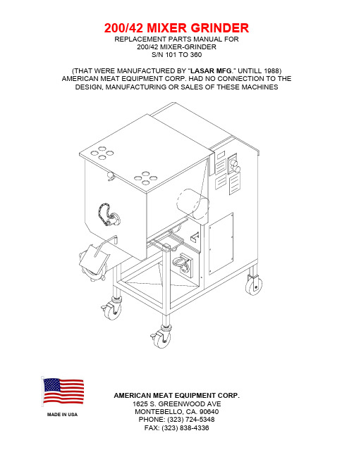
200 42混合器机器人替代部件和配件手册说明书
0040310
200 SPURT GUARD
SS 200 FRAME (P.O.R.)
0090638
KNOB
0040138 LID LOCK HOOK W/NUT
0058116 BRACKET FRONT (PLATED)
0058116S SS BRACKET FRONT
0058117
SS SHAFT FRONT
TOOL PAN ACCESS COVER SWITCH HOLDER GEAR BOX MOUNT
BELT COVER BEARING BRACKET WITH BUSHING
BUSHING BEARING BRACKET
QTY.
1 1 1 1 1 2 1 1 1
PAGE 6
200/42 MIXER GRINDER
42 KNIFE (INVESTMENT) 42 KNIFE (PREMIUM) 42-1/8” HOLE PLATE 42-3/16” HOLE PALTE 42-1/4” HOLE PLATE
QTY.
1 1 1 A/R 1 1 1 1 1 1 1 1
ITEM#
9D 10 10 11 12 13 14 15 16 17 18
QTY. 1 1 1 2 2 2 2 2 2 2 2
PAGE 4
1 5 6 3
200/42 MIXER GRINDER
REPLACEMENT PADDLE ASSEMBLY & BUSHING
FOR 200 MIXER GRINDERS S/N 101 TO 360
(THAT WERE MANUFACTURED BY “LASAR MFG.”)
BTS840S2中文资料

Infineon technologies
2
2003-Oct-01
元器件交易网
BTS 840 S2
Maximum Ratings at Tj = 25°C unless otherwise specified
Parameter
Symbol
Supply voltage (overvoltage protection see page 5)
see diagrams on page 10
Electrostatic discharge capability (ESD)
IN:
(Human Body Model)
ST, IS:
out to all other pins shorted:
acc. MIL-STD883D, method 3015.7 and ESD assn. std. S5.1-1993
-10 ... +16 V ±2.0 mA ±5.0 ±14
1) Supply voltages higher than Vbb(AZ) require an external current limit for the GND and status pins a 150Ω
resistor for the GND connection is recommended.
Symbol Vbb
3 7 16,17, 18,19 12,13, 14,15
IN1 IN2 OUT1
OUT2
4
ST1
8
ST2
2
GND1
6
GND2
5
IS1Vbb
Function Positive power supply voltage. For high
(完整word版)科蒂斯控制器1207A说明书(中)
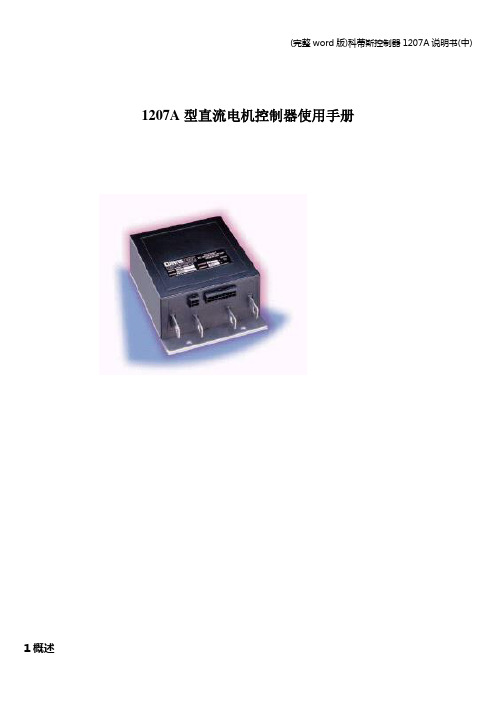
1207A型直流电机控制器使用手册1概述CURTIS PMC 1207A可编程电机速度控制器为各种小型电动车辆提供了高效和易于安装的的控制系统,典型的应用对象为行走式叉车/堆垛车,小型载客车和清洁车等,以微控制器为核心的逻辑部分,配以可靠的MOSFET功率单元,为封装简洁紧凑的1207A控制器提供了大功率输出和先进的性能,可选用手持式编程器使用户能进行快捷、方便地完成参数设定,指导调试及获取故障诊断信息。
同所有CURTIS PMC 电机速度控制器一样,1207A型控制器为车辆的电机驱动速度提供了优异的运动控制,1207A控制器的主要性能包括:◆无级变速和反相制动控制◆大功率MOSFET设计提供高效(减少电机和电池损耗)和无噪声操作◆纯铜功率母线,配以经极化处理接线器传输能量◆采用铝制安装板和注模外壳,具有坚固而保护良好的结构◆过电压和欠电压保护可有效。
◆温度保护和补偿电路提供了低温消减,恒定电流限幅及高温线性回落功能一因而在任何温度条件下都不会发生突然性功率输出中断。
◆智能型手持编程器(选用件)提供了一套完整的参数设定和功能设定◆控制器及其它系统部件的诊断与测试信息,既能够通过车辆上的控制器获得,也可通过编程器获得◆硬件电路和软件对调速器电路,MOSFET驱动电路,MOSFET晶体管,接触器驱动器和接触器进行故障检测—-—确保控制器满足欧洲经济共同体(EEC)所规定的故障检测要求。
◆输入顺序选择包括空档起动和SRO◆微处理器控制的接触器动作顺序提供了真正的无电弧接触器开闭◆平滑的, 可控的反相制动—可变方式(与调速器位置相关)或固定的反相电流限幅方式◆空挡制动功能。
◆双模式运行可使车辆在不同环境下有不同的运行特性。
◆单信号输入方式的紧急反向功能(凸键开关)◆防后滑功能提供了满功率斜坡起动◆简洁的接触器和开关接线,带有短路和开路监测的线圈驱动器确保了安全操作。
◆灵活的调速器电路能够适应各种类型的调速器:5000-0欧姆,0-5000欧姆,0-5伏,3线电位器和各种电子调速器熟悉CURTIS PMC控制器会帮助您正确地安装和使用它。
Silabs BT122 Bluetooth Dual Mode模块项目配置指南说明书
UG496: BT122 Project Configuration User’s GuideThis document walks you through how to start a software projectfor your BT122 Bluetooth Dual Mode module, how to include the necessary resources in the project and also how to configure the hardware interface settings for the Bluetooth modules.KEY FEATURES•BT122 Project structure•Precise description of attributes and syntax used inside project files.Table of Contents1. Project Structure (3)1.1 Project File (3)1.2 Hardware Configuration (3)1.3 Bluetooth Low Energy Service Database (3)1.4 Bluetooth BR/EDR Profile SDP Entries (3)1.5 BGScript Application Code (3)1.6 Host Application Code (3)2. Project File Syntax (4)2.1 <project> (4)2.2 <hardware> (4)2.3 <gatt> (4)2.4 <script> (5)2.5 <image> (5)2.6 <entry> (6)2.7 <library> (6)2.8 Examples (7)2.8.1 Basic Project File for BT122 Bluetooth Dual Mode Module without a BGScript Application: (7)2.8.2 Basic Project File for BT122 Bluetooth Dual Mode Module Including a BGScript Application..73. Hardware Configuration File (8)3.1 <adc> (8)3.2 <sleep> (8)3.3 <controller sleep> (9)3.4 <wakeup pin> (10)3.5 <port> (11)3.6 <uart> (13)3.7 <i2c> (14)3.8 <host wakeup> (15)3.9 <bridging> (15)3.10 <lfxo> (15)4. SPP Configuration File (16)5. DID Configuration File (17)6. HID Configuration File (18)7. Revision History (21)The figure below illustrates the Bluetooth software project structure and the mandatory and optional resources. The structure is relative-ly simple and consists of the following components:1.Project file.2.Hardware configuration file.3.Bluetooth Low Energy service and characteristics database (GATT database).4.Bluetooth BR/EDR profile SDP entries.5.BGScript application source code (optional).6.Host application source code (optional and exclusive to BGScript code).1.1 Project FileThe project file defines the resources included in the project and their physical locations.1.2 Hardware ConfigurationThe hardware configuration file defines the host and peripheral interfaces (like UART, I2C and GPIO) used by the application and their settings.1.3 Bluetooth Low Energy Service DatabaseThe service database (GATT database) defines the contents and structure of the Bluetooth GATT services and characteristics imple-mented by the application. The GATT database is defined with the Profile Toolkit™ ― an XML-based description language1.4 Bluetooth BR/EDR Profile SDP EntriesThe SDP entries define the content of the Service Discovery Profile database for Bluetooth BR/EDR profiles like Serial Port Profile, Human Interface Device Profile, Apple iAP2 profile, or Device Information Profile.1.5 BGScript Application CodeBGScript is a basic-style application scripting language, which allows simple applications to be embedded into the BT122 Bluetooth Dual Mode module. When BGScript is used to implement the application logic, the source file needs to be included in the Bluetooth project file.1.6 Host Application CodeAn alternative way to implement the application is to use an additional host (typically an MCU) and use the Bluetooth module as a mo-dem. In this case, the application code runs outside the module and the source code files do not need to be included in the Bluetooth project, but the architecture selection needs to be defined in the project file.The project file (typically project.xml) describes all the components included in your Bluetooth Dual Mode project. Typically, these files are named as follows:•hardware.xml – Hardware configuration file for interfaces like UART and I2C•GATT.xml – GATT database file for Bluetooth Low Energy services and characteristics configuration•DID.xml, SPP.xml, HID.XML, etc. – SDP entry file(s) for possible Bluetooth profiles•script.bgs – Optional BGScript application source codeThe project file also defines other settings of the project like the hardware version or the firmware output files.The project file itself is a simple XML file with only a few elements in it, which are described below.2.1 <project>The XML attribute <project> starts the definition of the project file and includes the hardware device type the project is meant for. All the2.2 <hardware>The XML attribute <hardware> with its in parameterdefines the hardware configuration of the device.2.3 <gatt>The XML attribute <gatt> with its in parameter defines the GATT database file.Note: The GATT definition can also be placed inside Project XML file.The optional XML attribute <script> and its in parameters define the BGScript source code file. This XML attribute is placed within the2.5 <image>The XML attribute <entry> and its parameters are used to define the actual XML files for each of the Bluetooth BR/EDR SDP static records that you want to include in the firmware.These XML attributes are grouped within an XML attribute pair <sdp></sdp> which is used to define the Bluetooth BR/EDR Service2.7 <library>The optional XML attribute <library> and its in parameter are used to select which of the available variants of the software is to be built. The XML attribute is placed within the XML attribute pair <software></software>. This tag is not mandatory, if omitted the default library2.8.1 Basic Project File for BT122 Bluetooth Dual Mode Module without a BGScript Application:<?xml version="1.0" encoding="UTF-8" ?><!-- Project configuration including BT122 device type --><!-- XML file containing GATT service and characteristic definitions both for BLE and GATT over BR/EDR--> <gatt in="gatt.xml" /><!-- Local hardware interfaces configuration file --><hardware in="hardware.xml" /><!-- Local SDP entries for Bluetooth BR/EDR --><sdp><entry file="DID.xml" autoload="true"/><entry file="SPP.xml" id="2"/></sdp><!-- Firmware output files --><image out="BT122_BGDemo.bin"/></project>2.8.2 Basic Project File for BT122 Bluetooth Dual Mode Module Including a BGScript Application<?xml version="1.0" encoding="UTF-8" ?><!-- Project configuration including BT122 device type --><project device="bt122"><!-- XML file containing GATT service and characteristic definitions both for BLE and GATT over BR --><gatt in="gatt.xml" /><!-- Local hardware interfaces configuration file --><hardware in="hardware.xml"/><!-- Local SDP entries for Bluetooth BR/EDR --><sdp><entry file="DID.xml" autoload="true"/><entry file="SPP.xml" id="2"/></sdp><!-- BGScript source code file --><scripting><script in="bgdemo.bgs"/></scripting><!-- Firmware output files --><image out="BT122_BGDemo.bin"/></project>3. Hardware Configuration FileThe hardware configuration file is used to configure the hardware features such as TX power, UART, hardware timers, and GPIO set-ting of your Silicon Labs Bluetooth Dual Mode device.3.1 <adc>The XML attribute <adc> is used to configure the module’s ADC (Analog to Digital Converter) settings. ADC reference is always VDD.3.2 <sleep>The XML attribute <sleep> can be used to allow or prevent the use of deeper sleep modes. In order to enable deep sleep modes, please make sure that this option is enabled together with <controller_sleep> attribute. Otherwise, no sleep will be enabled.Note: If you enable the <sleep> feature and use UART to communicate with the module you must also enable the <wakeup_pin>.3.3 <controller sleep>The XML attribute <sleep> can be used to allow or prevent the use of sleep modes.3.4 <wakeup pin>The XML attribute <wakeup_pin> can be used to define an input GPIO that wakes the module from a sleep mode or alternatively pre-vents the Bluetooth module from entering a sleep mode. If sleep modes have been enabled and the UART interface is used for commu-nication with the module, this feature must be enabled.The wake-up pin functionality can only be assigned to a single GPIO, but you can still assign normal GPIO interrupts to other pins. The difference between the wake-up pin and normal GPIO interrupt is that the wake-up pin will not only generate the interrupt which wakes up the module from sleep but will also keep the module awake if it is asserted. Normal GPIO interrupts will wake the module form any state but after the interrupt event handler completes the module will return to sleep.How to use the wake-up pin:1.Assert the wake-up pin from an external host and keep it asserted.2.Process the dumo_evt_hardware_interrupt event generated by the module (see the API Reference Manual for more details)3.Send the desired BGAPI command(s) to the module.4.Wait until you receive the full BGAPI response(s) back from the module.5.De-assert the wake-up pin.6. The module enters sleep mode.Note: Steps 2 and 4 are critical and must be implemented correctly or otherwise, data loss might occur.Note: When this pin is pulled up, the Bluetooth Dual Mode module does not enter any of the sleep modes which increases power con-sumption.3.5 <port>The XML attribute <port> can be used to define the settings for I/O ports A, C, and F. The parameters are described in the table below.3.6 <uart>The XML attribute <uart> can be used to define the UART interface settings.3.7 <i2c>The XML attribute <i2c> can be used to define the module’s I2C (Inter-Integrated Circuit) interface configuration. Adding this attribute to3.8 <host wakeup>This XML element <host_wakeup> can be used to wake up the host processor when the module is about to send events or data over the UART to a host. Host wake up pin is guaranteed to stay up if there are more events to be sent to a host but not the end of the3.9 <bridging>The XML attribute <bridging> Bluetooth Low Energy can be used to allow or prevent the possibility of using bridging between serialNote: Enabling bridging with this attribute only allows or prevents the possibility of using this feature. To make sure it is going to work properly you still need to use proper endpoint routing in BGScript, and you need to run the API command at the BLE side to set the maximum MTU parameter value to 50 using gatt_set_max_mtu(50).3.10 <lfxo>Note: If custom value is not set, device uses tuning value from flash, written at manufacturing process.For Bluetooth BR/EDR profile the SDP entries also need to be configured so the profiles are properly advertised to remote devices. The SDP entries for all desired profiles must be defined in the project configuration file.In addition, the one XML file per profile must also be included in actual project, and these XML files are used to configure profile based settings.Below is an example showing the user configurable options for the Serial Port Profile (SPP) XML file.This mandatory SDP entry defines the Device Information Profile, the attributes of which describe certain characteristics of the mod-ule such as Vendor ID, Product ID, Version etc. For the Device Information Profile there is a corresponding XML file, named did.xml in the configuration file.The DID configuration file itself is a simple XML file consisting of nested structured elements, their attributes and attribute values.Below is an example showing the user configurable options for the Human Interface Devices (HID) XML file. Note that the “autoload”attribute cannot be used in the project.xml with HID SDP records.Note: Attribute “autoload” cannot be used in the project.xml with HID SDP records.7. Revision HistoryRevision 1.3October, 2023•Updated the I2C bit rate range.Revision 1.2July, 2022•Added new <uart> element attributes.Revision 1.1October, 2021•Added <lfxo> option in hardware.xml•Updated <library> options with HCI mode firmware example Revision 1.0•Initial release UG496: BT122 Project Configuration User’s GuideRevision HistoryIoT Portfolio /products Quality /quality Support & Community /communitySilicon Laboratories Inc.400 West Cesar Chavez Austin, TX 78701USA DisclaimerSilicon Labs intends to provide customers with the latest, accurate, and in-depth documentation of all peripherals and modules available for system and software imple-menters using or intending to use the Silicon Labs products. Characterization data, available modules and peripherals, memory sizes and memory addresses refer to each specific device, and “Typical” parameters provided can and do vary in different applications. Application examples described herein are for illustrative purposes only. Silicon Labs reserves the right to make changes without further notice to the product information, specifications, and descriptions herein, and does not give warranties as to the accuracy or completeness of the included information. Without prior notification, Silicon Labs may update product firmware during the manufacturing process for security or reliability reasons. Such changes will not alter the specifications or the performance of the product. Silicon Labs shall have no liability for the consequences of use of the infor -mation supplied in this document. This document does not imply or expressly grant any license to design or fabricate any integrated circuits. The products are not designed or authorized to be used within any FDA Class III devices, applications for which FDA premarket approval is required or Life Support Systems without the specific written consent of Silicon Labs. A “Life Support System” is any product or system intended to support or sustain life and/or health, which, if it fails, can be reasonably expected to result in significant personal injury or death. Silicon Labs products are not designed or authorized for military applications. Silicon Labs products shall under no circumstances be used in weapons of mass destruction including (but not limited to) nuclear, biological or chemical weapons, or missiles capable of delivering such weapons. Silicon Labs disclaims all express and implied warranties and shall not be responsible or liable for any injuries or damages related to use of a Silicon Labs product in such unauthorized applications. Note: This content may contain offensive terminology that is now obsolete. Silicon Labs is replacing these terms with inclusive language wherever possible. For more information, visit /about-us/inclusive-lexicon-projectTrademark InformationSilicon Laboratories Inc.®, Silicon Laboratories ®, Silicon Labs ®, SiLabs ® and the Silicon Labs logo ®, Bluegiga ®, Bluegiga Logo ®, EFM ®, EFM32®, EFR, Ember ®, Energy Micro, Energy Micro logo and combinations thereof, “the world’s most energy friendly microcontrollers”, Redpine Signals ®, WiSeConnect , n-Link, ThreadArch ®, EZLink ®, EZRadio ®, EZRadioPRO ®, Gecko ®, Gecko OS, Gecko OS Studio, Precision32®, Simplicity Studio ®, Telegesis, the Telegesis Logo ®, USBXpress ® , Zentri, the Zentri logo and Zentri DMS, Z-Wave ®, and others are trademarks or registered trademarks of Silicon Labs. ARM, CORTEX, Cortex-M3 and THUMB are trademarks or registered trademarks of ARM Holdings. Keil is a registered trademark of ARM Limited. Wi-Fi is a registered trademark of the Wi-Fi Alliance. All other products or brand names mentioned herein are trademarks of their respective holders.。
- 1、下载文档前请自行甄别文档内容的完整性,平台不提供额外的编辑、内容补充、找答案等附加服务。
- 2、"仅部分预览"的文档,不可在线预览部分如存在完整性等问题,可反馈申请退款(可完整预览的文档不适用该条件!)。
- 3、如文档侵犯您的权益,请联系客服反馈,我们会尽快为您处理(人工客服工作时间:9:00-18:30)。
BOOMTECH SEMICONDUCTORS CO.,LTD
Product Specification
Model : BT1207S/P
REV : V1.2
DRAWN BY :
CHECKED BY :
APPD. BY:
1. Introduction
Boomtech Semiconductors Co., Ltd the pioneer of the Bluetooth 4.0 class 2 modules BT1207 which is a high performance, cost effective, low power and compact solution. The Bluetooth class 2 module provides a complete 2.4GHz Bluetooth system
based on CSR BC8 chip which is a single-chip radio and baseband IC for Bluetooth 2.4GHz systems including basic rate, EDR to 3Mbps and Bluetooth low energy
2. Key Features
• Fully Qualified Single-chip Bluetooth® v4.0 System
• Bluetooth Class2 operation (up to 10 meters range).
•-92dBm (typical) π/4 DQPSK receiver sensitivity
and -82dBm (typical) 8DPSK receiver sensitivity
• CSR's latest CVC technology for narrowband and
wideband voice connections including wind noise reduction
•Wideband speech supported by HFP v1.6 profile and mSBC codec
•Voice recognition support for answering a call,enables true hands-free use
• Multipoint HFP connection to 2 phones for voice
• Multipoint A2DP connection enables a headset(A2DP) connection to 2 A2DP source devices for music playback
• Audio interfaces: I²S and PCM
• aptX, SBC, MP3 and AAC decoder support
• Wired audio support (USB)
•USB 2.0 (full-speed) interface for audio and charger enumeration
• Support for smartphone/tablet applications
• 5-band fully configurable EQ
•Audio codec with 2 high-quality dedicated ADC
Supported sample rates of 8, 11.025, 16, 22.05, 32,44.1, 48 and 96kHz (DAC only)•High-quality audio 95.6 dB SNR on DAC playback
■Bluetooth low energy
• Dual-mode Bluetooth low energy radio
• Support for Bluetooth basic rate / EDR and low energy connections
• 3 Bluetooth low energy connections at the same time as basic rate A2DP
• Slim module with 15mm x 12mm x 2.0mm
• RoHS Compliant
3. Applications
• Low-cost speakerphones and car-kits
• Automotive Hands-Free Kits
•Wired stereo headsets and headphones
• High Performance Telephony Headsets
• Portable stereo speakers
15LED2(BLUE) 16SPI_EN
17PIO
18PIO
19PIO
20PIO
21RESET
221V8
23MFB/POWER 24CHARGE
25GND
26VBAT
27PIO1/TX
28PIO_0/RX
29USB_N
30USB_P
31LED3
32MIC_BIAS 33MIC_BN
34MIC_BP
35MIC_AN
36MIC_AP
37GND_AUDIO 38SPK_RN
39SPK_RP 40SPK_LN 41SPK_LP 42GND
43RF Speaker output positive, right
Speaker output negative, left
Speaker output positive, left
Ground
Battery Power supply input for 3.0~4.2V
USB data minus
USB data plus with selectable internal
1.5kΩ pull-up resistor
Programmable input / output line 1.
Alternative function: UART_TX: UART data output Programmable input / output line 0.
Alternative function: UART_RX: UART data input Power on/off input key indication
Reset if low. Input debounced so must be low for >5ms to cause a reset
for debug only
Internal charger input for charging(5V)
for debug only
LED driver(Open drain output)
Internal 1.8V
for debug only
for debug only
for debug only
ANT OUT
LED driver(Open drain output)
Microphone bias output
Microphone input negative, channel A
Microphone input positive, channel A
Ground connection for audio and audio driver
Microphone input negative, channel B
Microphone input positive, channel B
Speaker output negative, right
Ground
7. Example Application Schematic。