MS50SF5蓝牙模块规格书
Bose MS50 商用航空头戴式音响说明书
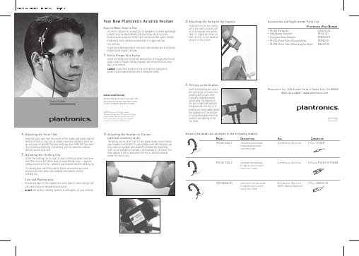
AviationHeadset6. Attaching the Headset to Glasses(optional mounting style)The spring clip on either side of the capsule allows you to installyour headset onto glasses. If your glasses have wire temples,youmay order an eyeglass bow adapter to thicken the mountingbase for the capsule and ensure a comfortable fit, as shown. Thebow adapter is not included with the MS50 aviation headset(order PN 10822-00).ODEL D ESCRIPTIONAviation headsets are available in the following models:MS50/T30-1 AMPLIFIED MICROPHONE(CARBON EQUIVALENT)FIVE-FOOT CORDMS50/T30-2AMPLIFIED MICROPHONE C OMMERCIAL A VIATION 2 P , PJ055 & PJ068(CARBON EQUIVALENT)FIVE-FOOT CORDSMS1066-01AMPLIFIED MICROPHONE(CARBON EQUIVALENT)FIVE-FOOT CORDAccessories and Replacement Parts ListP LANTRONICS P ART N UMBER• MS50 Eartip Kit 05091-00• Headband (double)18145-01• Eyeglass Bow Adapter 10822-00• MS50 Voice Tube (Round Amp) 18095-01• MS50 Voice Tube (Rectangular Amp) 83407-015. Adjusting the Clothing ClipAttach the clothing clip to a part of your clothing at about chest level.Press the ends of the cable clamp to allow enough slack — approxi-mately six inches (15cm)— between your headset and the clothing clip.Try moving your head from side to side to ensure that you haveallowed sufficient cable slack between the headset and theclothing clip.Care and Maintenance•Periodically wipe off the capsule and voice tube or boom using a softcloth which may be dampened with water.•Do Not use alcohol, cleaning solvents,or detergents on your headset.4. Adjusting the Voice TubePlace the voice tube near the corner of the mouth just below, but notdirectly in front of,your lips,as shown.Move the headband pivot barup and down to position the tube vertically, and rotate the tube itselffor horizontal positioning. If necessary, you can move the capsulelaterally on the pivot arm.49677-01 082911 08/29/11 Page 1New Plantronics Aviation HeadsetEasy to Uses guide carefully.whichever is latest.If you have a history of ear infections or allergies toyou should exercise care in using the eartip.49677-01 (08•11)Printed in U.S.A.Plantronics Inc., 345 Encinal Street / Santa Cruz, CA 95060(800) 544-4660 / 3. Putting on the HeadsetInsert the pivoting arm underthe spring clip, as shown. Thepivoting arm on which thecapsule is mounted allowsyou to wear the capsule onthe left or right side with theheadband over the top of, orbehind your head. Make certainthe capsule is on the outsideof the pivoting arm. Place theeartip in the opening of theear canal.2. Attaching the Eartip to the CapsuleSlide the end of the eartiponto the metal sound porton the capsule and gentlytwist it. Adjust the tube sothat it rests in the positionshown in the photo.。
汇承hc-05蓝牙模块用户手册(中文版)

HC-05蓝牙串口通信模块用户手册V2.1Rev22.1~2016/2/222016/2/22~2.0 2.1DRAWN BY:Ling Xin MODEL:HC-05(主从一体) CHECKED BY:Eric Huang描述:BC04外置8M Flash模块APPD.BY:SimonMokUART(默认)9600蓝牙模块HC-05、HC-06、HC-08无线模块HC-11、HC-12带底板模块参数架HC-USB-PPIN(默认)1234USB转TTL接口HC-05-USB、HC-06-USB HC-11-USBMODE(默认)从机新版模块带有蓝牙指示灯(靠近模块第1脚)。
模块的22脚LED_CON是指示灯控制脚,该脚接地,蓝牙指示灯关闭;该脚悬空,蓝牙指示灯亮。
如果要调整灯的亮度,可以在该脚接一个1K~47K的电阻到模块的31脚LED1,电阻越小,灯越亮。
贴片炉温参考建议首次大批量贴片生产的厂家,先过炉20~30片模块,检查炉温是否合适建议贴片锅炉炉温不得超过参考图温度,二次贴片降低5度左右,夏天可以再适当降低温度供电电压3.1~4.2V工作电流不大于50mA(以实测为准)尺寸大小27mm*13mm*2mm存储温度:-40℃至+85℃,工作温度:-25℃至+75℃数字2.4GHz无线收发射内置2.4GHz天线,用户无需调试天线蓝牙2.0,2Mbps空中波特率CSR BC04蓝牙芯片技术支持Android、WINXP、WIN7数据收发通过UART串口收发HC-05封装下载:/downloadDis.asp?id=15安卓串口助手APP下载:/downloadDis.asp?id=49 PC串口助手下载:/downloadDis.asp?id=44注:蓝牙模块的PIN2:UART-RXD不带上拉,如果单片机TXD无上拉能力的话需要在模块的UART-RXD脚上接个上拉电阻,这个很容易被用户忽略。
因为内容较长,请参考公司网站下载中心提供的文档HC-05AT指令集下载:/downloadDis.asp?id=64。
深圳市昇润科技HY-40R201低功耗蓝牙5.0模块规格书说明书

HY-40R201深圳昇润科技对本手册中可能出现的和/或规格书的权利,恕不另行通知用作生命支持设备或系统中的关键标是由美国蓝牙SIG公司所有.R201低功耗蓝牙 5.0模块规格书(40 pin)文档版本:V2.02017年10月25日深圳市昇润科技有限公司版权所有现的错误不承担责任。
此外,昇润科技保留随时行通知,并不承诺更新此处所包含的信息。
昇润的关键组件。
以及不承担各种专利或知识产权的.密级:公开资料留随时更改硬件,软件。
昇润的产品不被授权产权的授权使用;蓝牙商1.简述 (1)1-1应用: (1)1-2主要特征: (1)2. 产品型号 (2)2-1.(4 种天线形式可供选择)/( 可选: 带屏蔽罩或不带屏蔽罩) (2)2-2: HY-40R201PC机种屏蔽罩上FCC ID &( IC ID 待定义)印刷内容: (2)3. 模块尺寸与图片 (2)3.1 HY-40R201P / WMD40R201SR6P0 PCB IFA天线 (2)3-2.HY-40R201I /WMD40R201SR6I0 IPEX RF外接天线连接端子 (3)3-3. HY-40R201W / MD40R201SR6W0 金属线天线 (1/4波长偶极子天线) (3)3.4. HY-40R201C/ WMD40R201SR6C0 (陶瓷天线) (3)(4). 应用注意事项: (4)5.引脚分配和端口功能说明 (5)6. 电气特性 (6)6-1. 射频特性 及 电流功耗: (6)6-2. 绝对最大额定值 (7)6-3. ESD 额定值 (7)6-4.建议工作条件 (7)6-5.GPIO DC特性 (7)6-6. 时序要求 (8)6-7. 动作状态切换时序特性 (8)7. 模块方块图 (8)8.IC功能方块图 (9)9. 工作模式架构图 (9)10. 回流焊曲线建议 (无铅锡膏: Sn 96.5%, Ag 3%, Cu 0.5%) (10)11. HY-40R201PC / WMD40R201SR6PC 模块 FCC及 IC声明 (11)12.联系我们 (13)HY-40R201提供蓝牙低功耗特性:无线电,蓝牙协议栈,配置文件和客户应用程序的所需空间。
SCI FSB50650BS 高级动态SPM5系列描述说明书

FSB50650BSFSB50650B / FSB50650BS Motion SPM)5 SeriesDescriptionThe FSB50650B / FSB50650BS is an advanced Motion SPM 5 module providing a fully−featured, highperformance inverter output stage for AC Induction, BLDC and PMSM motors such as refrigerators, fans and pumps. These modules integrate optimized gate drive of the built−in MOSFETs (FRFET technology) to minimize EMI and losses, while also providing multiple on−module protection features including under−voltage lockouts and thermal monitoring. The built−in high−speed HVIC requires only a single supply voltage and translates the incoming logic−level gate inputs to the high−voltage, highcurrent drive signals required to properly drive the module’s internal MOSFETs. Separate open−source MOSFET terminals are available for each phase to support the widest variety of control algorithms.Features•UL Certified No. E209204 (UL1557)•Optimized for over 10 kHz Switching Frequency•500 V FRFET MOSFET 3−Phase Inverter with Gate Drivers and Protection•Built−In Bootstrap Diodes Simplify PCB Layout•Separate Open−Source Pins from Low−Side MOSFETs forThree−Phase Current−Sensing•Active−HIGH Interface, Works with 3.3 / 5 V Logic, Schmitt−trigger Input•Optimized for Low Electromagnetic Interference•HVIC Temperature−Sensing Built−In for Temperature Monitoring •HVIC for Gate Driving and Under−V oltage Protection •Isolation Rating: 1500 V rms/ min.•Moisture Sensitive Level (MSL)3 for SMD•These Devices are Pb−Free and are RoHS CompliantApplications•3−Phase Inverter Driver for Small Power AC Motor DrivesRelated Source•AN−9080 − FSB50450AS − User’s Guide for Motion SPM 5 Series •AN−9082 − Motion SPM5 Series Thermal Performance by Contact PressureSPM5E−023 / 23LD, PDD STDCASE MODEJSee detailed ordering and shipping information on page 2 of this data sheet.ORDERING INFORMATION$Y= ON Semiconductor Logo&Z= Assembly Plant Code&3= Data Code (Year & Week) &K= LotFSB50650X= Specific Device Code⇒ X = B or BSMARKING DIAGRAM$YFSB50650X&Z&K&E&E&E&3SPM5H−023 / 23LD, PDD STD,SPM23−BDCASE MODEMPACKAGE MARKING AND ORDERING INFORMATIONDevice Device Marking Package Packing Type Reel Size Quantity FSB50650B FSB50650B SPM5P−023Rail NA15FSB50650BS FSB50650BS SPM5Q−023Tape & Reel330 mm450ABSOLUTE MAXIMUM RATINGS (T C = 25°C, Unless otherwise noted)Symbol Parameter Conditions Rating Unit INVERTER PART(Each MOSFET Unless Otherwise Specified)V DSS Drain−Source Voltage of Each MOSFET500V *I D25Each MOSFET Drain Current, Continuous T C= 25°C 4.0A *I D80Each MOSFET Drain Current, Continuous T C= 80°C 2.5A *I DP Each MOSFET Drain Current, Peak T C= 25°C, PW < 100 m s10.3A *I DRMS Each MOSFET Drain Current, Rms T C= 80°C, F PWM< 20 kHz 1.8A rms CONTROL PART(Each HVIC Unless Otherwise Specified)V DD Control Supply Voltage Applied Between V DD and COM20V V BS High−side Bias Voltage Applied Between V B and V S20V V IN Input Signal Voltage Applied Between IN and COM−0.3 ~ V DD+0.3V BOOTSTRAP DIODE PART(Each Bootstrap Diode Unless Otherwise Specified.)V RRMB Maximum Repetitive Reverse Voltage500V * I FB Forward Current T C= 25°C0.5A * I FPB Forward Current (Peak)T C= 25°C, Under 1 ms Pulse Width 2.0A THERMAL RESISTANCEInverter MOSFET part, (Per Module) 2.1°C/W R th(j−c)Q Junction to Case Thermal Resistance(Note 1)TOTAL SYSTEMT J Operating Junction Temperature−40 ~ 150°C T STG Storage Temperature−40 ~ 125°C1500V rms V ISO Isolation Voltage60 Hz, Sinusoidal, 1 minute,Connection Pins to HeatsinkStresses exceeding those listed in the Maximum Ratings table may damage the device. If any of these limits are exceeded, device functionality should not be assumed, damage may occur and reliability may be affected.1.For the Measurement Point of Case Temperature T C, Please refer to Figure 4.2.Marking “ * ” Is Calculation Value or Design Factor.ing continuously under heavy loads or excessive assembly conditions (e.g. the application of high temperature/ current/ voltage and thesignificant change in temperature, etc.) may cause this product to decrease in the reliability significantly even if the operating conditions(i.e. operating temperature/ current/ voltage, etc.) are within the absolute maximum ratings and the operating ranges.PIN DESCRIPTIONPin No.Pin Name Pin Description1COM IC Common Supply Ground2V B(U)Bias Voltage for U Phase High Side FRFET Driving 3V DD(U)Bias Voltage for U Phase IC and Low Side FRFET Driving 4IN (UH)Signal Input for U Phase High −side 5IN (UL)Signal Input for U Phase Low −side 6N.C N.C7V B(V)Bias Voltage for V Phase High Side FRFET Driving 8V DD(V)Bias Voltage for V Phase IC and Low Side FRFET Driving 9IN (VH)Signal Input for V Phase High −side 10IN (VL)Signal Input for V Phase Low −side 11V TS Output for HVIC Temperature Sensing12V B(W)Bias Voltage for W Phase High Side FRFET Driving 13V DD(W)Bias Voltage for W Phase IC and Low Side FRFET Driving 14IN (WH)Signal Input for W Phase High −side 15IN (WL)Signal Input for W Phase Low −side 16N.C N.C17P Positive DC–Link Input18U, V S(U)Output for U Phase & Bias Voltage Ground for High Side FRFET Driving 19N U Negative DC–Link Input for U Phase 20N V Negative DC–Link Input for V Phase21V, V S(V)Output for V Phase & Bias Voltage Ground for High Side FRFET Driving 22N W Negative DC–Link Input for W Phase23W, V S(W)Output for W Phase & Bias Voltage Ground for High Side FRFET DrivingFigure 1. Pin Configuration and Internal Block Diagram (Bottom View)4.Source T erminal of Each Low −Side MOSFET is Not Connected to Supply Ground or Bias Voltage Ground Inside Motion SPM 5 product. External Connections Should be Made as Indicated in Figure 3.(1) COM (2) V (3) V (4) IN (5) IN (7) V (11) V (8) V (9) IN (10) IN (12) V (13) V (14) IN (15) IN (16) N.C(17) P(18) U, V S(U)(19) N U(20) N V (21) V, V S(V)(22) N W (23) W, V S(W)ELECTRICAL CHARACTERISTICS (T J = 25°C, V DD = V BS = 15 V Unless Otherwise Specified)Symbol Parameter Test Conditions Min.Typ.Max.Unit INVERTER PART (Each MOSFET Unless Otherwise Specified)BV DSS Drain−Source Breakdown Voltage V IN= 0 V, I D= 1 mA ( Note 5)500−−VI DSS Zero Gate Voltage Drain Current V IN= 0 V, V DS= 500 V−−1mA R DS(on)Static Drain−Source On−Resistance V DD= V BS= 15 V, V IN= 5 V, I D= 1.5 A− 1.43 1.8W V SD Drain−Source Diode Forward Voltage V DD= V BS= 15 V, V IN= 0 V, I D= −1.5 A−− 1.1Vt ON Switching Times V PN= 300 V, V DD= V BS= 15 V, I D= 1.5 AV IN= 0 V ↔5 V, Inductive Load L = 3 mH High−and Low−Side MOSFET Switching(Note 6)−440−nst OFF−580−ns t rr−100−nsE ON−30−m JE OFF−11−m J RBSOA Reverse−Bias Safe Operating Area V PN= 400 V, V DD= V BS= 15 V, I D= I DP,V DS= BV DSS, T J= 150°CHigh− and Low−Side MOSFET Switching (Note 7)Full Square CONTROL PART (Each HVIC Unless Otherwise Specified)I QDD Quiescent V DD Current V DD= 15 V, V IN= 0 V Applied Between V DD andCOM−−200m AI QBS Quiescent V BS Current V BS= 15 V, V IN= 0 V Applied BetweenV B(U)−U, V B(V)−V,V B(W)−W−−100m AI PDD Operating V DD Supply V DD− COM V DD = 15 V,f PWM = 20 kHz,Duty = 50%, Applied toOne PWM Signal Inputfor Low−Side−−900m AI PBS Operating V BS Supply Current V B(U)− V S(U), V B(V)− V S(V), V B(W)− V S(W)V DD = V BS = 15 V,f PWM= 20 kHz,Duty = 50%, Applied toOne PWM Signal Inputfor High−Side−−800m AUV DDD Low−Side Undervoltage Protection(Figure 8)V DD Undervoltage Protection Detection Level7.48.09.4VUV DDR V DD Undervoltage Protection Reset Level8.08.99.8VUV BSD High−Side Undervoltage Protection(Figure 9)V BS Undervoltage Protection Detection Level7.48.09.4VUV BSR V BS Undervoltage Protection Reset Level8.08.99.8V V TS HVIC Temperature sensing voltageoutputV DD= 15 V, T HVIC= 25°C (Note 8)600790980mVV IH ON Threshold Voltage Logic High Level Applied between IN andCOM −− 2.9VV IL OFF Threshold Voltage Logic Low Level0.8−−V BOOTSTRAP DIODE PART (Each Bootstrap Diode Unless Otherwise Specified)V FB Forward Voltage I F= 0.1 A, T C= 25°C (Note 9)− 2.5−V t rrB Reverse Recovery Time I F= 0.1 A, T C= 25°C−80−ns Product parametric performance is indicated in the Electrical Characteristics for the listed test conditions, unless otherwise noted. Product performance may not be indicated by the Electrical Characteristics if operated under different conditions.RECOMMENDED OPERATING CONDITIONSymbol ParameterConditionsMin.Typ.Max.Unit V PN Supply Voltage Applied between P and N −300400V V DD Control Supply Voltage Applied between V DD and COM 13.515.016.5V V BS High −Side Bias Voltage Applied between V B and V S 13.515.016.5V V IN(ON)Input ON Threshold Voltage Applied between V IN and COM3.0−V DD V V IN(OFF)Input OFF Threshold Voltage0−0.6V t dead Blanking Time for Preventing Arm −Short V DD = V BS = 13.5 ~ 16.5 V, T J ≤ 150°C 1.0−−m s f PWMPWM Switching FrequencyT J ≤ 150°C−15−kHz12347891011121314150.00.10.20.30.40.50.60.70.80.91.0Built in Bootstrap Diode V F −I F CharacteristicT C = 255CFigure 2. Built in Bootstrap Diode Characteristics (Typical)V F [V]56I F [A ]NOTES:5.BV DSS is the Absolute Maximum Voltage Rating Between Drain and Source T erminal of Each MOSFET Inside Motion SPM 5 product. V PNShould be Sufficiently Less Than This Value Considering the Effect of the Stray Inductance so that V DS Should Not Exceed BV DSS in Any Case.6.t ON and t OFF Include the Propagation Delay Time of the Internal Drive IC. Listed Values are Measured at the Laboratory T est Condition, and They Can be Different According to the Field Applications Due to the Effect of Different Printed Circuit Boards and Wirings. Please see Figure 6 for the Switching Time Definition with the Switching T est Circuit of Figure7.7.The peak current and voltage of each MOSFET during the switching operation should be included in the Safe Operating Area (SOA). Please see Figure 8 for the RBSOA test circuit that is same as the switching test circuit.8.V TS is only for sensing temperature of module and cannot shutdown MOSFET s automatically.9.Built in bootstrap diode includes around 15 W resistance characteristic. Please refer to Figure 1.HINLIN Output Note 00Z Both FRFET Off 010Low side FRFET On 10High side FRFET On11ForbiddenShoot through OpenOpenZSame as (0,0)These values depend on PWM control algorithmFigure 3. Recommended MCU Interface and Bootstrap Circuit with ParametersV DC 10.Parameters for bootstrap circuit elements are dependent on PWM algorithm. For 15 kHz of switching frequency, typical example of parameters is shown above.11.RC −coupling (R 5 and C 5) and C 4 at each input of Motion SPM 5 product and MCU (Indicated as Dotted Lines) may be used to prevent improper signal due to surge −noise.12.Bold lines should be short and thick in PCB pattern to have small stray inductance of circuit, which results in the reduction of surge −voltage.Bypass capacitors such as C 1, C 2 and C 3 should have good high −frequency characteristics to absorb high −frequency ripple −current.Figure 4. Case Temperature Measurement13.Attach the thermocouple on top of the heat −sink of SPM 5 package (between SPM 5 package and heatsink if applied) to get the correct temperature measurement.204060801001201401600.51.01.52.02.53.03.5T HVIC [°C]Figure 5. Temperature Profile of V TS (Typical)V T S [V ](a) Turn −on(b) Turn −offFigure 6. Switching Time DefinitionsFigure 7. Switching and RBSOA (Single −Pulse) Test Circuit (Low −side)C V V VInput Signal UV Protection StatusLow −side Supply, V MOSFET CurrentInput Signal UV ProtectionStatusHigh −side Supply, V MOSFET CurrentFigure 9. Under −Voltage Protection (High −Side)14.About pin position, refer to Figure 1.15.RC−coupling (R5and C5, R4and C6) and C4at each input of Motion SPM 5 product and MCU are useful to prevent improper inputsignal caused by surge−noise.16.The voltage−drop across R3affects the low−side switching performance and the bootstrap characteristics since it is placed betweenCOM and the source terminal of the low−side MOSFET. For this reason, the voltage−drop across R3should be less than 1 V in the steady−state.17.Ground−wires and output terminals, should be thick and short in order to avoid surge−voltage and malfunction of HVIC.18.All the filter capacitors should be connected close to Motion SPM 5 product, and they should have good characteristics for rejectinghigh−frequency ripple current.Figure 10. Example of Application CircuitPACKAGE DIMENSIONSSPM5H−023 / 23LD, PDD STD, SPM23−BD (Ver1.5) SMD TYPECASE MODEMISSUE O10SPM5E −023 / 23LD, PDD STD, FULL PACK, DIP TYPE CASE MODEJISSUE OSPM is a registered trademarks of Semiconductor Components Industries, LLC (SCILLC) or its subsidiaries in the United States and/or otherON Semiconductor and are trademarks of Semiconductor Components Industries, LLC dba ON Semiconductor or its subsidiaries in the United States and/or other countries.ON Semiconductor owns the rights to a number of patents, trademarks, copyrights, trade secrets, and other intellectual property. A listing of ON Semiconductor’s product/patent coverage may be accessed atON Semiconductor makes no warranty, representation or guarantee regarding the suitability of its products for any particular purpose, nor does ON Semiconductor assume any liability arising out of the application or use of any product or circuit, and specifically disclaims any and all liability, including without limitation special, consequential or incidental damages.PUBLICATION ORDERING INFORMATIONFSB50650BS。
HC-42蓝牙5.0BLE串口模块使用规格书
HC-42蓝牙5.0BLE串口模块用户手册目录一.模块介绍1.1特点简介 (3)1.2基本参数 (3)1.3电气特性 (3)1.4系列产品 (4)二.连接通讯说明2.1模块工作原理简单介绍 (4)2.2模块MCU等设备的连接通讯 (4)2.3模块与手机的连接通讯 (5)三.快速测试3.1参数架与模块连接 (5)3.2通讯测试 (5)四.开发利用4.1模块尺寸和引脚定义 (6)4.2嵌入方式 (7)4.3参考连接电路 (8)五.AT指令5.1模块参数设置AT指令 (9)5.2指令集总 (9)5.3指令说明 (10)六.关于汇承6.1公司简介 (14)发布日期:2018-02-081.1特点简介HC-42蓝牙串口通信模块是新一代的基于Bluetooth Specification V5.0BLE 蓝牙协议的数传模块。
无线工作频段为2.4GHz ISM ,调制方式是GFSK 。
模块最大发射功率为4dBm ,接收灵敏度-96dBm 。
模块大小26.9mm×13mm×2.0mm ,集成了邮票孔封装,可以贴片工艺,很方便嵌入应用系统之内。
1.2基本参数参数名称参数值参数名称参数值型号HC-42模块尺寸26.9X13mm 工作频段 2.4G 空中速率1Mbps/2Mbps 工作电压 1.8~3.6V 天线接口内置PCB 天线工作电流参照1.3表中所述停机电流0.3μA 通讯接口UART接收灵敏度-96dBm@1Mbps 通信电平 1.8~3.6V ,与工作电压一致工作湿度10%~90%发射功率-40~4dBm存储温度-40℃~+85℃参考距离40m/2Mbps (蓝牙5.0)工作温度-25℃~+75℃1.3电气特性数值备注电压特性1.8V~3.6V 若使用纽扣电池,必须保证电压在2.5V 以上参考电流(不包括LED )1.23mA/1.22mA全速广播/全速连接75μA/65uA 低功耗广播/低功耗连接(工作电流随广播间隔变化)0.3μA停机状态注:以上电流数据是基于气温25℃、工作电压3.3V 、出厂默认配置时测得,实际使用可能存在误差。
深圳云里物里科技股份有限公司蓝牙模块MS50SFA1说明书

股票代码:872374产品型号MODEL NO/DESCRIPTION产品名称蓝牙从模块产品型号MS50SFA1适用固件版本V2.4.x Version V1.0发布时间2020-05-26目录1. 产品概述 (3)2. 应用领域 (4)3. 模块尺寸图 (4)4. 电气参数 (5)5. 模块管脚图 (6)6. 引脚定义 (6)7. 模块使用操作说明 (8)8. 功耗参数 (17)9. PCB设计说明 (18)10. MCU参考代码 (19)11. 模块原理图 (22)12. 回流焊温度曲线图 (23)13. 支持设备 (23)14. 注意事项 (23)15. 包装信息 (24)16. 认证信息 (25)17. 质量保证 (25)附件:版本说明 (26)1.产品概述MS50SFA1串口从模块采用nRF52810 芯片,通过UART(串口)操作可以实现模块与手机(或其它主设备)之间数据传输。
本模块为从模块,有广播和连接状态,可通过命令设置和查看模块的广播名称,修改广播间隔和连接间隔等参数。
使用该模块用户可以快速把数据以蓝牙方式进行传输。
产品特点产品效果图MS50SFA(V1.x)PCB天线产品反面★ 远距离:10-60米(空旷环境);★ BLE协议栈深度优化,睡眠功耗1uA以下;★ 传输速率最快可达11kB/s;★ 支持供电电压检测;★ 支持串口指令配置;★ 支持 Android 4.3+,iOS7.0+;★ 无需 MFi;★ 通过BQB认证(证书编号QDID:138541);★ 带屏蔽罩。
(默认单位:mm 默认公差:±0.1)3.模块尺寸图2.应用领域该模块主要用于短距离的数据无线传输领域。
可以方便的和PC机的蓝牙设备相连,也可以与智能手机之间的数据互通。
避免繁琐的线缆连接,能直接替代串口线。
可广泛应用于智能家居、智能穿戴设备、消费电子、智慧医疗、安防设备、汽车设备、运动健身设备、仪器仪表、远程遥控等需要低功耗蓝牙系统的领域。
汇承HC-05蓝牙串口模块使用规格书(含指令集)

Rev 2
2.1
~2010/2/22
2016/2/22~
2.0
2.1
DRAWN BY:
XinLing
MODEL :
HC-05(主从一体)
CHECKED BY:
Chao Liang
描述:
BC04外置8M Flash模块
APPD. BY:
WenLei Mo
UART(默认)
三.连接通讯说明
3.1模块工作原理简单介绍………………………………………………………………………………………..............…………………………………5
3.2模块与MCU等设备的连接…………………………………………………………………………………………………………………………………5
3.3模块之间的连接通讯…………………………………………………………………………………………………….……………………………….....6
9600
蓝牙模块
HC-05、HC-06、HC-08、HC-31
无线模块
HC-11、HC-12
PIN(默认)
1234
带底板模块
参数架
HC-USB-P
HC-USB-T
MODE(默认)
从机
USB转TTL
HC-05-USB HC-06-USB
HC-08-USB
HC-11-USB
HC-12-USB
1.1为什么要用正品?
注③:输入脚,内部下拉。此脚接高电平,模块进入AT指令模式、主机用来清除已记录的从机地址。
5.2嵌入方式
模块天线部分下面不能敷铜,不能走线,否则影响信号,建议天线部分底板挖空,天线尽量靠近板边
Bluetooth 5.4 低功耗技术产品简介说明书
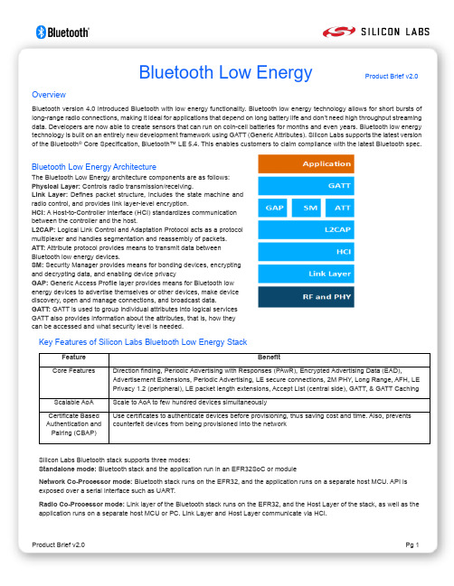
Bluetooth Low EnergyProduct Brief v2.0OverviewBluetooth version 4.0 introduced Bluetooth with low energy functionality. Bluetooth low energy technology allows for short bursts of long-range radio connections, making it ideal for applications that depend on long battery life and don’t need high throughput streaming data. Developers are now able to create sensors that can run on coin-cell batteries for months and even years. Bluetooth low energy technology is built on an entirely new development framework using GATT (Generic Attributes). Silicon Labs supports the latest version of the Bluetooth ® Core Specification, Bluetooth™ LE 5.4. This enables customers to claim compliance with the latest Bluetooth spec.Bluetooth Low Energy ArchitectureThe Bluetooth Low Energy architecture components are as follows: Physical Layer: Controls radio transmission/receiving.Link Layer: Defines packet structure, includes the state machine and radio control, and provides link layer-level encryption.HCI: A Host-to-Controller interface (HCI) standardizes communication between the controller and the host.L2CAP: Logical Link Control and Adaptation Protocol acts as a protocol multiplexer and handles segmentation and reassembly of packets. ATT: Attribute protocol provides means to transmit data between Bluetooth low energy devices.SM: Security Manager provides means for bonding devices, encrypting and decrypting data, and enabling device privacyGAP: Generic Access Profile layer provides means for Bluetooth low energy devices to advertise themselves or other devices, make device discovery, open and manage connections, and broadcast data.GATT: GATT is used to group individual attributes into logical services GATT also provides information about the attributes, that is, how they can be accessed and what security level is needed.Key Features of Silicon Labs Bluetooth Low Energy StackFeature BenefitCore FeaturesDirection finding, Periodic Advertising with Responses (PAwR), Encrypted Advertising Data (EAD),Advertisement Extensions, Periodic Advertising, LE secure connections, 2M PHY , Long Range, AFH, LE Privacy 1.2 (peripheral), LE packet length extensions, Accept List (central side), GATT, & GATT Caching Scalable AoA Scale to AoA to few hundred devices simultaneouslyCertificate Based Authentication and Pairing (CBAP) Use certificates to authenticate devices before provisioning, thus saving cost and time. Also, prevents counterfeit devices from being provisioned into the networkSilicon Labs Bluetooth stack supports three modes:Standalone mode: Bluetooth stack and the application run in an EFR32SoC or moduleNetwork Co-Processor mode: Bluetooth stack runs on the EFR32, and the application runs on a separate host MCU. API is exposed over a serial interface such as UART.Radio Co-Processor mode: Link layer of the Bluetooth stack runs on the EFR32, and the Host Layer of the stack, as well as the application runs on a separate host MCU or PC. Link Layer and Host Layer communicate via HCI.Technical ResourcesBluetooth Low Energy xG24 Technical Library Data Sheets, App Notes, and moreBluetooth Low Energy xG21 Technical Library Data Sheets, App Notes, and moreBluetooth Low Energy xG22 Technical Library Data Sheets, App Notes, and moreBluetooth Low Energy xG27 Data ShortBluetooth Low Energy API Documentation Bluetooth Low Energy API documentationSilicon Labs’ Bluetooth Low Energy HW supportHigh Performance device for Bluetooth LE and Bluetooth mesh applications thatrequire advance features and more Flash and RAMIndustry-leading, energyefficient device for Bluetooth LE applicationsOptimized for line-powered devices including LED bulbs, and gateways for Bluetooth LE and Bluetooth meshMost Battery Versatile SoC for Connected Health, Smart Home, Portable Products1536kB Flash 256kB RAM TX power 19.5dBm -105.7dBm @ 125kbps -97.6dBm @ 1Mbit/s -94.8dBm @ 2Mbit/s RX current 4.4mA @ 1MbpsTX current 5.0mA @ 0dBm1.3 µA Sleep current (16kB )Robust peripheral set AI/ML hardware accelerator Secure Vault High QFN40 5x5 (26) QFN48 6x6 (32)512kB Flash 32kB RAM TX power 6dBm -106.7dBm @ 125kbps -98.9dBm @ 1Mbit/s -96.2dBm @ 2Mbit/s RX current 3.6mA @ 1MbpsTX current 4.1mA @ 0dBm1.26µA Sleep current (16kB )Lowest Power Bluetooth LESecure Vault Mid QFN40 5x5 (26) QFN32 4x4 (18) TQFN32 4x4 (18)1024kB Flash 96kB RAM TX power 20dBm -104.9dBm @ 125kbps -97.5dBm @ 1Mbit/s -94.4dBm @ 2Mbit/s RX current 8.8mA @ 1MbpsTX current 9.3mA @ 0dBm+135 Junc. Temperature Secure Vault High Line-Powered Bluetooth LE QFN32 4x4 (20)768kB Flash 64kB RAM TX power 8dBm -106.9dBm @ 125kbps -99.2dBm @ 1Mbit/s -96.3dBm @ 2Mbit/s RX current 3.6mA @ 1Mbps TX current 4.1mA @ 0dBm 1.26µA Sleep current (16kB ) Secure Vault Mid QFN40 5x5 (26) QFN32 4x4 (18) TQFN32 4x4 (18)Bluetooth LE Target Applications• ESL • Medical• Direction Finding • Smart Home • Smart Tags • Sensors • Switches• Building Automation • HVACBluetooth LE Software / ToolsSilicon Labs Bluetooth Low Energy SDK helps you build smooth, reliable, and secure wireless connectivity for your IoT applications. Software and Tools features • Supports Bluetooth™ LE 5.4 • Wi-Fi Coexistence • Simplicity Studio IDE • GATT Configurator • Network Analyzer • Direction Finding Tool Suite • Bluetooth NCP Commander • Proprietary Radio Configurator • Energy Profiler • Tool Chain – GCC and IARLinks: Bluetooth Low Energy SDKLearning CenterReady for Bluetooth 5.4?Learn more about the latest specification Bluetooth Direction FindingBluetooth Location Services: AoA/AoD Why EFR?Silicon Labs EFR32 FeaturesSilicon Labs Secure Vault accreditations Product security certificationsBluetooth SoC and Module Selector Guide Bluetooth Low Energy Selector Guide Case Study: Rethinking Epilepsy Management EFR32 Portable Medical DeviceBluetooth BeaconsBluetooth Beacons and AdvertisingSilicon Labs’ Bluetooth LE Development KitsSilicon Labs’ Bluetooth development kits are divided into three categories based on your development need:• Rapid Prototyping • Proof of Concept• Advanced RF DevelopmentFor more information on the portfolio, check the link: https:///bluetooth-kitsBG22 BG21 BG24 BG27Disclaimer: Silicon Labs intends to provide customers with the latest, accurate, and in-depth documentation of all peripherals and modules available forsystem and software implementers using or intending to use the Silicon Labs products. Characterization data, available modules and peripherals, memory sizes and memory addresses refer to each specific device, and “Ty pical ” parameters provided can and do vary in different applications. Application examples described herein are for illustrative purposes only. Silicon Labs reserves the right to make changes without further notice to the product information, specifications, and descriptions herein, and does not give warranties as to the accuracy or completeness of the included information. Without prior notification, Silicon Labs may update product firmware during the manufacturing process for security or reliability reasons. Such changes will not alter the specifications or the performance of the product. Silicon Labs shall have no liability for the consequences of use of the information supplied in this document. This document does not imply or expressly grant any license to design or fabricate any integrated circuits. The products are not designed or authorized to be used within any FDA Class III devices, applications for which FDA premarket approval is required or Life Support Systems without the specific written consent of Silicon Labs. A “L ife Support System ” is any product or system intended to support or sustain life and/or health, which, if it fails, can be reasonably expected to result in significant personal injury or death. Silicon Labs products are not designed or authorized for military applications. Silicon Labs products shall under no circumstances be used in weapons of mass destruction including (but not limited to) nuclear, biological or chemical weapons, or missiles capable of delivering such weapons. Silicon Labs disclaims all express and implied warranties and shall not be responsible or liable for any injuries or damages related to use of a Silicon Labs product in such unauthorized applications. Note: This content may contain offensive terminology that is now obsolete. Silicon Labs is replacing these terms with inclusive language wherever possible. For more information, visit /about-us/inclusive-lexicon-projectTrademark InformationSilicon Laboratories Inc.®, Silicon Laboratories ®, Silicon Labs ®, SiLabs ® and the Silicon Labs logo ®, Bluegiga ®, Bluegiga Logo ®, EFM ®, EFM32®, EFR, Ember ®, Energy Micro, Energy Micro logo and combinations thereof, “the world ’s most energy friendly microcontroller s”, Redpine Signals ®, WiSeConnect , n-Link, ThreadArch ®, EZLink ®, EZRadio ®, EZRadioPRO ®, Gecko ®, Gecko OS, Gecko OS Studio, Precision32®, Simplicity Studio ®, Telegesis, the Telegesis Logo ®,USBXpress ®, Zentri, the Zentri logo and Zentri DMS, Z-Wave ®, and others are trademarks or registered trademarks of Silicon Labs. ARM, CORTEX, Cortex-M3 and THUMB are trademarks or registered trademarks of ARM Holdings. Keil is a registered trademark of ARM Limited. Wi-Fi is a registered trademark of the Wi-Fi Alliance. All other products or brand names mentioned herein are trademarks of their respective holders.Silicon Laboratories Inc. 400 West Cesar Chavez Austin, TX 78701IoT PortfolioQualitySupport & Community/products/quality/community。
- 1、下载文档前请自行甄别文档内容的完整性,平台不提供额外的编辑、内容补充、找答案等附加服务。
- 2、"仅部分预览"的文档,不可在线预览部分如存在完整性等问题,可反馈申请退款(可完整预览的文档不适用该条件!)。
- 3、如文档侵犯您的权益,请联系客服反馈,我们会尽快为您处理(人工客服工作时间:9:00-18:30)。
产
品规格书
PRODUCT SPECIFICATION
深圳云里物里科技股份有限公司
Version 2.4发布时间
2017-11-20
MODEL NO/DESCRIPTION 产品名称:蓝牙模块MS50SF5
产品型号:MS50SF5
版本说明
版本说明 (2)
1.概述 (4)
2.应用领域 (5)
3.机械尺寸(单位:mm) (5)
4.引脚定义 (6)
5.电气参数 (7)
6.支持的设备 (7)
7.包装信息 (8)
8.PCB设计说明 (8)
9.注意事项 (9)
10.质量保证 (9)
1.概述
MS50SF5是采用Nordic nRF52832设计的贴片蓝牙4.2模块。
它是一款高性价比、低功耗的片上系统(Soc)解决方案,适合蓝牙低功耗的应用,它降低了建立网络节点的成本。
它有一个ARM内核Cortex-M4F的RF收发器,MCU有更快的运行速度,内核运行速度达到64Mhz,它能够实现更强大的运算能力以及浮点运算的技术,能实现非常复杂的算法。
512KB FLASH程序空间、64KB RAM和其它功能强大的配套资源。
它适用于低功耗系统、超低的睡眠电流及运行时的低功耗。
正面反面
产品特征
蓝牙低功耗兼容技术
支持远程的应用
精确的接收信号强度检测(RSSI)
符合CE(欧洲)和FCC(美国)认证标准
内含高性能的ARM Cortex-M4F
带AES安全协议处理器
2.应用领域
※低功耗蓝牙系统
※移动配件
※运动和健身设备
※消费类电子
※人机接口设备
※健康和医疗
3.机械尺寸(单位:mm)
4.引脚定义
引脚符号引脚类型定义VDD Power Power supply
DCC Power DC/DC converter output pin GND Power Ground
ANT antenna antenna
SWDIO Digital I/O System reset(active low).Hardware debug and flash programming I/O
programming I/O.
SWCLK Digital
input Hardware debug and flash programming I/O
P0.04/
P0.09/P0.10/
P0.11/P0.12/
P0.17/P0.18/
P0.21/P0.27/
P0.28/P0.29/
P0.30/P0.30
Digital I/O General purpose I/O pin RST Digital I/O Configurable as system RESET pin
5.电气参数
参数数值备注
工作电压 1.8-3.6V DC
工作频率2400-2483MHz Programmable
频率误差+/-20KHz Null
发射功率-40~+4dBm Programmable
接收灵敏度-96dBm High gain mode
接收电流 5.4mA RX only run current(DCDC,3V)1Msps
发射电流7.5mA
Transmission power+4dBm,
RX only run current(DCDC,3V)1Msps 5.3mA Transmission power0dBm
睡眠功耗1uA以下Power mode3,connection-less state 遥控距离10-60米BER<0.1%,Open space
天线50ohm Null
模块尺寸16*12*2mm Null
传输距离10-60米半径距离
6.支持的设备
支持设备系统支持设备型号
iOS7.0及以上iPhone4S,iPhone5,iPhone5S,iphone6,iPhone6p,iPad3, iPad mini,iPad air等
Android4.3及以上华为,小米,OPPO,魅族,VIVO,Samsung Galaxy S III,HTC One等
7.包装信息
包装信息吸塑盘外箱
数量80个4000个
净重40克 4.5公斤
毛重75克9.5公斤
尺寸20x18x5cm32x23x40cm 8.PCB设计说明
9.注意事项
1、该芯片中有CMOS器件,在运输、使用过程中要注意防静电。
2、器件接地要良好,减少寄生电感。
3、尽量手工焊接,如需机贴,请控制回流焊温度不要超过205摄氏度。
4、模块天线下面不要铺铜。
5、天线应远离其他电路,防止辐射效率变低和影响其他电路正常使用。
6、模块放置应尽量远离其他低频电路,数字电路。
7、模块的接入电源建议使用磁珠进行隔离。
10.质量保证
工厂通过了ISO9001质量体系认证。
每一个产品都经过严格测试(发射功率测试、灵敏度测试、功耗测试,稳定性测试、老化测试等)。
声明:本规格书的内容仅供参考,如有更改,恕不另行通知。
云里物里科技对本规格书的内容有最终
解释权。