亿光光耦ELM600
亿光光耦ELM452
Revision :3 © 1 Copyright LifecyclePhase:
Date:2013-07-15 2010, Everlight All Rights Reserved. Release Date : May 13, 2013. Issue Release No: DPC-0000113 Rev.3 Expired Period: Forever
Revision :3 5 Copyright © LifecyclePhase:
2010, Everlight All Rights Reserved. Release Date : May 13, 2013. Issue No:DPC-0000113 Rev.3
Release Date:2013-07-15 14:59:03.0 Expired Period: Forever
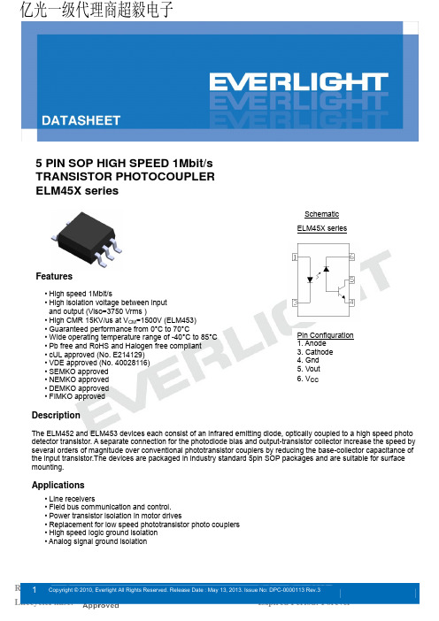
Pin Configuration 1. Anode 3. Cathode 4. Gnd 5. Vout 6. VCC
Description
The ELM452 and ELM453 devices each consist of an infrared emitting diode, optically coupled to a high speed photo detector transistor. A separate connection for the photodiode bias and output-transistor collector increase the speed by several orders of magnitude over conventional phototransistor couplers by reducing the base-collector capacitance of the input transistor.The devices are packaged in industry standard 5pin SOP packages and are suitable for surface mounting.
光耦600参数

光耦600参数光耦是由光电技术和电子技术相结合的器件,通常用于电气隔离和信号转换等领域。
光耦600是一种将光信号转换为电信号的型号,其参数如下:1. 光电耦合器(LED)参数:光通量为10mW,最大直流工作电流为50mA,最高正向电压为1.6V。
2. 光敏三极管(Phototransistor)参数:最大允许反向工作电压为25V,最大集电电流为50mA,最大功耗为150mW。
3. 共模传递比(CMR):CMR值为6000V/μs以上,为了保证光耦的隔离性能,CMR值应该尽可能大。
4. 工作温度范围:工作温度范围为-40℃至+85℃,在这个范围内保证正常工作。
5. 封装:光耦600通常采用双列直插封装,引脚间距为2.54mm,方便于PCB板上的安装和布局。
6. 光电耦合器(LED)和光敏三极管(Phototransistor)之间的耦合效率:光电耦合器和光敏三极管之间的耦合效率是光耦的重要指标之一,一般为30%到70%。
7. 响应时间:响应时间是指从光信号输入到输出电信号的时间,它主要取决于光电耦合器和光敏三极管的特性,一般在10μs到30μs之间。
8. 隔离电压:隔离电压是指光耦内部的LED和Phototransistor之间的电气隔离能力,一般应该大于1000V,以确保隔离效果的可靠性。
光耦600是一种性能优良的光耦器件,具有较高的隔离电压、共模传递比和耦合效率,可广泛应用于电气隔离和信号转换等领域。
光耦600的隔离性能非常好,具有较高的隔离电压,能够将输入端和输出端完全隔离开,避免了两个电路之间的相互干扰。
在工业控制、通讯等领域,光耦能够可靠地实现信号隔离,保证了电子设备的安全和稳定性。
光耦600的共模传递比(CMR)值很高,这也是衡量光耦隔离性能的重要指标之一。
CMR 值越高,表示光接收器和光发射器之间的隔离效果越好,能够对抗来自电力线、电场、磁场等噪声干扰的影响。
光耦600的响应时间较短,一般在10μs到30μs之间。
亿光光耦EL3023

6PIN DIP RANDOM-PHASE TRIAC DRIVER PHOTOCOUPLER EL301X, EL302X, EL305X SeriesFeatures:• Peak breakdown voltage -250V: EL301X -400V: EL302X -600V: EL305X• High isolation voltage between input and output (Viso=5000 V rms )• Compact dual-in-line package • Pb free and RoHS compliant.•UL and cUL approved(No. E214129)• VDE approved (No.132249)• SEMKO approved • NEMKO approved • DEMKO approved •FIMKO approvedDescriptionThe EL301X, EL302X and EL305X series of devices each consist of a GaAs infrared emitting diode optically coupled to a monolithic silicon random phase photo Triac.They are designed for interfacing between electronic controls and power triacs to control resistive and inductive loads for 115 to 240 VAC operations.Applications●Solenoid/valve controls ●Lamp ballasts●Static AC power switch●Interfacing microprocessors to 115 to 240Vac peripherals ●Incandescent lamp dimmers ●Temperature controls ●Motor controlsSchematic126543Pin Configuration 1. Anode 2. Cathode3. No Connection4. Terminal5. Substrate(do not connect)6. Terminal亿光一级代理商超毅电子Absolute Maximum Ratings (Ta=25 )Parameter Symbol Rating Unit Input Forward current I F60mA Reverse voltage V R6VPower dissipationDerating factor (above T a = 85 C)P D100mW3.8mW/°COutputOff-state OutputTerminal Voltage EL301XV DRM250V EL302X400EL305X600Peak Repetitive Surge Current(pw=100μs,120pps)I TSM1A On-State RMS Current I T(RMS)100mAPower dissipationDerating factor (above T a = 85 C)P C300mW7.4mW/Total power dissipation P TOT330mW Isolation voltage*1V ISO5000Vrms Operating temperature T OPR-55 to 100 Storage temperature T STG-55 to 125 Soldering Temperature*2T SOL260 Notes:*1AC for 1 minute, R.H.= 40 ~ 60% R.H. In this test, pins 1, 2&3are shorted together, and pins4, 5 & 6are shorted together. *2 For 10 secondsElectro-Optical Characteristics (Ta=25 unless specified otherwise)InputParameter Symbol Min.Typ.*Max.Unit Condition Forward Voltage V F- 1.18 1.5V I F=10mA Reverse Leakage current I R--10µA V R=6V OutputParameter Symbol Min.Typ.*Max.Unit ConditionPeak Blocking Current I DRM--100nA V DRM = Rated V DRM I F=0mAPeak On-state Voltage V TM-- 2.5V I TM=100mA peak, I F=Rated I FTCritical Rate of Rise off-state Voltage EL301XEL302X dv/dt-100-V/µsV PEAK=Rated V DRM,I F=0 (Fig. 8)EL305X1000--V PEAK=400V,I F=0 (Fig. 8)Transfer CharacteristicsParameter Symbol Min.Typ.*Max.Unit ConditionLED Trigger Current EL3020I FT30mA Main terminal Voltage=3V EL3010EL3021EL3051--15EL3011EL3022EL3052--10EL3012EL3023EL3053--5Holding Current I H-250-µA * Typical values at T a= 25°CTypical Electro-Optical Characteristics CurvesFigure 8. Static dv/dt Test Circuit & WaveformMeasurement MethodThe high voltage pulse is set to the required V PEAK value and applied to the D.U.T. output side through the RC circuit above. LED current is not applied. The waveform V T is monitored using a x100 scope probe. By varying R TEST , the dv/dt (slope) is increased, until the D.U.T. is observed to trigger (waveform collapses). The dv/dt is then decreased until the D.U.T. stops triggering. At this point, τRC is recorded and the dv/dt calculated.For example, V PEAK = 400V for EL302X series. The dv/dt value is calculated as follows:V PEAKApplied V T WaveformτRC0.632 x V PEAK50 Ω10 k ΩD.U.T.R TESTHigh Voltage Pulse SourceC TESTV T A KT1T20.63 x 400τRCdv/dt = = 252τRC0.632 x V PEAK τRCdv/dt =Order InformationPart NumberEL301XY(Z)-Vor EL302XY(Z)-Vor EL305XY(Z)-VNoteX = Part No. for EL301x (0, 1 or 2)X = Part No. for EL302x, EL305x (1, 2 or 3)Y = Lead form option (S, S1, M or none)Z = Tape and reel option (TA, TB or none).V = VDE safety approved (optional)Option Description Packing quantity None Standard DIP-665 units per tube M Wide lead bend (0.4 inch spacing)65 units per tube S Surface mount lead form65 units per tube S(TA)Surface mount lead form + TA tape & reel option1000 units per reel S (TB)Surface mount lead form + TB tape & reel option1000 units per reel S1 (TA)Surface mount lead form (low profile) + TA tape & reel option1000 units per reel S1 (TB)Surface mount lead form (low profile) + TB tape & reel option1000 units per reelPackage Dimension(Dimensions in mm) Standard DIP TypeOption M TypeOption S TypeOption S1 TypeRecommended pad layout for surface mount leadformDevice MarkingNotesEL denotes EVERLIGHT3053 denotes Device NumberY denotes 1 digit Year codeWW denotes 2 digit Week codeVdenotes VDE (optional)EL3053YWWVTape dimensionsDimension No.A B Do D1E F Dimension (mm)10.4±0.17.5±0.1 1.5±0.1 1.5+0.1/-01.75±0.17.5±0.1Dimension No.Po P1P2t W K Dimension (mm)4.0±0.1512±0.12.0±0.10.35±0.0316.0±0.24.5±0.1Revision : 7Release Date:2014-09-24 17:43:02.011Copyright © 2010, Everlight All Rights Reserved.Release Date:September 3, 2014. Issue No:DPC-0000059 Rev.7Precautions for Use1. Soldering Condition1.1 (A) Maximum Body Case Temperature Profile for evaluation of Reflow ProfileNote: Reference: IPC/JEDEC J-STD-020DPreheatTemperature min (T smin ) 150 °C Temperature max (T smax )200°CTime (T smin to T smax ) (t s )60-120 seconds Average ramp-up rate (T smax to T p ) 3 °C/second maxOtherLiquidus Temperature (T L )217 °C Time above Liquidus Temperature (t L )60-100 sec Peak Temperature (T P )260°C Time within 5 °C of Actual Peak Temperature: T P -5°C 30 sRamp-Down Rate from Peak Temperature 6°C /second max.Time 25°C to peak temperature 8 minutes max.Reflow times 3 times .Revision : 7Release Date:2014-09-24 17:43:02.012 2010, Everlight All Rights Reserved.Release Date:September 3, 2014. Issue No:DPC-0000059 Rev.70 DISCLAIMER1.Above specification may be changed without notice. EVERLIGHT will reserve authority on material change for abovespecification.2.When using this product, please observe the absolute maximum ratings and the instructions for using outlined in thesespecification sheets. EVERLIGHT assumes no responsibility for any damage resulting from use of the product which does not comply with the absolute maximum ratings and the instructions included in these specification sheets.3.These specification sheets include materials protected under copyright of EVERLIGHT corporation. Please don’treproduce or cause anyone to reproduce them without EVERLIGHT’s consent.。
AEM ES0603V014CT-spec

Production Specification产 品 规 格 书Product Name : GcDiode TM ESD SuppressorsAEM Part Number :ES0603V014CTAEM Components (Suzhou) Co., Ltd.458 Shenhu Road, Suzhou Industrial ParkJiangsu, P.R. China, 215122TEL: 86-512-6258-0028FAX: 86-512-6258-0018* The specification is the property of AEM Components (Suzhou) Co., Ltd. and shall not be copied or used for commercial purposes without permission.1 Operating Temperature Range-55℃ ~ +125℃2 Electrical Characteristics30 V (typical) (measured per IEC61000-4-2, Level 4, 8 kV)Less than 1ns Response Time Characteristic ValueESD CapabilityIEC61000-4-2 Direct Discharge 300 V (typical) (measured per IEC61000-4-2, Level 4, 8 kV)Production SpecificationAEM Part Number:Trigger Voltage Clamping Voltage ES0603V014CTGcDiode TMESD SuppressorsIEC61000-4-2 Air Discharge Level 4 - 8 kV Level 4 - 15 kV3 Shape and Dimensions: Inch (mm)Less than 1 ns Response Time 0.063 ± 0.0060.031 ± 0.0060.031 ± 0.0060603 (1608)0.25 pF (typical)0.1 nA (typical), (measured at 14 VDC)14 VDC (max.) Leakage Current Capacitance (1.0 GHz) BW L W Rated Voltage ESD Pulse Withstand1000 Pulses (typical)T (1.60 ± 0.15)(0.80 ± 0.15)(0.80 ± 0.15)(0.36 ± 0.15)Size 0.014 ± 0.006()()()()Production SpecificationGcDiode TM ESD SuppressorsAEM Part Number: ES0603V014CT4 Representative test waveform per IEC61000-4-2 Level 4, 8 kVProdcution SpecificationGcDiode TM ESD SuppressorsAEM Part Number: ES0603V014CT5 Product IdentificationES 0603 V014 C T(1) (2) (3) (4) (5)(1) Category code(2) Dimension code: L x W (inch)The first two digits - L (length)The last two digits - W (width)(3) Rated voltage code: V014 - 14 VDC(4) Series code(5) Package code:T - Tape & ReelB - Bulk6 Features6.1Excellent protection against ESD damage6.2Ultra low capacitance for high speed data lines6.3Very low leakage current6.4Instant response time (<1 ns)6.5Bi-directional flip-chip design6.6Glass ceramic monolithic structure with special Ag/Pd composite ESD materials6.7Silver termination with nickel and lead-free solder platingoffering excellent solderability and leach resistance6.8Outstanding durability (able to withstand 1000 strikes typical)6.9100 % lead-free6.10RoHS compliant7 Typical Applications7.1 USB7.2 IEEE13947.3 HDMI7.4 DisplayPort7.5 DVI7.6 Antennas7.7 UDI7.8 E-SATA7.9 LCD TV7.10 Set Top Box7.11 DVD7.12 LCD Monitor7.13 Notebook7.14 Mobile Phone7.15 Netbook7.16 MID8 Recommended PCB oard Land Pattern9 Recommended Temperature Profile for Reflow SolderingInch (mm)Inch (mm)0.031 (0.80)0.039 (1.00)G H Inch (mm)GcDiode TM ESD SuppressorsChip Size L AEM Part Number:ES0603V014CT0603 (1608)0.087 (2.20)10 Special Measuring Equipment 10CapacitanceCapacitance is measured with an Agilent LCR meter.11 Reliability TestsFlexure StrengthSolderability Soldering Heat ResistanceThermal ShockMechanical VibrationMechanical Shock Salt Spray Moisture Resistance Endurance 85 ± 2 ℃,1000 +48/-0 hr, rated voltage100 cycles between -65℃ and +125℃ ; Per MIL-STD-202Method 10710 cycles, Per Mil-STD-202 Method 1060.4 ”D.A. or 30 G between 5-3000 Hz; Per MIL-STD-202Method 2041500 G, 0.5 ms, half-sine shocksTest Conditions&Reference255℃, 5 seconds; Per MIL-STD-202 Method 2082 mm Bend; Per IEC68-2-2148 hour exposure; Per MIL-STD-202 Method 101GcDiode TM ESD SuppressorsOne dip at 260℃ for 60 seconds. Per MIL-STD-202Method 210AEM Part Number:Test itemES0603V014CT12 Packaging12.1Surface mount ESD suppressors are provided on tape-and-reel for use in pick-and-placemachines or in bulk for special applications. Both tape-and-reel and bulk products are sealed in plastic bags with desiccant. The reel size is 7 inches. 12.2Tape Dimensions: Inch (mm)(2.00 ± 0.05)0.079 ± 0.002(1.60+0.10)0.059+0.0040.157 ± 0.0040.315 ± 0.0040.069 ± 0.0040.138 ± 0.002(3.50 ± 0.05)P 1D 0D 1(1.75 ± 0.10)N/A0.157 ± 0.004(4.00 ± 0.10)(4.00 ± 0.10)(8.00 ± 0.10)P 0P 2E 1F W AEM Part Number:ES0603V014CTSize0603(1608)A 0B 0(1.80 ± 0.10)(0.60 ± 0.08)0.039 ± 0.0040.071 ± 0.004Production SpecificationGcDiode TM ESD SuppressorsK 0TypePaper0.024 ± 0.003(1.00 ± 0.10)12.3 Quantity Per Reel13 Storage13.1 The maximum ambient temperature shall not exceed 35℃.Storage temperature higher than 35℃ could result in the deformation of packaging materials.13.2The maximum relative humidity recommended for storage is 75 %.High humidity with high temperature could accelerate the oxidation of the solder plating on the termination and reduce the solderability of the components.The insulation resistance of the ESD suppressorscould be reduced if the products are stored in a high humidity environment.13.3Sealed plastic bags with desiccant shall be used to reducethe oxidation of the termination and shall only be opened prior to use.13.4The products shall not be stored in areas where harmful gasescontaining sulfur or chlorine are present.0603 (1608)4,000Production SpecificationGcDiode TM ESD Suppressors7 inch (178 mm) ReelAEM Part Number: ES0603V014CTChip Size Parts on。
亿光光藕EL817规格书
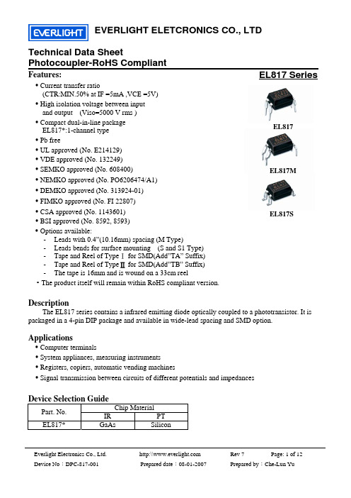
Photocoupler-RoHS Compliant EL817 SeriesFeatures: • Current transfer ratio(CTR:MIN.50% at IF =5mA ,VCE =5V) • High isolation voltage between input and output (Viso=5000 V rms ) • Compact dual-in-line package EL817*:1-channel type • Pb free• UL approved (No. E214129) • VDE approved (No. 132249) • SEMKO approved (No. 608400)• NEMKO approved (No. PO6206474/A1) • DEMKO approved (No. 313924-01)• FIMKO approved (No. FI 22807) • CSA approved (No. 1143601) • BSI approved (No. 8592, 8593) • Options available:- Leads with 0.4”(10.16mm) spacing (M Type)- Leads bends for surface mounting (S and S1 Type) - Tape and Reel of Type for SMD(Add”TA” Suffix)Ⅰ - Tape and Reel of Type Ⅱfor SMD(Add”TB” Suffix) - The tape is 16mm and is wound on a 33cm reel• The product itself will remain within RoHS compliant version.DescriptionThe EL817 series contains a infrared emitting diode optically coupled to a phototransistor. It is packaged in a 4-pin DIP package and available in wide-lead spacing and SMD option.Applications• Computer terminals• System appliances, measuring instruments• Registers, copiers, automatic vending machines• Signal transmission between circuits of different potentials and impedancesDevice Selection GuideChip MaterialPart. No.IR PTEL817* GaAs SiliconEL817EL817SEL817MPhotocoupler-RoHS CompliantEL817 SeriesPhotocoupler-RoHS CompliantEL817 SeriesS1 TypeNotes:1.Rank shall be or shall not be marked2.Factory code shall be marked (T: Taiwan / C: China)3.Year date code4.2-digit work week5.All dimensions are in millimeters6.Specifications are subject to change without noticePhotocoupler-RoHS Compliant EL817 SeriesAbsolute Maximum Ratings ( Ta=25°C )Parameter Symbol Rating UnitForward Current I F 50 mAPeak Forward Current*1I FM 1 A Input Reverse VoltageV R 6 V Power Dissipation P 70 mWCollector Power DissipationP C 150 mW Output Collector CurrentI C 50mA Collector-Emitter Voltage V CEO 35 V Emitter-Collector Voltage V ECO 6V Total Power DissipationPtot 200 mW *2Isolation Voltage Viso 5000 V rms Operating TemperatureTopr -55~+110 °C Storage TemperatureTstg -55~+125 °C *3Soldering TemperatureTsol260°C*1Frequency=100 HZ ,10uS Duty*2AC for 1 minute, R.H= 40~ 60%RH-Isolation voltage shall be measured using the following method. (1) Short between anode and cathode on the primary side and between collector, emitter and base on the secondary side.(2) The isolation voltage tester with zero-cross circuit shall be used. (3) The waveform of applied voltage shall be a sine wave*3For 10 secondsPhotocoupler-RoHS Compliant EL817 SeriesElectro-Optical Characteristics (Ta=25°C)Parameter Symbol Min. Typ. Max. Unit ConditionForward V F - 1.2 1.4 V I F =20mA Peak ForwardCurrent V FM 3.0 V I FM =0.5A Reverse Current I R - - 10 uAV R =4VInputTerminal Ct - 30 250 pF V=0,f=1kHz Collector Dark currentI CEO - - 100 nAV CE =20VOutputCollector- Emitter breakdown voltage BV CEO 35 - - V Ic=0.1mACurrent Transfer ratio CTR 50-600 % I F =5mA ,V CE =5VCollector- Emitter saturation voltageV CE(sat) - 0.1 0.2 V I F =20mA ,Ic=1 mAIsolation resistance R ISO 5×10¹⁰ 1011 - ΩDC500V,40~60%R.HFlotation capacitance Cf - 0.6 1.0 pF V=0, f=1MHz Cut-off frequency fc - 80 - kHz V CE =5V, I C =2 mAR L =100Ω, -3dBRise time t r - 4 18 us Transfer CharacteristicsFall timet f - 3 18 usV CE =2VI C =2mA,R L =100ΩPhotocoupler-RoHS CompliantEL817 Series SupplementCurrent Transfer Ratio CTRSub-Model No. Rank mark CTR (%) ConditionEL817* note 1 50 to 600EL817* (L) note2L 50 to 100EL817* (A) A 80 to 160EL817* (B) B 130 to 260 EL817* (C) C 200 to 400 EL817* (D) D 300 to 600 EL817* (AB) A or B 80 to 260 EL817* (BC) B or C 130 to 400 EL817* (CD) C or D 200 to 600 I F = 5 mA V CE = 5 V T a = 25°CNote1. The symbol “ * “ can be none or S or M by different leads form request Note2. The symbol “ ( ) ” can be CTR rankPhotocoupler-RoHS CompliantEL817 Series RELIABILITY PLANz The reliability of products shall be satisfied with items listed below.Confidence level : 90 % , LTPD : 10 %Classification Test Item Description & Condition (Acc.)Sample FailureCriteriaReferenceStandardOperation Life * Ta = 25±3°CIR: If = 50 mAPt: Pc = 130 mW ( Vf=1.4v) , 1000 hrs 0 / 22 MIL-S-750 : 1026MIL-S-883 : 1005JIS C 7021 : B-1High Temperature / High Humidity Reverse Bias (H3TRB) Ta = 85 ±3°C , Humi. = 85 % rhPt: 80% * Vce (max rating) , 1000 hrs0 / 22 JIS C 7021 : B-11High Temperature Reverse Bias (HTRB) Ta = 105 ±3°CPt: 100% * Vce (Max rating) ,1000 hrs0 / 22 JIS C 7021 : B-8Low Temperature Storage Ta = -50 ±3°C , 1000 hrs 0 / 22 JIS C 7021 : B-12High Temperature Storage Ta = 125 ±3°C , 1000 hrs 0 / 22 JIS C 7021 : B-10MIL-S-883 : 1008 Endurance testAuto clave P = 15 PSIG , Ta = 121 °C ,Humi. = 100 % rh , 48 hrs0 / 22 JESD 22-A102-BTemperature Cycling (Air to Air) 125°C ~ - 55 °C30 ~ 30 min , 100 cycles0 / 22 MIL-S-883 :1010JIS C 7021 : A-4Thermal Shock (Liquid to Liquid) 125 ~ - 55°Ct (dwell) = 5 mint (trans.) = 10 sec , 100 cycles0 / 22 MIL-S-202 : 107DMIL-S-750 : 1051MIL-S-883 :1011Solder Resistance Ta = 260 ±3°Ct (dwell) = 10 ±1 sec 0 / 22 MIL-S-750 : 2031JIS C 7021 : A-1Environmental TestSolder Ability Ta = 230 ±3 °Ct (dwell) = 5 ±1 sec 0 / 22CTR shift > 1.2Vf > U* 1.0Ir > U * 1.0Vce(sat) >U*1.0Bvceo < L*1.0Bveco < L*1.0L :LowSpec.LimitU : Up Spec.LimitMIL-S-883 : 2003JIS C 7021 : A-2Photocoupler-RoHS CompliantEL817 Seriesz Packing Quantity1.100 Pcs/ Per Tube2.25 Tubes / Inner Carton3.12 Inner Cartons / Outside Carton3. Outside Carton。
亿光光耦EL814

09:38:06.0
亿光一级代理商超毅电子
DATASHEET 4 PIN DIP PHOTOTRANSISTOR PHOTOCOUPLER AC INPUT PHOTOCOUPLER EL814 Series
Electro-Optical Characteristics (Ta=25
unless specified otherwise)
Input
Parameter Forward Voltage Input capacitance Symbol VF Cin Min. Typ. 1.2 50 Max. 1.4 250 Unit V pF Condition IF = ± 20mA V = 0, f = 1KHz
Output
Parameter Collector-Emitter dark current Collector-Emitter breakdown voltage Emitter-Collector breakdown voltage Symbol ICEO BVCEO BVECO Min 80 6 Typ. Max. 100 Unit nA V V Condition VCE = 20V, IF = 0mA IC = 0.1mA IE = 0.1mA
Transfer Characteristics
Parameter Current Transfer ratio EL814 CTR EL814A 50 0.7 VCE(sat) RIO fc CIO Tr Tf 5×10 10
Symbol
Min 20
Typ. -
Max. 300
Unit
Condition
Option None M S (TA) S (TB) S1 (TA) S1 (TB) S (TU) S (TD) S1 (TU) S1 (TD) Standard DIP-4
光耦的应用
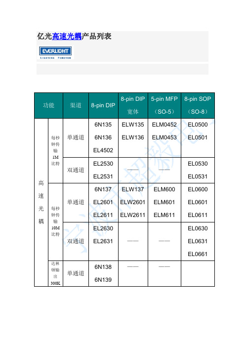
功能渠道8-pin DIP8-pin DIP宽体5-pin MFP(SO-5)8-pin SOP(SO-8)高速光耦每秒钟传输1M比特单通道6N1356N136EL4502ELW135ELW136ELM0452ELM0453EL0500EL0501 双通道EL2530EL2531————EL0530EL0531每秒钟传输10M比特单通道6N137EL2601EL2611ELW137ELW2601ELW2611ELM600ELM601ELM611EL0600EL0601EL0611 双通道EL2630EL2631 ————EL0630EL0631EL0661 达林顿输出300K单通道6N1386N139————亿光的高速光耦一般应用在电源上,具体应用在放点等离子,固态继电器,工业测量机,调制器,电话,空调控制板,可编程逻辑控制器等等。
电源工作渠道固态继电器(SSR)Photo TriacEL302X,EL305X,EL304X,EL306X,EL308XELM302X,ELM305X,ELM304X,ELM306X,ELM308X高速光耦应用在空调标准EL817,EL357N-G 空调机应用到的光耦驱动EL3120高速光耦应用在驱动电源标准EL357N-G,EL3H7-G 驱动器应用到的光耦高速6N136,EL0500高速光耦的应用末端设备电话交换系统so8封装晶体管末端设备电机驱动逆变器/伺服系统栅极驱动器末端设备仪表控制/工业网络缝纫机串行总线接口隔离建议的使用设备:8-Pin DIP:6N135,6N136,,EL2503 8-Pin SOP:EL0500,EL0501总线网络描述·总线接口隔离·隔离控制器和分析设备(I/O,,伺服电机,控制板,流出物处理元件)应用·工厂自动化网络(总线接口,总线,CC-LINK)建议的使用设备:5-pin SOP:ELMO452,ELMO4538-pin DIP:EL2502,EL25038-pin SOP:EL0500,EL0501数据传输框图应用:·RS485和RS-422 的隔离接口·I²C的隔离接口建议的使用设备:5-pin SOP:ELM600,ELMO601,ELM06118-pin DIP:EL2601,EL26118-pin SOP:EL0500,EL0501,EL0601,EL0611PLC输入/输出(可编程逻辑控制器)通讯(面板与面板之间)建议的使用设备:5-pin SOP:ELM601,ELM6118-pin SOP:EL0601,EL0611,EL0630,EL0631电机控制描述·电流隔离电机线和控制集成电路·电机驱动控制的高速开关应用·IPM驱动/变频驱动建议的使用设备:5-pin SOP:ELM452,ELM453 8-pin DIP:EL0452,EL0453 8-pin SOP:EL0452,EL0453筑控设备描述:·通信线路之间的隔离室控制器·电机驱动控制的高速开关应用:·数据通信·IPM驱动/变频驱动建议的使用设备:5-pin SOP:ELM452,ELM4538-pin SOP:EL0630,EL0631,EL0611。
亿光的光耦el817的工作寿命评估方式

亿光的光耦el817的工作寿命评估方式光耦是一种将输入光信号和输出电信号进行电光转换的器件,广泛应用于各种电子设备中。
其中,亿光的光耦型号el817是一种常用的光耦产品。
在评估el817的工作寿命时,可以考虑以下几个方面:光电转换性能、环境因素、温度、电器荷电量、加电击波和终端压力。
首先,光电转换性能是评估el817工作寿命的重要指标之一。
光电转换性能包括光耦的转换速度、滞后时间和线性度等方面。
在实际应用中,光耦的转换速度要求越高,生命周期就越短。
因此,使用el817作为光耦时,需要根据具体需求选择合适的型号,并根据其提供的转换速度等参数进行评估。
其次,环境因素也会对el817的工作寿命产生影响。
环境因素主要包括湿度、光照强度和尘埃等。
湿度过高会导致光耦内部元件的腐蚀,从而降低工作寿命;光照强度过高会导致光耦内部元件的老化,同样会缩短工作寿命;而尘埃对光耦的外部结构形成阻隔,影响光信号的输入和输出,进而影响光耦的转换性能和工作寿命。
此外,温度对el817的工作寿命也有重要影响。
温度过高会使光耦内部元件的粘结材料老化,导致光电转换性能下降,从而缩短工作寿命。
因此,在设计电路时,需要根据实际环境温度,选择合适的散热措施,以保证el817在合适的温度范围内工作。
同时,电器荷电量也是评估el817工作寿命的重要因素之一。
电器荷电量是指光耦元器件上积累的电荷量,过高的电器荷电量会导致静电放电现象,进而对光电转换性能和工作寿命造成不可逆的损害。
此外,加电击波也是一个重要的评估因素。
在实际应用中,电路开关和继电器的加电冲击会影响光耦的工作寿命。
因此,在电路设计中,需要考虑合适的保护电路来减小电路开关对光耦产生的冲击,从而提高工作寿命。
最后,终端压力也是影响el817工作寿命的因素之一。
终端压力过大,会使光耦内部元件的结构变形,进而影响光电转换性能和工作寿命。
因此,在应用中需要注意处理好终端压力,避免对光耦造成不可逆的损害。
- 1、下载文档前请自行甄别文档内容的完整性,平台不提供额外的编辑、内容补充、找答案等附加服务。
- 2、"仅部分预览"的文档,不可在线预览部分如存在完整性等问题,可反馈申请退款(可完整预览的文档不适用该条件!)。
- 3、如文档侵犯您的权益,请联系客服反馈,我们会尽快为您处理(人工客服工作时间:9:00-18:30)。
5 PIN SOP HIGH SPEED10MBit/s LOGIC GATE PHOTOCOUPLER ELM6XX seriesFeatures•Compliance Halogen Free .(Br <900 ppm ,Cl <900 ppm , Br+Cl < 1500 ppm)• High speed 10Mbit/s• Guaranteed performance from -40 to 85 • Logic gate output• High isolation voltage between input and output (Viso=3750 V rms )•Compliance with EU REACH • Pb free and RoHS compliant.•UL and cUL approved(No. E214129)• VDE approved (No. 40028116)• SEMKO approved • NEMKO approved • DEMKO approved • FIMKO approvedDescriptionThe ELM600, ELM601 and ELM611 are consists of an infrared emitting diode optically coupled to a high speed integrated photo detector logic gate with a strobable output.The devices are packaged in a 5-pin small outline package which conforms to the standard footprint.Applications Truth Table• Ground loop elimination• LSTTL to TTL, LSTTL or 5 volt CMOS •Line receiver, data transmission • Data multiplexing• Switching power supplies•Pulse transformer replacement •Computer peripheral interfaceInputOutput H L LHSchematicPin Configuration 1, Anode 3, Cathode 4, Gnd 5, Vout 6, V CCAbsolute Maximum Ratings (T A=25o C)Parameter Symbol Rating UnitInputForward current I F50mA Reverse voltage V R5V Power dissipation P D100mWOutput Power dissipation P C85mW Output current I O50mA Output voltage V O7.0V Supply voltage V CC7.0VOutput Power Dissipation P O85mW Isolation Voltage*1V ISO3750V rms Operating Temperature T OPR-40 ~+85°CStorage Temperature T STG-55~+125°CSoldering Temperature*2T SOL260°C Notes:*1AC for 1 minute, R.H.= 40 ~ 60% R.H. In this test, pins 1&3are shorted together, and pins 4, 5 &6are shorted together.*2 For 10 secondsElectrical Characteristics (T A=-40 to 85°C unless specified otherwise)InputParameter Symbol Min.Typ.Max.Unit Condition Forward voltage V F- 1.45 1.8V I F = 10mAReverse voltage V R 5.0--V I R = 10μA, T A=25o C Temperaturecoefficient of forward voltageVF/T A--1.9-mV/°C I F =10mAInput capacitance C IN-70-pF V F=0, f=1MHz OutputParameter Symbol Min Typ.Max.Unit Condition High level supplycurrentI CCH- 6.09mA I F=0mA, V CC=5.5V Low level supplycurrentI CCL-7.510mA I F=10mA, V CC=5.5V Transfer CharacteristicsParameter Symbol Min Typ.Max.Unit ConditionHigh Level Output Current I OH- 2.130uAV CC=5.5V, V O=5.5V,I F=250uALow Level Output Current V OL-0.40.6VV CC= 5.5V, I F=5mA,I OL(Sinking)=13mAInput Threshold Current I FT- 2.45mAV CC= 5.5V, V O=0.6V,I OL(Sinking)=13mASwitching Characteristics (T A=-40 to 85°C, V CC=5V, I F=7.5mA unless specified otherwise)Parameter Symbol Min Typ.Max.Unit ConditionPropagation delaytime to output High level*3(Fig.12)T PHL-41100nsC L=15pF, R L=350Ω,TA=25°CPropagation delaytime to output Low level*3(Fig.12)T PLH-50100nsC L=15pF, R L=350Ω,TA=25°CPulse widthdistortion|T PHL–T PLH|-935ns C L=15pF, R L=350ΩPropagation DelaySkew*4t PSK--40ns C L=15pF, R L=350ΩOutput rise time(Fig.12)tr-40-ns C L=15pF, R L=350ΩOutput fall time(Fig.12)tf-10-ns C L=15pF, R L=350ΩCommon Mode Transient Immunity at Logic High*6(Fig.14)M600CM H---V/µSI F=7.5mA , V OH=2.0V,R L=350Ω, T A=25°CV CM=10Vp-pM6015,000I F=7.5mA , V OH=2.0V,R L=350Ω, T A=25°CV CM=50Vp-pM61120,000I F=7.5mA , V OH=2.0V,R L=350Ω, T A=25°CV CM=1000Vp-pCommon Mode Transient Immunity at Logic Low*7(Fig.14)M600CM L---V/µSI F=0mA , V OL=0.8V,R L=350Ω, T A=25°CV CM=10Vp-pM6015,000I F=0mA , V OL=0.8V,R L=350Ω, T A=25°CV CM=50Vp-pM61120,000I F=0mA , V OL=0.8V,R L=350Ω, T A=25°CV CM=1000Vp-p*All typicals at T A= 25°C, VCC =5 VTypical Electro-Optical Characteristics Curves10%90%Output(Vo)Output(Vo)Input(I F)I F=7.5mAI F=3.75mA1.5Vtrtft PLHt PHLSwitching Pos.(B), I F=7.5mASwitching Pos.(A), I F=0CM LCM HV O(Min)V O(Max)PeakV CM0V5VVoV CM0.5VFig. 11 Test circuit and waveforms for tPHL, tPLH, tr, and tfFig. 12 Test circuit Common mode Transient ImmunityNotes:*3The t PLH propagation delay is measured from 3.75 mA point on the falling edge of the input pulse to the 1.5V point on the rising edge of the output pulse.*4The t PHL propagation delay is measured from 3.75 mA point on the rising edge of the input pulse to the 1.5 V point on the falling edge of the output pulse*5 t PSK is equal to the magnitude of the worst case difference in t PHL and/or t PLH that will be seen between units at any given temperature within the worst case operating condition range.*6CMH–The maximum tolerable rate of rise of the common mode voltage to ensure the output will remain in the HIGH state (i.e., VOUT > 2.0V).*7CML–The maximum tolerable rate of fall of the common mode voltage to ensure the output will remain in the LOW output state (i.e., VOUT < 0.8V).Order InformationPart NumberELM6XX(Z)-VNoteXX = Part no.(00, 01 or 11)Z= Tape and reel option (TA, TB or none).V= VDE(optional)Option Description Packing quantity None Standard SMD option100units per tube (TA)Surface mount lead form + TA tape & reel option3000units per reel (TB)Surface mount lead form + TB tape & reel option3000units per reelPackage Dimension(Dimensions in mm)Recommended pad layout for surface mount leadformDevice MarkingNotesEL denotes EVERLIGHTM611denotes Device Number Y denotes 1 digit Year code WW denotes 2 digit Week code V denotes VDE (optional)M611 YWWVELTape & Reel Packing SpecificationsTape dimensionsDimension No.A B Do D1EF Dimension(mm)10.4±0.110.0±0.1 1.5±0.1 1.5±0.1 1.75±0.17.5±0.1Dimension No.Po P1P2t W K Dimension(mm)4.0±0.112.0±0.12.0±0.10.4±0.116.0+0.3/ -0.14.5±0.1Option TAOption TBDirection of feed from reelDirection of feed from reelPrecautions for Use1. Soldering Condition1.1 (A) Maximum Body Case Temperature Profile for evaluation of Reflow ProfileNote: Reference: IPC/JEDEC J-STD-020DPreheatTemperature min (T smin) 150 °CTemperature max (T smax)200°CTime (T smin to T smax) (t s)60-120 secondsAverage ramp-up rate (T smax to T p) 3 °C/second maxOtherLiquidus Temperature (T L)217 °CTime above Liquidus Temperature (t L)60-100secPeak Temperature (T P) 260°CTime within 5 °C of Actual Peak Temperature: T P-5°C 30 sRamp-Down Rate from Peak Temperature 6°C /second max.Time 25°C to peak temperature8 minutes max.Reflow times3times.DISCLAIMER1.Above specification may be changed without notice. EVERLIGHT will reserve authority on material change forabove specification.2.When using this product, please observe the absolute maximum ratings and the instructions for using outlined inthese specification sheets. EVERLIGHT assumes no responsibility for any damage resulting from use of the product which does not comply with the absolute maximum ratings and the instructions included in these specification sheets.3.These specification sheets include materials protected under copyright of EVERLIGHT corporation. Please don’treproduce or cause anyone to reproduce them without EVERLIGHT’s consent.。