亿光槽型光耦ITR8103
亿光EL30系列光耦及过零检测

亿光亿光过零检测过零检测过零检测光耦光耦
驱动大功率交流器件时常用双向可控硅进行功率控制,根据控制方式的不同有过零控制和移相控制。
不管哪种控制都要对零点进行检测,因为双向过控硅的特性是到了交流的零点,可控硅会自动关闭输出。
我们检测零点目的就是可控硅在零点关闭输出后,我们可以根据功率的需求选择时间来重新触发可控硅。
但对于单片机弱电直接控制交流肯定是不现实的,用继电器控制只能实现简单的慢速的开关量控制,而如果要实现功率调节,我们就需要用光特性的固态继电器,这种器件比较贵。
而假如用光耦肯定也是不行的,因为普通的光耦是单向器件,对于交流的网电它是不能实现控制的。
在这种情况下,我们最好的选择就是用EL30XX 系列的光控
可控硅,用得最多的EL3053和EL3083,它们的前端触发电流都是5mA ,隔离电压达到5000Vrms ,适合于对电绝缘特性要求高的工控或医疗电子行业。
EL3053和EL3083的主要区别就是EL3083有过零检测,MOC3053没有过零检测,对于有过零检测功能的EL3083,它每次在过零点的时候会判断有没有光输入,即有没有前置电流If ,如果有If ,那么在这个周期之内,它是导通的,所以它只能决定一个网电源周期内它是不是导通的,而不能决定在一个周期的某一个时刻
开始导通。
基于这种特性我们可以用它来实现过零控制,过零控制的缺点是控制精度低,优点是对电网没有污染。
对于没有过零检测的EL3053来说,它在有光输入的时刻开始到这个周期的结束它都是导通的。
基于这种特性,如果我们已经检测到了零点,我们就可以在零点的时刻开始延时一段时间来输入前置电流If,用它来实现移相检测。
QQ:312066116。
亿光光耦TIL113
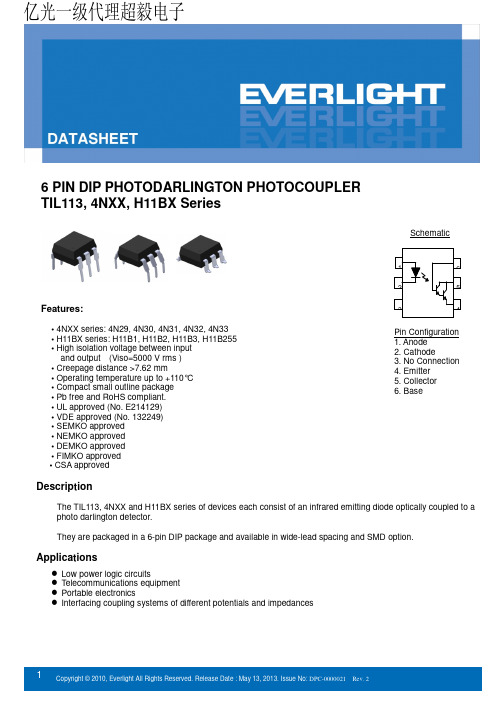
6 PIN DIP PHOTODARLINGTON PHOTOCOUPLERTIL113, 4NXX, H11BX SeriesFeatures:• 4NXX series: 4N29, 4N30, 4N31, 4N32, 4N33• H11BX series: H11B1, H11B2, H11B3, H11B255• High isolation voltage between inputand output (Viso=5000 V rms )• Creepage distance >7.62 mm• Operating temperature up to +110°C• Compact small outline package• Pb free and RoHS compliant.• UL approved (No. E214129)• VDE approved (No. 132249)• SEMKO approved• NEMKO approved• DEMKO approved• FIMKO approved• CSA approvedDescriptionThe TIL113, 4NXX and H11BX series of devices each consist of an infrared emitting diode optically coupled to a photo darlington detector.They are packaged in a 6-pin DIP package and available in wide-lead spacing and SMD option. ApplicationsLow power logic circuitsTelecommunications equipmentPortable electronicsInterfacing coupling systems of different potentials and impedancesSchematicPin Configuration1. Anode2. Cathode3. No Connection4. Emitter5. Collector6. BaseAbsolute Maximum Ratings (Ta=25℃)Parameter Symbol Rating UnitInput Forward current I F60 mA Peak forward current (1us, pulse) I FP 1 AReverse voltage V R 6 VPower dissipationNo derating required up to Ta = 100°C P D120 mW3.8 mW/°COutputPower dissipationDerating factor (above Ta = 80°C) P C 150 mW 6.5 mW/°CCollector-Emitter voltage V CEO55 VCollector-Base voltage V CBO55 VEmitter-Collector voltage V ECO7 VEmitter-Base voltage V EBO7 V Total power dissipation P TOT200 mW Isolation voltage V ISO5000 Vrms Operating temperature T OPR-55~+100 °C Storage temperature T STG-55~+125 °C Soldering temperature *2T SOL260 °C Notes:*1 AC for 1 minute, R.H.= 40 ~ 60% R.H. In this test, pins 1, 2 & 3 are shorted together, and pins 4, 5 & 6 are shorted together. *2 For 10 secondsElectro-Optical Characteristics (Ta=25℃unless specified otherwise)InputParameter Symbol Min. Typ.* Max. Unit ConditionForward Voltage V F- 1.2 1.5 V I F= 10mAI F= 50mA for H11B3Reverse Current I R- - 10 µA V R= 6VInput capacitance C in- 50 - pF V = 0, f = 1MHz OutputParameter Symbol Min. Typ.* Max. Unit ConditionCollector-Emitter darkcurrentI CEO- - 100 nA V CE= 10V Collector-Emitterbreakdown voltageBV CEO55 - - V I c=1mAEmitter-Collectorbreakdown voltageBV CBO55 - - V I C=0.1mA Emitter-Collectorbreakdown voltageBV ECO7 - - V I E=0.1mATransfer Characteristics (Ta=25°C unless specified otherwise)Parameter Symbol Min Typ. Max. Unit ConditionCurrent transfer ratio4N324N33CTR500 - -%I F= 10mA ,V CE= 10V 4N294N30100 - -4N31 50 - -H11B1 500 - -I F= 1mA ,V CE= 5VH11B2 200 - -H11B3 100 - -H11B255 100 - - I F= 10mA ,V CE= 5V TIL113 300 - - I F= 10mA ,V CE= 1VTransfer Characteristics (T a=25°C unless specified otherwise)Parameter Symbol Min Typ. Max. Unit ConditionCollector-e mitter saturation voltage4N294N304N324N33V CE(sat)- - 1.0VI F = 8mA ,I c = 2mA4N31TIL113- - 1.2 I F = 8mA ,I c = 2mAH11B1H11B2H11B3- - 1.0 I F = 1mA ,I c = 1mAH11B255 - - 1.0 I F = 50mA ,I c = 50mAIsolation resistance R IO1011- - ΩV IO = 500Vdc Input-outputCapacitanceC IO- 0.8 - pF V IO = 0, f = 1MHzTurn-on timeH11B1H11B2H11B3H11B255Ton- 25 -µsV CC = 10V, I F = 10mA,R L = 100Ω4N294N304N314N324N33TIL113- - 5V CC = 10V, I C = 50mA,I F=200mATurn-off timeH11B1H11B2H11B3H11B255Toff- 18 -µsV CC = 10V,I F = 10mA,R L = 100Ω4N324N33TIL113- - 100 VCC= 10V,I C = 50mA,I F=200mA 4N294N304N31- - 40* Typical values at T a = 25°CTypical Electro-Optical Characteristics CurvesV CCI FOutputFigure 7. Switching Time Test Circuit & WaveformsOrder InformationPart Number4NXXY(Z)-Vor H11BXY(Z)-Vor TIL113Y(Z)-VNoteXX = Part No. for 4NX series (29, 30, 31, 32 or 33)X = Part No. for H11BX series (1, 2, 3 or 255)Y = Lead form option (S, S1, M or none)Z = Tape and reel option (TA, TB or none).V = VDE safety (optional)Option Description Packing quantity None Standard DIP-6 65 units per tube M Wide lead bend (0.4 inch spacing) 65 units per tube S (TA) Surface mount lead form + TA tape & reel option 1000 units per reel S (TB) Surface mount lead form + TB tape & reel option 1000 units per reel S1 (TA) Surface mount lead form (low profile) + TA tape & reel option 1000 units per reel S1 (TB) Surface mount lead form (low profile) + TB tape & reel option 1000 units per reelPackage Dimension (Dimensions in mm) Standard DIP TypeOption M TypeOption S TypeOption S1 TypeRecommended pad layout for surface mount leadformDevice MarkingNotesEL denotes Everlight4N33TIL113H11B1 denotes Part NumberY denotes 1 digit Year codeWW denotes 2 digit Week codeV denotes VDE safety (optional)EL4N33YWWVELH11B1YWWVELTIL113YWWV11DPC-0000021 Rev. 2Tape & Reel Packing SpecificationsTape dimensionsDimension No. A B Do D1 E F Dimension(mm) 10.4±0.1 7.5±0.1 1.5±0.1 1.5+0.1/-01.75±0.1 7.5±0.1 Dimension No. Po P1 P2 t W K Dimension(mm) 4.0±0.1512±0.12.0±0.10.35±0.0316.0±0.24.5±0.112Copyright © 2010, Everlight All Rights Reserved. Release Date : October 5, 2012. Issue No: DPC-0000021 Rev. 2Precautions for Use1. Soldering Condition1.1 (A) Maximum Body Case Temperature Profile for evaluation of Reflow ProfileNote: Reference: IPC/JEDEC J-STD-020DPreheatTemperature min (T smin ) 150 °C Temperature max (T smax )200°CTime (T smin to T smax ) (t s )60-120 seconds Average ramp-up rate (T smax to T p )3 °C/second maxOtherLiquidus Temperature (T L )217 °C Time above Liquidus Temperature (t L ) 60-100 sec Peak Temperature (T P )260°C Time within 5 °C of Actual Peak Temperature: T P - 5°C 30 sRamp- Down Rate from Peak Temperature 6°C /second max. Time 25°C to peak temperature 8 minutes max. Reflow times 3 times.DISCLAIMER1. Above specification may be changed without notice. EVERLIGHT will reserve authority on material change for abovespecification.2. When using this product, please observe the absolute maximum ratings and the instructions for using outlined in thesespecification sheets. EVERLIGHT assumes no responsibility for any damage resulting from use of the product which does not comply with the absolute maximum ratings and the instructions included in these specification sheets.3. These specification sheets include materials protected under copyright of EVERLIGHT corporation. Please don’treproduce or cause anyone to reproduce them without EVERLIGHT’s consent.13Rev. 2。
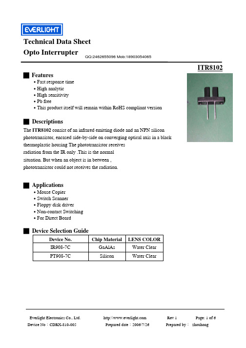
ITR8102亿光U型槽型光耦,红外线对射式对管,对射式光电开关
Parameter Power Dissipation at(or below) 25℃ Free Air Temperature Input Reverse Voltage Forward Current Peak Forward Current (*1) Pulse width ≦100μs, Duty cycle=1% Collector Power Dissipation Output Collector Current Collector-Emitter Voltage Emitter-Collector Voltage Operating Temperature Storage Temperature Lead Soldering Temperature (*2) (1/16 inch form body for 5 seconds) (*1) tw=100 μsec. , T=10 msec. Parameter Forward Voltage Reverse Current Peak Wavelength View Angle Dark Current Output C-E Saturation Voltage Collect Current Transfer Rise time Characteristics Fall time Symbol VF IR λP 2θ1/2 ICEO VCE(sat) IC(ON) tr tf Symbol Pd VR IF IFP PC IC B VCEO B VECO Topr Tstg Tsol (*2) t=5 Sec Max. 1.5 10 ----100 0.4
1
Solder Heat
亿光槽型对射式光电开关 ITR9707
亿光槽型对射式光电开关ITR9707鼠标专用光遮断器
文章出处:广州市超毅电子有限公司
光电开关(ITR)英文为PhotoInterrupter中文为光遮断器,光断续器,光电开关。
亿光光电开关也属于红外线不可见光产品,是一种小型光电元器件,它可以检测出其接收到的光强的变化。
光电开关是光学电子装置的一种,它是通过电信号与光信号互为转换,其组合了发光与受光元件,用以检查物体为目的之一种装置。
亿光代理商超毅电子在此推荐一款亿光光电开关ITR9707,是超毅电子主推产品。
在代理亿光产品中也是销售也是名列前茅的,那它有什么优势才让市场那么受欢迎呢?下面我们一起去了解下。
.
亿光光电开关ITR9707结构:是款槽型对射式光电开关,由一个红外发光二极管和一个NPN型硅光电晶体管组成的光电开关,光电晶体管接收红外辐射了。
这是正常的情况。
但当对象之间有物体时,光电晶体管无法接收辐射红外线了。
亿光光电开关ITR9707参数图:
亿光光电开关ITR9707的优势:光的发射与接收距离宽(5.2mm),能快速的响应时间,截止可见波长λP=940海里,传感度精确,PWB封装,无铅,产品符合RoHS标准。
主要应用在鼠标,复印机,开关扫描仪,软盘驱动程序,无触点开关和pc看板等上面。
亿光光电开关ITR9707尺寸图:
亿光代理商超毅电子是亿光的15年合作伙伴,拥有着丰富的亿光光电开关的市场经验,因此,如果对于槽型对射式光电开关和反射式光电开关的相关应用资料跟规格参数,可直接联系超毅,超毅电子会为您提供最专业的技术支持。
免费咨询热线:4008-800-932。
R8103规格书(中文版)

ӨJA
110
℃/W
ESD 保护(人体模式) 储存温度 结温 焊接温度(锡焊,10 秒)
ESD~150
℃
150
℃
300
℃
注:超出所列的极限参数可能导致器件的永久性损坏。以上给出的仅仅是极限范围,在这样的极限条件下工作,器件的技术指标将得不到保证,
长期在这样的工作条件下还会影响可靠性
R8103 内部集成了丰富的保护功能,包括过压保护,短路保护,逐周期电流保护,温度保护和软启动 等。
R8103 具有极低的启动电流和工作电流,可在全电压交流输入(85VAC~265VAC)或 8 到 450V 直流输入 电压内高效驱动 LED。
应用范围
LED 驱动电源。
管脚排列
数据手册 3.0 23553Q68872黄R1376032电5070
FB
前沿消隐
输 出 驱 动
COMP
图 1 R8103 功能框图
DRAIN SOURCE
CS
数据手册 3.0
-3-
2012-09
R8103 应用信息
R8103 是非隔离降压型恒流驱动器,内部集成高压 600V MOSFET,采用 DIP-8 封装,LED 电流可以输 出高达 350mA;R8103 采用谷底开关模式,自适应电感感量和输出电压的变化,只需要很少的外围器件 来实现恒流驱动 LED。
输出开(短)路保护
R8103 内部集成了输出开(短)路保护 , R8103 一旦检测到输出开(短)路,系统会自动进入打嗝模式, 直到开(短)路保护条件除去。
过热保护
R8103 内部集成了过热保护功能,触发过热保护温度为典型 140℃,当 R8103 被触发过热保护后, 芯片只有降到 120℃之后,才能重新正常工作。
详解光耦EL817的重要参数

详解光耦EL817的重要参数详解光耦EL817的重要参数——CTR值 CTR:发光管的电流和光敏三极管的电流比的最小值。
隔离电压:发光管和光敏三极管的隔离电压的最小值。
光耦的技术参数主要有发光二极管正向压降VF、正向电流IF、电流传输比CTR、输入级与输出级之间的绝缘电阻、集电极-发射极反向击穿电压V(BR)CEO、集电极-发射极饱和压降VCE(sat)。
此外,在传输数字信号时还需考虑上升时间、下降时间、延迟时间和存储时间等参数。
集电极-发射极电压:集电极-发射极之间的耐压值的最小值光耦什么时候导通?什么时候截至?普通光耦合器的CTR-IF特性曲线呈非线性,在IF较小时的非线性失真尤为严重,因此它不适合传输模拟信号。
线性光耦合器的CTR-IF特性曲线具有良好的线性度,特别是在传输小信号时,其交流电流传输比(ΔCTR=ΔIC/ΔIF)很接近于直流电流传输比CTR值。
因此,它适合传输模拟电压或电流信号,能使输出与输入之间呈线性关系。
这是其重要特性。
电流传输比是光耦合器的重要参数,通常用直流电流传输比来表示。
当输出电压保持恒定时,它等于直流输出电流IC与直流输入电流IF的百分比。
采用一只光敏三极管的光耦合器,CTR的范围大多为20%,300%(如4N35),而pc817则为80%,160%,台湾亿光(如EL817)可达50%,600%。
这表明欲获得同样的输出电流,后者只需较小的输入电流。
因此,CTR参数与晶体管的hFE有某种相似之处。
使用光电耦合器主要是为了提供输入电路和输出电路间的隔离,在设计电路时,必须遵循下列所选用的光电耦合器件必须符合国内和国际的有关隔离击穿电压的标准;由台湾亿光生成生产的EL817系列(如EL817B-F、EL817C-F)光耦合器,目前在国内应用地十分普遍。
鉴于此类光耦合器呈现开关特性,其线性度差,适宜传输数字信号(高、低电平),可以用于单片机的输出隔离;所选用的光耦器件必须具有较高的耦合系数。
亿光光电开关ITR9909
+Opto Interrupter ITR9909Features․Fast response time ․High analytic․Cut-off visible wavelength λp=940nm ․High sensitivity ․Pb free․This product itself will remain within RoHS compliant versionDescription․The ITR9909 consist of an infrared emitting diode and an NPN silicon phototransistor,encased side-by-side on converging optical axis in a black thermoplastic housing,․The phototransistor receives radiation from the IR only .This is the normal situation. ․But when an object is in between , phototransistor could not receives the radiation.․For additional component information , please refer to IR and PTApplications․Mouse Copier ․Switch Scanner ․Floppy disk driver․Non-contact Switching ․For Direct Board亿光一级代理商超毅电子Device Selection GuideDevice No.ChipMaterialsLens ColorIR GaAlAs BluePT Silicon BlackAbsolute Maximum Ratings(Ta=25)Parameter Symbol Ratings Unit Power Dissipation at(or below) 25 Free AirTemperaturePd75mW Reverse Voltage V R5VForward Current I F50mA InputPeak Forward Current (*1)Pulse width100μs,Duty cycle=1%I FP1ACollector Power Dissipation Pd75mWCollector Current I C50mACollector-Emitter Voltage B V CEO30V OutputEmitter-Collector Voltage B V ECO5V Operating Temperature Topr-25~+85 Storage Temperature Tstg-40~+85 Lead Soldering Temperature (*2)(1/16 inch form body for 5 seconds)Tsol260 (*1) tw=100 μsec. , T=10 msec. (*2) t=5 SecElectro-Optical Characteristics (Ta=25)ParameterSymbolMin.Typ.Max.UnitConditions --- 1.21.5I F =20mA--- 1.4 1.85IF=100mA,tp=100 s,tp/T=0.01Forward VoltageVF--- 2.64.0VIF=1A,tp=100 s,tp/T=0.01Reverse Current I R ------10μA V R =5V InputPeak Wavelength λP ---940---nm I F =20mADark C urrentI CEO ------100nA V CE =20V,Ee=0mW/cm2OutputC-E Saturation VoltageV CE (sat)------0.4VI C =2mAEe=1mW/cm 2Collect CurrentI C (ON)200------uA V CE =5V IF=20mA Rise timet r ---15---μsec TransferCharacteristics Fall timet f ---15---μsecV CE =5V,I C =1mA ,R L =1000Ω-201.0-10020107007257507758008258508759009259509751000102510500.00.2R e l a Wavelength (nm)-20402006010080Relative Radiant Intensity vs Forward Current Relative Radiant Intensity vs Angular Displacement110080007000.290010001300110100CRelative Collector Current vs. Ambient Temperature Collector Current vs. Irradiance502585751002Typical Electrical/Optical/Characteristics Curves for ITR Relative Collector Current vs DIistance Between SensorPackage DimensionNote: Tolerances unless dimensions ±0.25mmPacking Quantity Specification1.150PCS/1Bag, 5Bags/1Box2.10Boxes/1CartonNotes1.Above specification may be changed without notice. EVERLIGHT will reserve authority onmaterial change for above specification.2.When using this product, please observe the absolute maximum ratings and the instructionfor using outlined in these specification sheets. EVERLIGHT assumes no responsibility forany damage resulting from use of the product which does not comply with the absolutemaximum ratings and the instructions included in these specification sheets.3.These specification sheets include materials protected under copyright of EVERLIGHT corporation.Please don’t reproduce or cause anyone to reproduce them without EVERLIGHT’s consent.。
el3083光耦参数

el3083光耦参数el3083光耦是一种常用的光电器件,广泛应用于各种电子设备中。
它由发光二极管(LED)和光敏三极管(光电二极管)组成,通过光的转换来实现电信号的隔离和传输。
光耦的参数对于其性能和应用范围具有重要影响,下面将对el3083光耦的主要参数进行详细介绍。
1. 光耦输入电流(IF):光耦输入电流是指光耦所需的驱动电流,通常以毫安(mA)为单位。
IF值的选择应根据具体应用需求和光耦的额定工作电流范围来确定,过小的IF值可能无法正常驱动光耦,而过大的IF值则可能导致光耦工作不稳定或损坏。
2. 光耦输出电流(IC):光耦输出电流是指光耦输出端的电流,通常以毫安(mA)为单位。
IC值的大小取决于光耦的响应速度和驱动电流IF的大小,一般情况下,IC值越大,表示光耦的输出能力越强。
3. 光耦输入电压(VF):光耦输入电压是指光耦的工作电压范围,通常以伏特(V)为单位。
VF值的选择应根据光耦的额定工作电压范围来确定,过小或过大的VF值可能导致光耦无法正常工作或损坏。
4. 光耦输出电压(VCE):光耦输出电压是指光耦输出端的电压,通常以伏特(V)为单位。
VCE值的大小取决于光耦的输出电流IC和光耦的负载电阻值,一般情况下,VCE值越小,表示光耦的输出能力越强。
5. 光耦绝缘电压(VR):光耦绝缘电压是指光耦输入端和输出端之间的绝缘电压,通常以伏特(V)为单位。
VR值的大小决定了光耦的隔离性能,一般情况下,VR值越大,表示光耦的隔离能力越强。
6. 光耦响应时间(tR、tF):光耦响应时间是指光耦从接收到输入光信号到输出电流上升或下降到一定百分比所需的时间。
tR表示上升时间,tF表示下降时间。
光耦的响应时间越短,表示其响应速度越快。
7. 光耦工作温度范围(Tamb):光耦工作温度范围是指光耦正常工作的环境温度范围。
Tamb值的选择应根据光耦的额定工作温度范围来确定,过高或过低的环境温度可能导致光耦无法正常工作或损坏。