
亿光光耦EL3023
6PIN DIP RANDOM-PHASE TRIAC DRIVER PHOTOCOUPLER EL301X, EL302X, EL305X SeriesFeatures:• Peak breakdown voltage -250V: EL301X -400V: EL302X -600V: EL305X• High isolation voltage between input and output (Viso=5000 V rms )• Compact dual-in-line package • Pb free and RoHS compliant.•UL and cUL approved(No. E214129)• VDE approved (No.132249)• SEMKO approved • NEMKO approved • DEMKO approved •FIMKO approvedDescriptionThe EL301X, EL302X and EL305X series of devices each consist of a GaAs infrared emitting diode optically coupled to a monolithic silicon random phase photo Triac.They are designed for interfacing between electronic controls and power triacs to control resistive and inductive loads for 115 to 240 VAC operations.Applications●Solenoid/valve controls ●Lamp ballasts●Static AC power switch●Interfacing microprocessors to 115 to 240Vac peripherals ●Incandescent lamp dimmers ●Temperature controls ●Motor controlsSchematic126543Pin Configuration 1. Anode 2. Cathode3. No Connection4. Terminal5. Substrate(do not connect)6. Terminal亿光一级代理商超毅电子Absolute Maximum Ratings (Ta=25 )Parameter Symbol Rating Unit Input Forward current I F60mA Reverse voltage V R6VPower dissipationDerating factor (above T a = 85 C)P D100mW3.8mW/°COutputOff-state OutputTerminal Voltage EL301XV DRM250V EL302X400EL305X600Peak Repetitive Surge Current(pw=100μs,120pps)I TSM1A On-State RMS Current I T(RMS)100mAPower dissipationDerating factor (above T a = 85 C)P C300mW7.4mW/Total power dissipation P TOT330mW Isolation voltage*1V ISO5000Vrms Operating temperature T OPR-55 to 100 Storage temperature T STG-55 to 125 Soldering Temperature*2T SOL260 Notes:*1AC for 1 minute, R.H.= 40 ~ 60% R.H. In this test, pins 1, 2&3are shorted together, and pins4, 5 & 6are shorted together. *2 For 10 secondsElectro-Optical Characteristics (Ta=25 unless specified otherwise)InputParameter Symbol Min.Typ.*Max.Unit Condition Forward Voltage V F- 1.18 1.5V I F=10mA Reverse Leakage current I R--10µA V R=6V OutputParameter Symbol Min.Typ.*Max.Unit ConditionPeak Blocking Current I DRM--100nA V DRM = Rated V DRM I F=0mAPeak On-state Voltage V TM-- 2.5V I TM=100mA peak, I F=Rated I FTCritical Rate of Rise off-state Voltage EL301XEL302X dv/dt-100-V/µsV PEAK=Rated V DRM,I F=0 (Fig. 8)EL305X1000--V PEAK=400V,I F=0 (Fig. 8)Transfer CharacteristicsParameter Symbol Min.Typ.*Max.Unit ConditionLED Trigger Current EL3020I FT30mA Main terminal Voltage=3V EL3010EL3021EL3051--15EL3011EL3022EL3052--10EL3012EL3023EL3053--5Holding Current I H-250-µA * Typical values at T a= 25°CTypical Electro-Optical Characteristics CurvesFigure 8. Static dv/dt Test Circuit & WaveformMeasurement MethodThe high voltage pulse is set to the required V PEAK value and applied to the D.U.T. output side through the RC circuit above. LED current is not applied. The waveform V T is monitored using a x100 scope probe. By varying R TEST , the dv/dt (slope) is increased, until the D.U.T. is observed to trigger (waveform collapses). The dv/dt is then decreased until the D.U.T. stops triggering. At this point, τRC is recorded and the dv/dt calculated.For example, V PEAK = 400V for EL302X series. The dv/dt value is calculated as follows:V PEAKApplied V T WaveformτRC0.632 x V PEAK50 Ω10 k ΩD.U.T.R TESTHigh Voltage Pulse SourceC TESTV T A KT1T20.63 x 400τRCdv/dt = = 252τRC0.632 x V PEAK τRCdv/dt =Order InformationPart NumberEL301XY(Z)-Vor EL302XY(Z)-Vor EL305XY(Z)-VNoteX = Part No. for EL301x (0, 1 or 2)X = Part No. for EL302x, EL305x (1, 2 or 3)Y = Lead form option (S, S1, M or none)Z = Tape and reel option (TA, TB or none).V = VDE safety approved (optional)Option Description Packing quantity None Standard DIP-665 units per tube M Wide lead bend (0.4 inch spacing)65 units per tube S Surface mount lead form65 units per tube S(TA)Surface mount lead form + TA tape & reel option1000 units per reel S (TB)Surface mount lead form + TB tape & reel option1000 units per reel S1 (TA)Surface mount lead form (low profile) + TA tape & reel option1000 units per reel S1 (TB)Surface mount lead form (low profile) + TB tape & reel option1000 units per reelPackage Dimension(Dimensions in mm) Standard DIP TypeOption M TypeOption S TypeOption S1 TypeRecommended pad layout for surface mount leadformDevice MarkingNotesEL denotes EVERLIGHT3053 denotes Device NumberY denotes 1 digit Year codeWW denotes 2 digit Week codeVdenotes VDE (optional)EL3053YWWVTape dimensionsDimension No.A B Do D1E F Dimension (mm)10.4±0.17.5±0.1 1.5±0.1 1.5+0.1/-01.75±0.17.5±0.1Dimension No.Po P1P2t W K Dimension (mm)4.0±0.1512±0.12.0±0.10.35±0.0316.0±0.24.5±0.1Revision : 7Release Date:2014-09-24 17:43:02.011Copyright © 2010, Everlight All Rights Reserved.Release Date:September 3, 2014. Issue No:DPC-0000059 Rev.7Precautions for Use1. Soldering Condition1.1 (A) Maximum Body Case Temperature Profile for evaluation of Reflow ProfileNote: Reference: IPC/JEDEC J-STD-020DPreheatTemperature min (T smin ) 150 °C Temperature max (T smax )200°CTime (T smin to T smax ) (t s )60-120 seconds Average ramp-up rate (T smax to T p ) 3 °C/second maxOtherLiquidus Temperature (T L )217 °C Time above Liquidus Temperature (t L )60-100 sec Peak Temperature (T P )260°C Time within 5 °C of Actual Peak Temperature: T P -5°C 30 sRamp-Down Rate from Peak Temperature 6°C /second max.Time 25°C to peak temperature 8 minutes max.Reflow times 3 times .Revision : 7Release Date:2014-09-24 17:43:02.012 2010, Everlight All Rights Reserved.Release Date:September 3, 2014. Issue No:DPC-0000059 Rev.70 DISCLAIMER1.Above specification may be changed without notice. EVERLIGHT will reserve authority on material change for abovespecification.2.When using this product, please observe the absolute maximum ratings and the instructions for using outlined in thesespecification sheets. EVERLIGHT assumes no responsibility for any damage resulting from use of the product which does not comply with the absolute maximum ratings and the instructions included in these specification sheets.3.These specification sheets include materials protected under copyright of EVERLIGHT corporation. Please don’treproduce or cause anyone to reproduce them without EVERLIGHT’s consent.。
亿光EL30系列光耦及过零检测
亿光亿光过零检测过零检测过零检测光耦光耦
驱动大功率交流器件时常用双向可控硅进行功率控制,根据控制方式的不同有过零控制和移相控制。
不管哪种控制都要对零点进行检测,因为双向过控硅的特性是到了交流的零点,可控硅会自动关闭输出。
我们检测零点目的就是可控硅在零点关闭输出后,我们可以根据功率的需求选择时间来重新触发可控硅。
但对于单片机弱电直接控制交流肯定是不现实的,用继电器控制只能实现简单的慢速的开关量控制,而如果要实现功率调节,我们就需要用光特性的固态继电器,这种器件比较贵。
而假如用光耦肯定也是不行的,因为普通的光耦是单向器件,对于交流的网电它是不能实现控制的。
在这种情况下,我们最好的选择就是用EL30XX 系列的光控
可控硅,用得最多的EL3053和EL3083,它们的前端触发电流都是5mA ,隔离电压达到5000Vrms ,适合于对电绝缘特性要求高的工控或医疗电子行业。
EL3053和EL3083的主要区别就是EL3083有过零检测,MOC3053没有过零检测,对于有过零检测功能的EL3083,它每次在过零点的时候会判断有没有光输入,即有没有前置电流If ,如果有If ,那么在这个周期之内,它是导通的,所以它只能决定一个网电源周期内它是不是导通的,而不能决定在一个周期的某一个时刻
开始导通。
基于这种特性我们可以用它来实现过零控制,过零控制的缺点是控制精度低,优点是对电网没有污染。
对于没有过零检测的EL3053来说,它在有光输入的时刻开始到这个周期的结束它都是导通的。
基于这种特性,如果我们已经检测到了零点,我们就可以在零点的时刻开始延时一段时间来输入前置电流If,用它来实现移相检测。
QQ:312066116。
亿光光耦ELM452

Revision :3 © 1 Copyright LifecyclePhase:
Date:2013-07-15 2010, Everlight All Rights Reserved. Release Date : May 13, 2013. Issue Release No: DPC-0000113 Rev.3 Expired Period: Forever
Revision :3 5 Copyright © LifecyclePhase:
2010, Everlight All Rights Reserved. Release Date : May 13, 2013. Issue No:DPC-0000113 Rev.3
Release Date:2013-07-15 14:59:03.0 Expired Period: Forever
Pin Configuration 1. Anode 3. Cathode 4. Gnd 5. Vout 6. VCC
Description
The ELM452 and ELM453 devices each consist of an infrared emitting diode, optically coupled to a high speed photo detector transistor. A separate connection for the photodiode bias and output-transistor collector increase the speed by several orders of magnitude over conventional phototransistor couplers by reducing the base-collector capacitance of the input transistor.The devices are packaged in industry standard 5pin SOP packages and are suitable for surface mounting.
MOC3023_光耦.pdf

Fig. 4 LED Current Required to Trigger vs. LED Pulse Width
25
1.3
TRIGGER CURRENT - I FT (NORMALIZED)
TRIGGER CURRENT - I FT (NORMALIZED)
20
NORMALIZED TO: PWin ≥ 100 µs
2 OF 8
10/31/01 DS300255
6-PIN DIP RANDOM-PHASE OPTOISOLATORS TRIAC DRIVER OUTPUT
(250/400 VOLT PEAK)
MOC3010M
1.8
MOC3011M
MOC3012M
MOC3020M
100
6
4
10
2
1
0 25 30 40 50 60 70 80 90
Ambient Temperature - TA (oC)
0.1 -40 -20 0 20 40 60
o
80
100
TA, AMBIENT TEMPERATURE ( C)
DS300255
10/31/01
3 OF 8
Note 1. Isolation surge voltage, VISO, is an internal device dielectric breakdown rating. For this test, Pins 1 and 2 are common, and Pins 4, 5 and 6 are common.
Peak Blocking Current,Either Direction Rated VDRM, IF = 0 (note 1) Peak On-State Voltage,Either Direction ITM = 100 mA peak, IF = 0 Critical Rate of Rise of Off-State Voltage IF = 0 (figure 5, note2)
亿光光耦TIL113
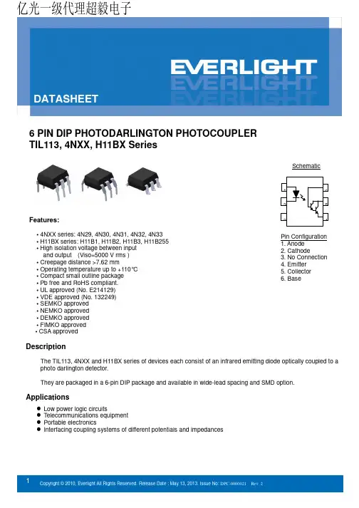
6 PIN DIP PHOTODARLINGTON PHOTOCOUPLERTIL113, 4NXX, H11BX SeriesFeatures:• 4NXX series: 4N29, 4N30, 4N31, 4N32, 4N33• H11BX series: H11B1, H11B2, H11B3, H11B255• High isolation voltage between inputand output (Viso=5000 V rms )• Creepage distance >7.62 mm• Operating temperature up to +110°C• Compact small outline package• Pb free and RoHS compliant.• UL approved (No. E214129)• VDE approved (No. 132249)• SEMKO approved• NEMKO approved• DEMKO approved• FIMKO approved• CSA approvedDescriptionThe TIL113, 4NXX and H11BX series of devices each consist of an infrared emitting diode optically coupled to a photo darlington detector.They are packaged in a 6-pin DIP package and available in wide-lead spacing and SMD option. ApplicationsLow power logic circuitsTelecommunications equipmentPortable electronicsInterfacing coupling systems of different potentials and impedancesSchematicPin Configuration1. Anode2. Cathode3. No Connection4. Emitter5. Collector6. BaseAbsolute Maximum Ratings (Ta=25℃)Parameter Symbol Rating UnitInput Forward current I F60 mA Peak forward current (1us, pulse) I FP 1 AReverse voltage V R 6 VPower dissipationNo derating required up to Ta = 100°C P D120 mW3.8 mW/°COutputPower dissipationDerating factor (above Ta = 80°C) P C 150 mW 6.5 mW/°CCollector-Emitter voltage V CEO55 VCollector-Base voltage V CBO55 VEmitter-Collector voltage V ECO7 VEmitter-Base voltage V EBO7 V Total power dissipation P TOT200 mW Isolation voltage V ISO5000 Vrms Operating temperature T OPR-55~+100 °C Storage temperature T STG-55~+125 °C Soldering temperature *2T SOL260 °C Notes:*1 AC for 1 minute, R.H.= 40 ~ 60% R.H. In this test, pins 1, 2 & 3 are shorted together, and pins 4, 5 & 6 are shorted together. *2 For 10 secondsElectro-Optical Characteristics (Ta=25℃unless specified otherwise)InputParameter Symbol Min. Typ.* Max. Unit ConditionForward Voltage V F- 1.2 1.5 V I F= 10mAI F= 50mA for H11B3Reverse Current I R- - 10 µA V R= 6VInput capacitance C in- 50 - pF V = 0, f = 1MHz OutputParameter Symbol Min. Typ.* Max. Unit ConditionCollector-Emitter darkcurrentI CEO- - 100 nA V CE= 10V Collector-Emitterbreakdown voltageBV CEO55 - - V I c=1mAEmitter-Collectorbreakdown voltageBV CBO55 - - V I C=0.1mA Emitter-Collectorbreakdown voltageBV ECO7 - - V I E=0.1mATransfer Characteristics (Ta=25°C unless specified otherwise)Parameter Symbol Min Typ. Max. Unit ConditionCurrent transfer ratio4N324N33CTR500 - -%I F= 10mA ,V CE= 10V 4N294N30100 - -4N31 50 - -H11B1 500 - -I F= 1mA ,V CE= 5VH11B2 200 - -H11B3 100 - -H11B255 100 - - I F= 10mA ,V CE= 5V TIL113 300 - - I F= 10mA ,V CE= 1VTransfer Characteristics (T a=25°C unless specified otherwise)Parameter Symbol Min Typ. Max. Unit ConditionCollector-e mitter saturation voltage4N294N304N324N33V CE(sat)- - 1.0VI F = 8mA ,I c = 2mA4N31TIL113- - 1.2 I F = 8mA ,I c = 2mAH11B1H11B2H11B3- - 1.0 I F = 1mA ,I c = 1mAH11B255 - - 1.0 I F = 50mA ,I c = 50mAIsolation resistance R IO1011- - ΩV IO = 500Vdc Input-outputCapacitanceC IO- 0.8 - pF V IO = 0, f = 1MHzTurn-on timeH11B1H11B2H11B3H11B255Ton- 25 -µsV CC = 10V, I F = 10mA,R L = 100Ω4N294N304N314N324N33TIL113- - 5V CC = 10V, I C = 50mA,I F=200mATurn-off timeH11B1H11B2H11B3H11B255Toff- 18 -µsV CC = 10V,I F = 10mA,R L = 100Ω4N324N33TIL113- - 100 VCC= 10V,I C = 50mA,I F=200mA 4N294N304N31- - 40* Typical values at T a = 25°CTypical Electro-Optical Characteristics CurvesV CCI FOutputFigure 7. Switching Time Test Circuit & WaveformsOrder InformationPart Number4NXXY(Z)-Vor H11BXY(Z)-Vor TIL113Y(Z)-VNoteXX = Part No. for 4NX series (29, 30, 31, 32 or 33)X = Part No. for H11BX series (1, 2, 3 or 255)Y = Lead form option (S, S1, M or none)Z = Tape and reel option (TA, TB or none).V = VDE safety (optional)Option Description Packing quantity None Standard DIP-6 65 units per tube M Wide lead bend (0.4 inch spacing) 65 units per tube S (TA) Surface mount lead form + TA tape & reel option 1000 units per reel S (TB) Surface mount lead form + TB tape & reel option 1000 units per reel S1 (TA) Surface mount lead form (low profile) + TA tape & reel option 1000 units per reel S1 (TB) Surface mount lead form (low profile) + TB tape & reel option 1000 units per reelPackage Dimension (Dimensions in mm) Standard DIP TypeOption M TypeOption S TypeOption S1 TypeRecommended pad layout for surface mount leadformDevice MarkingNotesEL denotes Everlight4N33TIL113H11B1 denotes Part NumberY denotes 1 digit Year codeWW denotes 2 digit Week codeV denotes VDE safety (optional)EL4N33YWWVELH11B1YWWVELTIL113YWWV11DPC-0000021 Rev. 2Tape & Reel Packing SpecificationsTape dimensionsDimension No. A B Do D1 E F Dimension(mm) 10.4±0.1 7.5±0.1 1.5±0.1 1.5+0.1/-01.75±0.1 7.5±0.1 Dimension No. Po P1 P2 t W K Dimension(mm) 4.0±0.1512±0.12.0±0.10.35±0.0316.0±0.24.5±0.112Copyright © 2010, Everlight All Rights Reserved. Release Date : October 5, 2012. Issue No: DPC-0000021 Rev. 2Precautions for Use1. Soldering Condition1.1 (A) Maximum Body Case Temperature Profile for evaluation of Reflow ProfileNote: Reference: IPC/JEDEC J-STD-020DPreheatTemperature min (T smin ) 150 °C Temperature max (T smax )200°CTime (T smin to T smax ) (t s )60-120 seconds Average ramp-up rate (T smax to T p )3 °C/second maxOtherLiquidus Temperature (T L )217 °C Time above Liquidus Temperature (t L ) 60-100 sec Peak Temperature (T P )260°C Time within 5 °C of Actual Peak Temperature: T P - 5°C 30 sRamp- Down Rate from Peak Temperature 6°C /second max. Time 25°C to peak temperature 8 minutes max. Reflow times 3 times.DISCLAIMER1. Above specification may be changed without notice. EVERLIGHT will reserve authority on material change for abovespecification.2. When using this product, please observe the absolute maximum ratings and the instructions for using outlined in thesespecification sheets. EVERLIGHT assumes no responsibility for any damage resulting from use of the product which does not comply with the absolute maximum ratings and the instructions included in these specification sheets.3. These specification sheets include materials protected under copyright of EVERLIGHT corporation. Please don’treproduce or cause anyone to reproduce them without EVERLIGHT’s consent.13Rev. 2。
MOC3023中文资料

IMPORTANT NOTICETexas Instruments (TI) reserves the right to make changes to its products or to discontinue any semiconductor product or service without notice, and advises its customers to obtain the latest version of relevant information to verify, before placing orders, that the information being relied on is current.TI warrants performance of its semiconductor products and related software to the specifications applicable at the time of sale in accordance with TI’s standard warranty. Testing and other quality control techniques are utilized to the extent TI deems necessary to support this warranty. Specific testing of all parameters of each device is not necessarily performed, except those mandated by government requirements.Certain applications using semiconductor products may involve potential risks of death, personal injury, or severe property or environmental damage (“Critical Applications”).TI SEMICONDUCTOR PRODUCTS ARE NOT DESIGNED, INTENDED, AUTHORIZED, OR WARRANTED TO BE SUITABLE FOR USE IN LIFE-SUPPORT APPLICATIONS, DEVICES OR SYSTEMS OR OTHER CRITICAL APPLICATIONS.Inclusion of TI products in such applications is understood to be fully at the risk of the customer. Use of TI products in such applications requires the written approval of an appropriate TI officer. Questions concerning potential risk applications should be directed to TI through a local SC sales office.In order to minimize risks associated with the customer’s applications, adequate design and operating safeguards should be provided by the customer to minimize inherent or procedural hazards.TI assumes no liability for applications assistance, customer product design, software performance, or infringement of patents or services described herein. Nor does TI warrant or represent that any license, either express or implied, is granted under any patent right, copyright, mask work right, or other intellectual property right of TI covering or relating to any combination, machine, or process in which such semiconductor products or services might be or are used.Copyright © 1995, Texas Instruments Incorporated。
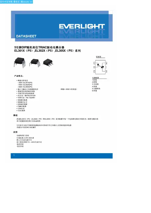
EL3021(P5)-V中文资料(EVERLIGHT)中文数据手册「EasyDatasheet - 矽搜」
IFT
-
mA
主候机楼
Voltage=3V
防护持电流
IH
a
-
µA
*在T典型值
= 25°C
3
芯片中文手册,看全文,戳
数据表 5引脚 DIP随机相位TRIAC驱动光电耦合器 EL301X(P5),EL302X(P5),EL305X(P5)系列
典型光电特性曲线
4
芯片中文手册,看全文,戳
EL301X EL302X EL305X
峰值重复浪涌电流 功耗 降额系数(以上T
a=
V
A mW mW/
85 C)
℃
总功耗 隔离电压 工作温度 储存温度 焊接温度* 笔记:
2 *1
mW Vrms
V ISO T OPR T STG T SOL
℃ ℃ ℃
*1 交流进行1分钟,RH = 40〜60%RH在本试验中,引脚1,2和3被短接在一起,和引脚4,6被短接在一起. * 2防护持10秒
℃
参数
符号
等级
单元
Input
正向电流 反向电压 功耗 无需达至T降级
a=
IF VR PD
60 6 100
mA V mW
毫瓦/度C
85° C
3.8 250 V DRM 400 600 ITSM PC 7.4 P TOT 330 5000 -55至100 -55至125 260 1 300
产量 断态输出 端电压
引脚配置 1.阳极 2.阴极 3.无连接 4.终端 5.引脚剪切 6.终端
所述EL301X(P5),EL302X(P5)和EL305X(P5)系列装置中每一个包括砷化镓红外线发光二极管光耦合到 单片硅随机相位照片双向晶闸管. 它们是专为电子控制和电源端双向可控硅开关之间接口,以控制电阻和电感 负载为115至240 VAC操作
moc3023引脚参数
MOC3023引脚参数导言M O C3023是一种隔离型三端输出光耦合器,它在电子设备中广泛应用。
本文将介绍M OC3023的引脚参数及其作用,帮助读者更好地理解和应用这款器件。
引脚说明M O C3023的引脚共有6个,分别为:1.`1`脚:主光电耦合器的阳极(A1)。
2.`2`脚:主光电耦合器的阴极(A2)。
3.`3`脚:辅助开关阴极(G2)。
4.`4`脚:辅助开关阳极(A2)。
5.`5`脚:未连接引脚(N C)。
6.`6`脚:未连接引脚(N C)。
引脚功能分析1.主光电耦合器引脚主光电耦合器引脚(`1`脚和`2`脚)用于输入控制信号,实现光耦合器的隔离功能。
其中,`1`脚为阳极,`2`脚为阴极。
主光电耦合器引脚的主要特点有:-高隔离电压:主光电耦合器引脚间的隔离电压可达数千伏,保证了输入信号的安全与可靠。
-低驱动电流:主光电耦合器引脚的驱动电流较低,能够节省能量,并减少热量的产生。
2.辅助开关引脚辅助开关引脚(`3`脚和`4`脚)可用于控制外部开关电路。
其中,`3`脚为辅助开关阴极,`4`脚为辅助开关阳极。
辅助开关引脚的主要特点有:-高耐压能力:辅助开关引脚能够承受较高的电压,在外部开关电路中起到可靠的控制作用。
-小型化设计:辅助开关引脚采用小型化设计,适用于紧凑的电路布局环境。
3.未连接引脚M O C3023的剩余两个引脚(`5`脚和`6`脚)为未连接引脚,在使用中不需要接触到其他电路。
未连接引脚的设计原因是为了保证产品的兼容性和应用灵活性,使得M O C3023能够适应多种不同的电路布局和连接方式。
总结M O C3023是一款常用的光耦合器,它具有较高的隔离电压、低驱动电流和高耐压能力等特点。
通过本文所介绍的引脚参数,我们可以更好地理解和应用这款器件。
(完)。
3063光耦参数
3063光耦参数光耦是一种将输入和输出电路隔离的器件,常用于电气控制系统中。
3063光耦是一种常见的光耦型号,具有以下参数特点:1. 隔离电压(VISO):3063光耦的隔离电压为3750Vrms,表示其输入和输出之间的绝缘程度。
这意味着在正常工作条件下,3063光耦能够承受高达3750V的电压而不会发生击穿或损坏。
2. 工作电流(IF):3063光耦的工作电流为10-20mA,表示其在正常工作状态下所需的电流范围。
在设计电路时,需要根据实际需求选择适当的电流值,以保证光耦的稳定工作。
3. 输出电流(IFHL):3063光耦的输出电流为0.5-10mA,表示其在输出端所能提供的电流范围。
这个参数决定了光耦在控制电路中的功率传输能力,较大的输出电流意味着能够驱动更多的负载。
4. 开关时间(ton/off):3063光耦的开关时间为3μs,表示其在输入信号发生变化后,输出信号从低电平到高电平或从高电平到低电平所需的时间。
这个参数决定了光耦的响应速度,较短的开关时间能够更快地完成信号传输。
5. 工作温度(Topr):3063光耦的工作温度范围为-40℃~85℃,表示其能够在这个温度范围内正常工作。
在实际应用中,需要根据环境温度选择适当的光耦型号,以确保其能够在各种条件下可靠工作。
6. 耐热性能(Tstg):3063光耦的耐热性能为-55℃~125℃,表示其能够在这个温度范围内长时间存储而不会受到损坏。
这个参数决定了光耦的可靠性和使用寿命。
总结:3063光耦具有3750V的隔离电压、10-20mA的工作电流、0.5-10mA的输出电流、3μs的开关时间、-40℃~85℃的工作温度范围以及-55℃~125℃的耐热性能。
这些参数使得3063光耦在电气控制系统中得到广泛应用,能够有效地实现输入和输出电路的隔离,保护控制系统的安全稳定运行。
在实际应用中,需要根据具体的需求选择适当的光耦型号,并合理设计电路,以确保光耦能够满足系统的要求。
亿光光耦EL814
09:38:06.0
亿光一级代理商超毅电子
DATASHEET 4 PIN DIP PHOTOTRANSISTOR PHOTOCOUPLER AC INPUT PHOTOCOUPLER EL814 Series
Electro-Optical Characteristics (Ta=25
unless specified otherwise)
Input
Parameter Forward Voltage Input capacitance Symbol VF Cin Min. Typ. 1.2 50 Max. 1.4 250 Unit V pF Condition IF = ± 20mA V = 0, f = 1KHz
Output
Parameter Collector-Emitter dark current Collector-Emitter breakdown voltage Emitter-Collector breakdown voltage Symbol ICEO BVCEO BVECO Min 80 6 Typ. Max. 100 Unit nA V V Condition VCE = 20V, IF = 0mA IC = 0.1mA IE = 0.1mA
Transfer Characteristics
Parameter Current Transfer ratio EL814 CTR EL814A 50 0.7 VCE(sat) RIO fc CIO Tr Tf 5×10 10
Symbol
Min 20
Typ. -
Max. 300
Unit
Condition
Option None M S (TA) S (TB) S1 (TA) S1 (TB) S (TU) S (TD) S1 (TU) S1 (TD) Standard DIP-4
moc3063规格书
moc3063规格书MOC3063规格书MOC3063是一种高性能光耦隔离器,常用于电气隔离和信号传输的应用中。
它的规格书详细描述了该器件的电气特性、光学特性以及封装信息,为用户提供了使用该器件的重要参考。
该规格书首先介绍了MOC3063的主要特点和应用领域。
MOC3063具有高速开关性能、高耐压能力和低输出耦合电容等特点,适用于工业控制、电力电子和通信设备等领域。
接下来,规格书详细列出了该器件的封装信息,包括引脚定义、尺寸和材料等。
这些信息对于用户进行电路设计和焊接工艺选择非常重要。
在电气特性方面,规格书对MOC3063的工作电流、工作电压和输出电压等进行了详细描述。
其中,工作电流是指在正常工作条件下器件所需的电流,工作电压是指器件能够承受的最大电压,输出电压是指在给定的输入条件下器件输出的电压。
这些特性的准确描述对于用户选择合适的工作条件和保证电路的可靠性至关重要。
光学特性是MOC3063规格书的另一个重要部分。
光耦隔离器通过发射器和接收器之间的光信号来隔离输入和输出电路,因此光学特性对于器件的性能至关重要。
规格书详细描述了MOC3063的发射器和接收器的光电参数,包括发射器的峰值波长、发射功率和接收器的响应时间等。
这些参数的准确描述对于用户选择合适的光耦隔离器和设计稳定的工作条件非常重要。
规格书还介绍了MOC3063的工作温度范围和存储温度范围。
工作温度范围是指器件能够正常工作的温度范围,存储温度范围是指器件能够安全存储的温度范围。
用户在使用该器件时,需要根据实际应用环境选择合适的工作温度范围,以确保器件的稳定性和可靠性。
MOC3063规格书是使用该器件的重要参考资料,它详细描述了该器件的电气特性、光学特性和封装信息。
用户通过仔细阅读和理解规格书,可以更好地选择和使用MOC3063,确保电路的稳定性和可靠性。