亿光光耦6N139
N137中文
6N137光耦合器是一款用于单通道的高速光耦合器,其内部有一个850 nm波长AlGaAs LED和一个集成检测器组成,其检测器由一个光敏二极管、高增益线性运放及一个肖特基钳位的集电极开路的三极管组成。
具有温度、电流和电压补偿功能,高的输入输出隔离,LSTTL/TTL兼容,高速(典型为10MBd),5mA的极小输入电流。
特性:①转换速率高达10MBit/s;②摆率高达10kV/us;③扇出系数为8;④逻辑电平输出;⑤集电极开路输出;工作参数:最大输入电流,低电平:250uA 最大输入电流,高电平:15mA 最大允许低电平电压(输出高):最大允许高电平电压:Vcc 最大电源电压、输出:扇出(TTL负载):8个(最多) 工作温度范围:-40°C to +85°C 典型应用:高速数字开关,马达控制系统和A/D转换等6N137光耦合器的内部结构、管脚如图1所示。
6N137光耦合器的真值如表1所示:6N137光耦合器的真值表输入使能输出H H LL H HH L HL L HH NC LL NC H需要注意的是,在6N137光耦合器的电源管脚旁应有—个的去耦电容。
在选择电容类型时,应尽量选择高频特性好的电容器,如陶瓷电容或钽电容,并且尽量靠近6N137光耦合器的电源管脚;另外,输入使能管脚在芯片内部已有上拉电阻,无需再外接上拉电阻。
6N137光耦合器的使用需要注意两点:第一是6N137光耦合器的第6脚Vo输出电路属于集电极开路电路,必须上拉一个电阻;第二是6N137光耦合器的第2脚和第3脚之间是一个LED,必须串接一个限流电阻6N137的内部结构原理如下图所示,信号从脚2和脚3输入,发光二极管发光,经片内光通道传到光敏二极管,反向偏置的光敏管光照后导通,经电流-电压转换后送到与门的一个输入端,与门的另一个输入为使能端,当使能端为高时与门输出高电平,经输出三极管反向后光电隔离器输出低电平。
光耦选型最全指南及各种参数说明
光耦选型最全指南及各种参数说明光耦选型手册光耦合器,也称光电隔离器或光电耦合器,是一种利用光作为传输媒介的器件。
光耦通常将发光器(红外线发光二极管LED)和受光器(光敏半导体管)封装在同一管壳内。
当输入端加电信号时,发光器发出光线,受光器接受光线后产生光电流,从输出端流出,实现了“电—光—电”转换。
光耦合器一般由三部分组成:光的发射、光的接收和信号放大。
输入的电信号驱动发光二极管(LED),使之发出一定波长的光,被光探测器接收并产生光电流,再经过进一步放大后输出。
这就完成了电—光—电的转换,从而起到输入、输出、隔离的作用。
光耦合器分为非线性光耦和线性光耦。
非线性光耦适合于开关信号的传输,常用的4N系列光耦属于非线性光耦。
线性光耦的电流传输特性曲线接近直线,并且小信号时性能较好,能以线性特性进行隔离控制,常用的线性光耦是PC817A—C 系列。
光耦合器还可以按速度、通道、隔离特性和输出形式进行分类。
其中,输出形式包括光敏器件输出型、NPN三极管输出型、达林顿三极管输出型、逻辑门电路输出型、低导通输出型、光开关输出型和功率输出型。
光电耦合器的输入阻抗很小,只有几百欧姆,而干扰源的阻抗较大,通常为105~106Ω。
根据分压原理,即使干扰电压的幅度较大,馈送到光电耦合器输入端的杂讯电压会很小,只能形成微弱电流,由于没有足够的能量而不能使二极体发光,从而被抑制掉了。
光耦合器是一种重要的电子元器件,具有输入、输出、隔离等作用,应用广泛。
在选型时,需要根据具体的应用场景和要求,选择合适的光耦类型和输出形式。
光电耦合器的输入回路和输出回路之间没有电气连接,也没有共地。
此外,分布电容很小,绝缘电阻很大,因此干扰信号很难通过光电耦合器馈送到另一侧,从而避免了共阻抗耦合的干扰信号产生。
光电耦合器可以提供很好的安全保障,即使外部设备出现故障,甚至输入信号线短路,也不会损坏仪表。
这是因为光耦合器件的输入回路和输出回路之间可以承受几千伏的高压。
常用光耦简介及常见型号及参数

【转】常用光耦简介及常见型号及参数2010-10-15 21:52转载自最终编辑常用光耦简介及常见型号???? 光电耦合器(简称光耦)是开关电源电路中常用的器件。
光电耦合器分为两种:一种为非线性光耦,另一种为线性光耦。
常用的4N系列光耦属于非线性光耦,常用的线性光耦是PC817A—C系列。
????? 非线性光耦的电流传输特性曲线是非线性的,这类光耦适合于弄开关信号的传输,不适合于传输模拟量。
????? 线性光耦的电流传输手特性曲线接进直线,并且小信号时性能较好,能以线性特性进行隔离控制。
开关电源中常用的光耦是线性光耦。
如果使用非线性光耦,有可能使振荡波形变坏,严重时出现寄生振荡,使数千赫的振荡频率被数十到数百赫的低频振荡依次为号调制。
由此产生的后果是对彩电,彩显,VCD,DCD等等,将在图像画面上产生干扰。
同时电源带负载能力下降。
在彩电,显示器等开关电源维修中如果光耦损坏,一定要用线性光耦代换。
常用的4脚线性光耦有PC817A----C。
PC111 TLP521等常用的六脚线性光耦有:TLP632 TLP532 PC614 PC714 PS2031等。
常用的4N25 4N26 4N35 4N36是不适合用于开关电源中的,因为这4种光耦均属于非线性光耦。
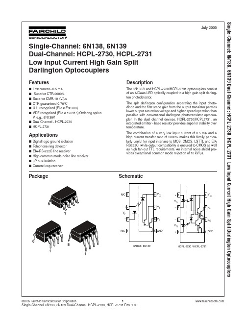
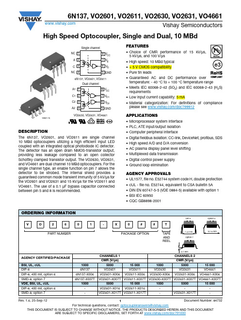
经查大量资料后,以下是目前市场上常见的高速光藕型号:100K bit/S:6N138、6N139、PS87031M bit/S:6N135、6N136、CNW135、CNW136、PS8601、PS8602、PS8701、PS9613、PS9713、CNW4502、HCPL-2503、HCPL-4502、HCPL-2530(双路)、HCPL-2531(双路)10M bit/S:6N137、PS9614、PS9714、PS9611、PS9715、HCPL-2601、HCPL-2611、HCPL-2630(双路)、HCPL-2631(双路)光耦合器的增益被称为晶体管输出器件的电流传输比 (CTR),其定义是光电晶体管集电极电流与LED正向电流的比率(ICE/IF)。
6N139S中文资料
Device
All
Min Typ** Max
1.30 1.7 1.75
Unit
V
All
5.0
20
V
Temperature coefficient of forward voltage (IF = 1.6 mA) DETECTOR Logic high output current (IF = 0 mA, VO = VCC = 18 V) Each Channel (IF = 0 mA, VO = VCC = 7 V) Each Channel Logic low supply (IF = 1.6 mA, VO = Open) (VCC = 18 V) (IF1 = IF2 = 1.6 mA, VCC = 18 V) (VO1 - VO2 = Open, VCC = 7 V Logic high supply (IF = 0 mA, VO = Open, VCC = 18 V) (IF1 = IF2 = 0 mA, VCC = 18 V) (VO1 - VO2 = Open, VCC = 7 V ** All Typicals at TA = 25°C
Device
6N139 HCPL-2731 6N139 HCPL-2731 6N138 HCPL-2730
Min
400
Typ**
1100 3500
Max
Unit
%
500
1300 2500
%
300
1300 2500 0.08 0.01 0.4 0.4
%
Logic low output voltage output voltage (Note 2)
Symbol
TSTG TOPR TSOL
6n137光耦 光隔
High Speed Optocoupler, Single and Dual, 10 MBdDESCRIPTIONThe 6N137, VO2601, and VO2611 are single channel 10 MBd optocouplers utilizing a high efficient input LED coupled with an integrated optical photodiode IC detector. The detector has an open drain NMOS-transistor output, providing less leakage compared to an open collector Schottky clamped transistor output. The VO2630, VO2631, and VO4661 are dual channel 10 MBd optocouplers. For the single channel type, an enable function on pin 7 allows the detector to be strobed. The internal shield provides a guaranteed common mode transient immunity of 5 kV/μs for the VO2601 and VO2631 and 15 kV/μs for the VO2611 and VO4661. The use of a 0.1 μF bypass capacitor connected between pin 5 and 8 is recommended.FEATURES•Choice of CMR performance of 15 kV/μs, 5 kV/μs, and 100 V/μs•High speed: 10 MBd typical •+ 5 V CMOS compatibility •Pure tin leads•Guaranteed AC and DC performance over temperature: - 40 °C to + 100 °C temperature range•Meets IEC 60068-2-42 (SO 2) and IEC 60068-2-43 (H 2S) requirements•Low input current capability: 5 mA•Material categorization: For definitions of compliance please see /doc?99912 APPLICATIONS•Microprocessor system interface •PLC, ATE input/output isolation •Computer peripheral interface•Digital fieldbus isolation: CC-link, DeviceNet, profibus, SDS •High speed A/D and D/A conversion •AC plasma display panel level shifting •Multiplexed data transmission •Digital control power supply •Ground loop eliminationAGENCY APPROVALS•UL1577, file no. E52744 system code H, double protection •cUL - file no. E52744, equivalent to CSA bulletin 5A •DIN EN 60747-5-5 (VDE 0884-5) available with option 1•BSI IEC 60950•CQC GB8898-200118921-15Notes•Stresses in excess of the absolute maximum ratings can cause permanent damage to the device. Functional operation of the device is not implied at these or any other conditions in excess of those given in the operational sections of this document. Exposure to absolute maximum ratings for extended periods of the time can adversely affect reliability.(1)Refer to reflow profile for soldering conditions for surface mounted devices (SMD). Refer to wave profile for soldering conditions for through hole devices (DIP).TRUTH TABLE (positive logic)LED ENABLEOUTPUTOn H L Off H H On L H Off L H On NC L OffNCHABSOLUTE MAXIMUM RATINGS (T amb = 25 °C, unless otherwise specified)PARAMETER TEST CONDITIONSYMBOLVALUEUNITINPUTAverage forward current (single channel)I F 20mA Average forward current (per channel for dual channel)I F 15mA Reverse input voltage V R 5V Enable input voltage V E V CC + 0.5 VV Enable input current I E 5mA Surge currentt = 100 μsI FSM 200mA Output power dissipation (single channel)P diss 35mW Output power dissipation (per channel for dual channel)P diss25mWOUTPUT Supply voltage 1 min maximumV CC 7V Output current I O 50mA Output voltageV O 7V Output power dissipation (single channel)P diss 85mW Output power dissipation (per channel for dual channel)P diss60mWCOUPLERIsolation test voltage t = 1 sV ISO 5300V RMS Storage temperature T stg - 55 to + 150°C Operating temperature T amb- 40 to + 100°C Lead solder temperature for 10 s 260°C Solder reflow temperature (1)260°CRECOMMENDED OPERATING CONDITIONSPARAMETER TEST CONDITIONSYMBOL MIN.MAX.UNIT Operating temperature T amb - 40100°C Supply voltage V CC 4.5 5.5V Input current low level I FL 0250μA Input current high level I FH 515mA Logic high enable voltage V EH 2V CC V Logic low enable voltage V EL 00.8V Output pull up resistor R L 3304K ΩFanoutR L = 1 k ΩN5-Note•Minimum and maximum values are testing requirements. Typical values are characteristics of the device and are the result of engineering evaluation. Typical values are for information only and are not part of the testing requirements.Notes•Over recommended temperature (T amb = - 40 °C to + 100 °C), V CC = 5 V, I F = 7.5 mA unless otherwise specified. All typicals at T amb = 25 °C, V CC = 5 V.(1)75 ns applies to the 6N137 only, a JEDEC registered specificationELECTRICAL CHARACTERISTICS (T amb = 25 °C, unless otherwise specified)PARAMETER TEST CONDITIONSYMBOLMIN.TYP.MAX.UNIT INPUTInput forward voltage I F = 10 mA V F 1.11.4 1.7V Reverse current V R = 5 V I R 0.0110μA Input capacitance f = 1 MHz, V F = 0 V C I 55pF OUTPUTHigh level supply current (single channel)V E = 0.5 V, I F = 0 mA I CCH 4.17mA V E = V CC , I F = 0 mAI CCH 3.36mA High level supply current (dual channel)I F = 0 mA I CCH 6.512mA Low level supply current (single channel)V E = 0.5 V, I F = 10 mA I CCL 47mA V E = V CC , I F = 10 mAI CCL 3.36mA Low level supply current (dual channel)I F = 10 mAI CCL 6.512mA High level output current V E = 2 V, V O = 5.5 V, I F = 250 μAI OH 0.0021μA Low level output voltage V E = 2 V, I F = 5 mA,I OL (sinking) = 13 mA V OL 0.20.6V Input threshold current V E = 2 V, V O = 5.5 V,I OL (sinking) = 13 mAI TH 2.45mA High level enable current V E = 2 V I EH - 0.6- 1.6mA Low level enable current V E = 0.5 VI EL - 0.8- 1.6mA High level enable voltage V EH 2V Low level enable voltageV EL0.8VSWITCHING CHARACTERISTICSPARAMETERTEST CONDITION SYMBOL MIN.TYP.MAX.UNIT Propagation delay time to high output levelR L = 350 Ω, C L = 15 pF t PLH 204875 (1)ns t PLH 100ns Propagation delay time to low output levelR L = 350 Ω, C L = 15 pF t PHL 255075 (1)ns t PHL 100ns Pulse width disortion R L = 350 Ω, C L = 15 pF |t PHL - t PLH|2.935ns Propagation delay skew R L = 350 Ω, C L = 15 pF t PSK 840ns Output rise time (10 % to 90 %)R L = 350 Ω, C L = 15 pF t r 23ns Output fall time (90 % to 10 %)R L = 350 Ω, C L = 15 pF t f 7ns Propagation delay time of enable from V EH to V EL R L = 350 Ω, C L = 15 pF,V EL = 0 V, V EH = 3 V t ELH 12ns Propagation delay time of enable from V EL to V EHR L = 350 Ω, C L = 15 pF,V EL = 0 V, V EH = 3 Vt EHL11nsFig. 1 - Single Channel Test Circuit for t PLH , t PHL , t r and t fFig. 2 - Dual Channel Test Circuit for t PLH , t PHL , t r and t fFig. 3 - Single Channel Test Circuit for t EHL , and t ELHNotes(1)For 6N137 and VO2630(2)For VO2601 and VO2631(3)For VO2611 and VO4661COMMON MODE TRANSIENT IMMUNITYPARAMETERTEST CONDITIONSYMBOL MIN.TYP.MAX.UNIT Common mode transient immunity (high)|V CM | = 10 V, V CC = 5 V, I F = 0 mA,V O(min.) = 2 V, R L = 350 Ω, T amb = 25 °C (1)|CM H |1000V/μs|V CM | = 50 V, V CC = 5 V, I F = 0 mA,V O(min.) = 2 V, R L = 350 Ω, T amb = 25 °C (2)|CM H |500010 000V/μs |V CM | = 1 kV, V CC = 5 V, I F = 0 mA,V O(min.) = 2 V, R L = 350 Ω, T amb = 25 °C (3)|CM H |15 00025 000V/μs |V CM | = 10 V, V CC = 5 V, I F = 7.5 mA,V O(max.) = 0.8 V, R L = 350 Ω, T amb = 25 °C (1)|CM L |1000V/μs|V CM | = 50 V, V CC = 5 V, I F = 7.5 mA,V O(max.) = 0.8 V, R L = 350 Ω, T amb = 25 °C (2)|CM L |500010 000V/μs |V CM | = 1 kV, V CC = 5 V, I F = 7.5 mA,V O(max.) = 0.8 V, R L = 350 Ω, T amb = 25 °C (3)|CM L |15 00025 000V/μsFig. 4 - Single Channel Test Circuit for Common Mode Transient ImmunityFig. 5 - Dual Channel Test Circuit for Common Mode Transient ImmunitySAFETY AND INSULATION RATINGSPARAMETER TEST CONDITION SYMBOL MIN.TYP.MAX.UNIT Climatic classification according to IEC 68 part 155/100/21Comparative tracking index CTI175399Peak transient overvoltage V IOTM8000V Peak insulation voltage V IORM890V Safety rating - power output P SO500mW Safety rating - input current I SI300mA Safety rating - temperature T SI175°C Creepage distance Standard DIP-87mm Clearance distance Standard DIP-87mm Creepage distance400 mil DIP-88mm Clearance distance400 mil DIP-88mm Insulation thickness, reinforced rated per BSI 609500.2mm Note•As per IEC 60747-5-5, §7.4.3.8.2, this optocoupler is suitable for “safe electrical insulation” only within the safety ratings. Compliance with the safety ratings shall be ensured by means of prodective circuits.TYPICAL CHARACTERISTICS (T amb = 25 °C, unless otherwise specified)Fig. 6 - Forward Voltage vs. Ambient Temperature Fig. 7 - Forward Voltage vs. Forward Current Fig. 8 - Reverse Current vs. Ambient TemperatureFig. 9 - Low Level Supply Current vs. Ambient Temperature Fig. 10 - High Level Supply Current vs. Ambient Temperature Fig. 11 - Input Threshold On Current vs. Ambient TemperatureFig. 12 - Input Threshold Off Current vs. Ambient Temperature Fig. 13 - Low Level Output Voltage vs. Ambient Temperature Fig. 14 - Low Level Output Current vs. Ambient Temperature Fig. 15 - High Level Output Current vs. Ambient Temperature Fig. 16 - Output Voltage vs. Forward Input CurrentFig. 17 - Propagation Delay vs. Ambient TemperatureFig. 18 - Propagation Delay vs. Forward CurrentFig. 19 - Pulse Width Distortion vs. Ambient Temperature Fig. 20 - Pulse Width Distortion vs. Forward CurrentFig. 21 - Rise and Fall Time vs. Ambient Temperature Fig. 22 - Rise and Fall Time vs. Forward CurrentFig. 23 - Enable Propagation Delay vs. Ambient TemperaturePACKAGE DIMENSIONS in millimetersPACKAGE MARKINGNotes•Option 1 and VDE logo are only marked on option 1 parts.•Tape and reel suffix (T) is not part of the package marking.Legal Disclaimer Notice VishayDisclaimerALL PRODU CT, PRODU CT SPECIFICATIONS AND DATA ARE SU BJECT TO CHANGE WITHOU T NOTICE TO IMPROVE RELIABILITY, FUNCTION OR DESIGN OR OTHERWISE.Vishay Intertechnology, Inc., its affiliates, agents, and employees, and all persons acting on its or their behalf (collectively,“Vishay”), disclaim any and all liability for any errors, inaccuracies or incompleteness contained in any datasheet or in any other disclosure relating to any product.Vishay makes no warranty, representation or guarantee regarding the suitability of the products for any particular purpose or the continuing production of any product. To the maximum extent permitted by applicable law, Vishay disclaims (i) any and all liability arising out of the application or use of any product, (ii) any and all liability, including without limitation special, consequential or incidental damages, and (iii) any and all implied warranties, including warranties of fitness for particular purpose, non-infringement and merchantability.Statements regarding the suitability of products for certain types of applications are based on Vishay’s knowledge of typical requirements that are often placed on Vishay products in generic applications. Such statements are not binding statements about the suitability of products for a particular application. It is the customer’s responsibility to validate that a particular product with the properties described in the product specification is suitable for use in a particular application. Parameters provided in datasheets and/or specifications may vary in different applications and performance may vary over time. All operating parameters, including typical parameters, must be validated for each customer application by the customer’s technical experts. Product specifications do not expand or otherwise modify Vishay’s terms and conditions of purchase, including but not limited to the warranty expressed therein.Except as expressly indicated in writing, Vishay products are not designed for use in medical, life-saving, or life-sustaining applications or for any other application in which the failure of the Vishay product could result in personal injury or death. Customers using or selling Vishay products not expressly indicated for use in such applications do so at their own risk. Please contact authorized Vishay personnel to obtain written terms and conditions regarding products designed for such applications. No license, express or implied, by estoppel or otherwise, to any intellectual property rights is granted by this document or by any conduct of Vishay. Product names and markings noted herein may be trademarks of their respective owners.Material Category PolicyVishay Intertechnology, Inc. hereby certifies that all its products that are identified as RoHS-Compliant fulfill the definitions and restrictions defined under Directive 2011/65/EU of The European Parliament and of the Council of June 8, 2011 on the restriction of the use of certain hazardous substances in electrical and electronic equipment (EEE) - recast, unless otherwise specified as non-compliant.Please note that some Vishay documentation may still make reference to RoHS Directive 2002/95/EC. We confirm that all the products identified as being compliant to Directive 2002/95/EC conform to Directive 2011/65/EU.Vishay Intertechnology, Inc. hereby certifies that all its products that are identified as Halogen-Free follow Halogen-Free requirements as per JEDEC JS709A standards. Please note that some Vishay documentation may still make reference to the IEC 61249-2-21 definition. We confirm that all the products identified as being compliant to IEC 61249-2-21 conform to JEDEC JS709A standards.。
6N137中文资料
6N137中文资料概述6N137是一款具有高输出截止速度和高电流传输能力的光耦合器。
其内部结构包括一个红外发光二极管和一个高速光敏二极管。
6N137的主要特点是具有高速响应、低功耗、免磁屏蔽、高隔离电压和长寿命等优点。
这些特点使得6N137广泛应用于各种测量、控制、通信等领域。
功能特点•具有高达10 Mbps的数据传输速度。
•高达1 mA的输出电流。
•高达10 kV的隔离电压。
•通过红外光传输信号,具有免磁屏蔽的优点。
•宽工作温度范围,可在-40℃至+100℃的温度下正常工作。
•长寿命,可达10万小时以上。
引脚功能6N137一共有8个引脚,其中1号和2号为光敏输入端口,3号为非常重要的共阳极输出端口,其余引脚作为电源与反馈引脚。
下图为6N137的引脚示意图:1. Anode (A)2. Anode (A)3. Cathode (-), Output (O)4. Ground5. Vcc (+)6. Feedback7. NC (Not Connected)8. NC (Not Connected)应用场景由于6N137具有高速响应、低功耗、高隔离电压和长寿命等优点,因此其应用范围非常广泛,以下是其常见应用场景:工业控制6N137可以作为输出接口,用于将PLC(可编程逻辑控制器)隔离。
由于工业控制设备需要承受更高的工作环境和噪声,所以6N137高隔离能力和免磁屏蔽的特点可以保证其信号的可靠性。
数字信号传输由于6N137具有高达10 Mbps的数据传输速度,可用于数字信号隔离与传输,广泛应用于数码显示、传感器接口电路等。
模拟信号隔离6N137也可用于模拟信号隔离,将输入信号隔离后,输出的信号不会受到过渡现象的干扰,保证输出的准确性。
其他领域6N137还可以应用于电力系统、通讯系统中,作为隔离器和信号放大器,以提高系统的稳定性和准确性。
总结以上就是6N137中文资料的介绍,6N137是一款性能稳定、速度快、隔离电压高、寿命长的光耦合器,被广泛应用于控制、测量、通信和电力等领域。
光耦的应用
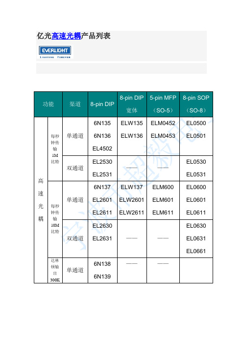
功能渠道8-pin DIP8-pin DIP宽体5-pin MFP(SO-5)8-pin SOP(SO-8)高速光耦每秒钟传输1M比特单通道6N1356N136EL4502ELW135ELW136ELM0452ELM0453EL0500EL0501 双通道EL2530EL2531————EL0530EL0531每秒钟传输10M比特单通道6N137EL2601EL2611ELW137ELW2601ELW2611ELM600ELM601ELM611EL0600EL0601EL0611 双通道EL2630EL2631 ————EL0630EL0631EL0661 达林顿输出300K单通道6N1386N139————亿光的高速光耦一般应用在电源上,具体应用在放点等离子,固态继电器,工业测量机,调制器,电话,空调控制板,可编程逻辑控制器等等。
电源工作渠道固态继电器(SSR)Photo TriacEL302X,EL305X,EL304X,EL306X,EL308XELM302X,ELM305X,ELM304X,ELM306X,ELM308X高速光耦应用在空调标准EL817,EL357N-G 空调机应用到的光耦驱动EL3120高速光耦应用在驱动电源标准EL357N-G,EL3H7-G 驱动器应用到的光耦高速6N136,EL0500高速光耦的应用末端设备电话交换系统so8封装晶体管末端设备电机驱动逆变器/伺服系统栅极驱动器末端设备仪表控制/工业网络缝纫机串行总线接口隔离建议的使用设备:8-Pin DIP:6N135,6N136,,EL2503 8-Pin SOP:EL0500,EL0501总线网络描述·总线接口隔离·隔离控制器和分析设备(I/O,,伺服电机,控制板,流出物处理元件)应用·工厂自动化网络(总线接口,总线,CC-LINK)建议的使用设备:5-pin SOP:ELMO452,ELMO4538-pin DIP:EL2502,EL25038-pin SOP:EL0500,EL0501数据传输框图应用:·RS485和RS-422 的隔离接口·I²C的隔离接口建议的使用设备:5-pin SOP:ELM600,ELMO601,ELM06118-pin DIP:EL2601,EL26118-pin SOP:EL0500,EL0501,EL0601,EL0611PLC输入/输出(可编程逻辑控制器)通讯(面板与面板之间)建议的使用设备:5-pin SOP:ELM601,ELM6118-pin SOP:EL0601,EL0611,EL0630,EL0631电机控制描述·电流隔离电机线和控制集成电路·电机驱动控制的高速开关应用·IPM驱动/变频驱动建议的使用设备:5-pin SOP:ELM452,ELM453 8-pin DIP:EL0452,EL0453 8-pin SOP:EL0452,EL0453筑控设备描述:·通信线路之间的隔离室控制器·电机驱动控制的高速开关应用:·数据通信·IPM驱动/变频驱动建议的使用设备:5-pin SOP:ELM452,ELM4538-pin SOP:EL0630,EL0631,EL0611。
亿光的光耦el817的工作寿命评估方式

亿光的光耦el817的工作寿命评估方式光耦是一种将输入光信号和输出电信号进行电光转换的器件,广泛应用于各种电子设备中。
其中,亿光的光耦型号el817是一种常用的光耦产品。
在评估el817的工作寿命时,可以考虑以下几个方面:光电转换性能、环境因素、温度、电器荷电量、加电击波和终端压力。
首先,光电转换性能是评估el817工作寿命的重要指标之一。
光电转换性能包括光耦的转换速度、滞后时间和线性度等方面。
在实际应用中,光耦的转换速度要求越高,生命周期就越短。
因此,使用el817作为光耦时,需要根据具体需求选择合适的型号,并根据其提供的转换速度等参数进行评估。
其次,环境因素也会对el817的工作寿命产生影响。
环境因素主要包括湿度、光照强度和尘埃等。
湿度过高会导致光耦内部元件的腐蚀,从而降低工作寿命;光照强度过高会导致光耦内部元件的老化,同样会缩短工作寿命;而尘埃对光耦的外部结构形成阻隔,影响光信号的输入和输出,进而影响光耦的转换性能和工作寿命。
此外,温度对el817的工作寿命也有重要影响。
温度过高会使光耦内部元件的粘结材料老化,导致光电转换性能下降,从而缩短工作寿命。
因此,在设计电路时,需要根据实际环境温度,选择合适的散热措施,以保证el817在合适的温度范围内工作。
同时,电器荷电量也是评估el817工作寿命的重要因素之一。
电器荷电量是指光耦元器件上积累的电荷量,过高的电器荷电量会导致静电放电现象,进而对光电转换性能和工作寿命造成不可逆的损害。
此外,加电击波也是一个重要的评估因素。
在实际应用中,电路开关和继电器的加电冲击会影响光耦的工作寿命。
因此,在电路设计中,需要考虑合适的保护电路来减小电路开关对光耦产生的冲击,从而提高工作寿命。
最后,终端压力也是影响el817工作寿命的因素之一。
终端压力过大,会使光耦内部元件的结构变形,进而影响光电转换性能和工作寿命。
因此,在应用中需要注意处理好终端压力,避免对光耦造成不可逆的损害。
- 1、下载文档前请自行甄别文档内容的完整性,平台不提供额外的编辑、内容补充、找答案等附加服务。
- 2、"仅部分预览"的文档,不可在线预览部分如存在完整性等问题,可反馈申请退款(可完整预览的文档不适用该条件!)。
- 3、如文档侵犯您的权益,请联系客服反馈,我们会尽快为您处理(人工客服工作时间:9:00-18:30)。
8 PIN DIP LOW INPUT CURRENT HIGH GAIN SPLIT DARLINGTON PHOTOCOUPLER 6N138 6N139Features• High current transfer ratio–2000% typical• High isolation voltage between input and output (Viso=5000 Vrms ) • Guaranteed performance from 0°C to 70°C • Pb free and RoHS compliant. • UL approved (No. 214129) • VDE approved (No. 132249) • SEMKO approved • NEMKO approved • DEMKO approved • FIMKO approved•CSA approved (No. 2037145)DescriptionThe 6N138 and 6N139 devices each consists of an infrared emitting diode, optically coupled to a high gain split Darlington photo detector. They provide extremely high current transfer ratio between input and output, withaccess to a base terminal to adjust the gain bandwidth.These devices are packaged in an 8-pin DIP package and available in wide-lead spacing and SMD options.Applications• Digital logic ground isolation • RS-232C line receiver• Low input current line receiver • Microprocessor bus isolation • Current loop receiverAbsolute Maximum Ratings (Ta=25)℃Parameter Symbol Rating UnitInput Forward current I F20 mA Peak forward current(50% duty, 1ms P.W)I FP40 mA Peak transientcurrent(≤1µs P.W,300pps)I Ftrans 1 A Reverse voltage V R 5 V Power dissipation P IN45 mWOutput Power dissipation P O100 mW Output current IO 60 mA Emitter-BaseReverse VoltageVER 0.5 V Output voltage6N138V O-0.5 to 7-0.5 to 18V6N139Supply voltage6N138V CC-0.5 to 7-0.5 to 18V6N139Isolation voltage *1V ISO5000 V rmsOperating temperature TOPR-40 ~ +85 °C Storage Temperature T STG-55 ~ +125 °CSoldering temperature *2T SOL260 °CNotes:*1 AC for 1 minute, R.H.= 40 ~ 60% R.H. In this test, pins 1, 2, 3, 4 are shorted together, and pins 5, 6, 7, 8 are shorted together. *2 For 10 secondsElectrical Characteristics (T A=0 to 70°C unless specified otherwise)InputParameter Symbol Min. Typ. Max. Unit Condition Forward voltage V F- 1.3 1.7 V I F = 1.6mAReverse Voltage V R 5.0 - - V I R = 10µA, T A=25°C Temperaturecoefficient of forwardvoltage∆V F/∆T A- -1.8 - mV/°C I F =1.6mA OutputParameter Symbol Min Typ. Max. Unit ConditionLogic High Output Current 6N138I OH- 0.01 100µA I F=0mA, V O=V CC=18V 6N139 - - 250Logic Low Supply Current 6N138I CCL- 0.6 1.5 mAI F=1.6mA, V O=Open,V CC=18V6N139Logic High Supply Current 6N138I CCH- 0.05 10 µAI F=0mA, V O=Open,V CC=18V6N139Transfer Characteristics (T a=0 to 70°C unless specified otherwise, Vcc=4.5V) Parameter Symbol Min Typ. Max. Unit ConditionCurrent Transfer Ratio 6N139CTR400 2500 -%I F= 0.5mA, V O= 0.4V,V CC=4.5V500 2000 - IF= 1.6mA, V O= 0.4V,V CC=4.5V6N138 300 2000 -Logic Low Output Voltage 6N139V OL- 0.05 0.4VI F = 0.5mA, I O = 2mA,V CC=4.5V- 0.09 0.4I F = 1.6mA, I O = 8mA,V CC=4.5V- 0.12 0.4I F = 5mA, I O = 15mA,V CC=4.5V- 0.17 0.4I F = 12mA, I O = 24mA,V CC=4.5V6N138 - 0.06 0.4I F = 1.6mA, I O =4.8mA, V CC=4.5VSwitching Characteristics (T a=0 to 70°C unless specified otherwise, Vcc=5V) Parameter Symbol Min Typ. Max. Unit ConditionPropagatio n Delay Time to Logic Low (Fig. 13) 6N139TPHL- 5 25µsI F= 0.5mA , R L=4.7kΩ,T A=25°C- - 30 I F= 0.5mA , R L=4.7kΩ- 0.2 1 I F= 12mA , R L=270Ω,T A=25°C- - 2 I F= 12mA , R L=270Ω6N138- 1.4 10 I F= 1.6mA , R L=2.2kΩ,T A=25°C- - 15 I F= 1.6mA , R L=2.2kΩPropagatio n Delay Time to Logic High (Fig. 13) 6N139TPLH- 16 60µsI F= 0.5mA , R L=4.7kΩ,T A=25°C- - 90 I F= 0.5mA , R L=4.7kΩ- 1.7 7I F= 12mA , R L=270Ω,T A=25°C- - 10 I F= 12mA , R L=270Ω6N138- 8 35 I F= 1.6mA , R L=2.2kΩ,T A=25°C- - 50 I F= 1.6mA , R L=2.2kΩCommon ModeTransient Immunity at Logic High(Fig. 14) *3CM H1,000 - - V/µsI F= 0mA ,V CM=10Vp-p,R L=2.2KΩ, T A=25°CCommon ModeTransient Immunity at Logic Low(Fig. 14) *3CM L1,000 - - V/µsI F= 1.6mA ,V CM=10Vp-p,R L=2.2KΩ, T A=25°C* Typical values at T a = 25°CTypical Electro-Optical Characteristics CurvesFig. 14 Common Mode Transient Immunity Test Circuit and WaveformNote:*3 Common mode transient immunity in logic high level is the maximum tolerable (positive) dVcm/dt on the leading edge of the common mode pulse signal VCM, to assure that the output will remain in a logic high state (i.e., VO > 2.0V).Common mode transient immunity in logic low level is the maximum tolerable (negative) dVcm/dt on the trailing edge of the common mode pulse signal, VCM, to assure that the output will remain in a logic low state (i.e., VO < 0.8V).+5VVoI V O 5VPLH PHL VOrder InformationPart Number6N13XY(Z)-VNoteX = Part No. (X = 8 or 9)Y = Lead form option (S, S1, M or none)Z = Tape and reel option (TA, TB or none).V = VDE (optional)Option Description Packing quantity None Standard DIP-8 45 units per tubeM Wide lead bend (0.4 inch spacing) 45 units per tubeS (TA) Surface mount lead form + TA tape & reel option 1000 units per reelS (TB) Surface mount lead form + TB tape & reel option 1000 units per reelS1 (TA) Surface mount lead form (low profile) + TA tape & reel option 1000 units per reelS1 (TB) Surface mount lead form (low profile) + TB tape & reel option 1000 units per reelPackage Dimension (Dimensions in mm) Standard DIP TypeOption M TypeOption S TypeOption S1 TypeRecommended pad layout for surface mount leadformDevice MarkingNotesEL denotes EVERLIGHT6N138 denotes Device NumberY denotes 1 digit Year codeWW denotes 2 digit Week codeV denotes VDE (Optional)EL6N138YWWVTape & Reel Packing SpecificationsDimension No. A B Do D1 E F Dimension(mm) 10.4±0.1 10.0±0.1 1.5+0.1/-01.5±0.25/-01.75±0.1 7.5±0.1 Dimension No. Po P1 P2 t W K Dimension(mm)4.0±0.112.0±0.12.0±0.050.4±0.0516.0±0.3/4.5±0.1Option TBDirection of feed from reelPrecautions for Use1. Soldering Condition1.1 (A) Maximum Body Case Temperature Profile for evaluation of Reflow ProfileNote: Reference: IPC/JEDEC J-STD-020DPreheatTemperature min (T smin) 150 °CTemperature max (T smax) 200°CTime (T smin to T smax) (t s) 60-120 secondsAverage ramp-up rate (T smax to T p) 3 °C/second maxOtherLiquidus Temperature (T L) 217 °CTime above Liquidus Temperature (t L)60-100 secPeak Temperature (T P) 260°CTime within 5 °C of Actual Peak Temperature: T P - 5°C 30 sRamp- Down Rate from Peak Temperature 6°C /second max.Time 25°C to peak temperature 8 minutes max.Reflow times 3 times.DISCLAIMER1. Above specification may be changed without notice. EVERLIGHT will reserve authority on material change forabove specification.2. When using this product, please observe the absolute maximum ratings and the instructions for using outlined inthese specification sheets. EVERLIGHT assumes no responsibility for any damage resulting from use of the product which does not comply with the absolute maximum ratings and the instructions included in these specification sheets.3. These specification sheets include materials protected under copyright of EVERLIGHT corporation. Please don’treproduce or cause anyone to reproduce them without EVERLIGHT’s consent.。