LNA_ design (设计实例)
!LNAdesign

射频低噪声放大器设计初探一.射频低噪声放大器指标及其在无线通信系统中的作用低噪声放大器在无线通信接收系统中位于双工器后的第一级,作为接收机的重要组成部分,低噪放的主要功能是对接收微弱信号的放大,尽量减少噪声的增加,从而保证系统在极低功率电平下的信噪比恶化量最小。
另外低噪放还必须保证在强信号接收的情况下保持较好的线性度,保证系统不受到非线性失真的影响。
下面对通信系统对低噪声放大器各项指标的要求作一下简要的介绍:1.噪声系数NF这项指标应该说是设计目标中最重要的一项,由噪声系数的级联公式可知,作为系统的最前端对整个系统的影响是最大的,而噪声系数直接影响接收机的灵敏度,下面举例说明如何根据系统要求确定接收机和低噪放噪声系数指标:以CDMA手机为例:IS-98A/95B 及一些过度性标准中规定手机接收灵敏度电平为-104dBm(天线口接收到的总功率Iˆ or此时业务信道功率为-119.6dBm)灵敏度电平时的误帧率FER 不超过0.5%。
影响接收机灵敏度的干扰有两个一个是输入高斯白噪声记为No 另一个主要干扰为发射机的功率泄漏记为Ntx。
No 的大小由接收机噪声系数决定,Ntx 则取决于发射机的噪声底和前端双工器的抑制特性,典型的功放输出噪声底在接收频段为-135dBm/Hz 假定双工器提供43dB的抑制可以计算得NTx为-178dBm/Hz。
IS-98A给出[Eb/Nt]应不小于4.5dB,测试参考灵敏度时的信号速率为9.6K,根据信号速率可计算出当前的处理增益Gp 为10*Log(12288/96)=21.1dB 我们可以有下面的公式计算出当前的整个噪声功率:上式中S 表示业务信道功率Ntl,包括两部分一部分为No,等于[KTB]+NF=-113dBm+NF,另一部分为发射机功率泄漏等于Ntx+[B]=-117dBm,(注K 是Boltzman 常数B,等于1.2288MHz,T等于290K),根据这些数值做进一步推导可得到NF 应小于9.8dB 在实际设计时建议放2dB余量以克服其他损耗如处理增益不十分理想等考虑双工器损耗为4dB,则接收机噪声系数为3.8dB(不包括双工器),根据仿真结果在蜂窝频段LNA 的噪声系数应小于2dB,在PCS频段LNA的噪声系数应小于2.3dB。
LNA仿真实验教程
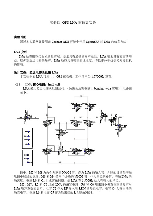
实验四 GPS LNA前仿真实验实验目的通过本实验掌握使用在Cadence ADE环境中使用SpectreRF对LNA的仿真方法LNA介绍LNA处在射频接收机的最前端,要求具有最低的噪声系数。
LNA需要具有较高的增益,以抑制后级电路的噪声。
LNA还应具备较高的线性度,降低带外干扰信号对接收机的影响。
设计实例:源级电感负反馈LNA本实验中的LNA可应用于GPS接收机,工作频率为1.575GHz左右。
(1) LNA核心电路:lna2_cellLNA采用源级电感负反馈结构,(源级负反馈电感由bonding wire实现),电路图如下。
图中,M0和M1为两个并联的NMOS管,作为LNA的输入管,并联的目的是增加版图中联线的宽度。
M3和M4是两个并联的NMOS管,作为共源共栅管,增加LNA的隔离度。
电感L0和C1组成谐振网络,是LNA在1.57GHz处具有较大的增益。
M5、M7、R0和C0组成LNA的偏置电路,R0和C0用来减小偏置电路的噪声对LNA噪声系数的影响。
电容C2作为RF输入端RFIN的隔直电容。
电容C4为输出端的隔直电容。
电感L3和电容C5作为输出端的L型匹配电路。
为了防止其它电路的噪声通过地线串扰影响LNA的噪声系数,在电路中设置了3种地线:GND1为主电路的地、GND2为其它电路的地线,SUB为所有器件衬底的接地点。
(2) 考虑各接出点的ESD以后的电路图lna2_cell_WPAD每个PIN都需要考虑ESD,本实验中,我们采用TSMC提供的标准RFIO作为各PIN的ESD器件,LNA一共有7个IO,所以共有7个ESD器件。
其中LNA的电源采用电源ESD器件(PVDD3AC);SUB引出采用地线ESD器件(PVSS3AC);RFIN、RFOUT 采用最小寄生电容的ESD器件PDB1AC;其余的IBIAS和GND2、GND1采用PDB3AC.(3)各种ESD器件的电路原理和在版图中的连接方法PDB1AC、PDB3AC、PVSS3AC和PVDD3AC都在tsmc18io库中。
2.5GHz WiMAX低噪声放大器(LNA)设计

关键字:低噪声放大器LNA ATF-551M4负反馈放大器WiMAX又称为802.16无线城域网,是又一种为企业和家庭用户提供“最后一英里”的宽带无线连接方案。
因其能提供高速的数据业务以及对3G可能构成的威胁,使WiMAX在最近一段时间备受业界关注。
低噪声放大器是接收机的重要组成部分,它对降低接收链路的噪声系数(NF),提高整个接收机的灵敏度起着至关重要的作用。
由于它位于接收机的最前端,所以要求它具有很小的噪声系数。
为了抑制后级元件对噪声系数的影响,又要求它具有合适的增益。
为了满足2.5GHZ WiMAX应用,要求该低噪声放大器在工作频段2.49~2.69GHz内能有>14dB的增益,<1dB的噪声系数。
为了降低接收机成本,该低噪声放大器基于低廉的FR4板材,并采用Avago的一款E-PHEMT(增强型伪高电子迁移率晶体管)ATF-551M4设计,ATF-551M4价格较ATF-54143更为便宜,同时ATF-551M4具有更低的漏级偏置电流,能够有效降低接收机功耗。
输入匹配电路设计为了满足系统设计要求的噪声系数,增益,同时获得好的线性度,选取该器件沟道电流(Ids)为30mA,漏极到源极电压为3V,根据ATF-551M4的datasheet3,该E-pHEMT晶体管具有如下典型值:2.5GHz S11=0.690∠-131.0°,3.0GHz S11=0.668∠-146.0°,2.4GHz F min= 0.45 F opt=0.33∠54°R n/50=0.09。
3.0GHz F min= 0.52 F opt=0.26∠79°R n/50=0.09。
可以看出最佳输入匹配点S11*与最小噪声匹配点F opt相差比较远,所以我们不可能同时获得较好的噪声系数和输入回损。
实际上,由于LNA离天线比较近,为了保证天线口良好的驻波比,我们对低噪声放大器的输入回损要求比较高,因此,需将低噪声放大器的输入匹配到最佳匹配点S11*。
《LNA的设计》PPT课件

微带电路拓扑结构的选择原则
(1)微波的高频段,比如工作频率在X波段或更高,宜选用微 带阻抗跳变式的阻抗变换器类,
(2)对于微波的低频段,例如S波段或更低端,宜选用分支微 带结构。
(3)微波管输入阻抗为容性时,此时s11处在史密斯圆图下半平 面,匹配电路第1个微带元件宜用电感性微带单元;反之,
当s11处在史密斯圆图上半平面时,宜用电容性微带单元。
共扼增益、单向化增益等。
对于实际的低噪音放大器,功率增益通常是指信源和负载都是
50Ω标准阻抗情况下实测的增益。
实际测量时,常用插入法,即用功率计先测信号源能给出的功
率 P1;再把放大器接到信源上,用同一功率计测放大器输出功率 P2, 功率增益就是
G P2 P1
低噪声放大器都是按照噪声最佳匹配进行设计的。噪声最佳匹
低噪声放大器主要指标是噪声系数,所以输入匹配电 路是按照噪声最佳来设计的,其结果会偏离驻波比最 佳的共扼匹配状态,因此驻波比不会很好。
此外,由于微波场效应晶体或双极性晶体管,其增益 特性大体上都是按每倍频程以6dB规律随频率升高而 下降,为了获得工作频带内平坦增益特性,在输入匹 配电路和输出匹配电路都是无耗电抗性电路情况下, 只能采用低频段失配的方法来压低增益,以保持带内 增益平坦,因此端口驻波比必然是随着频率降低而升 高。
式中,NF 为微波部件的噪声系数;
Sin,Nin 分别为输入端的信号功率和噪声功率; Sout,Nout 分别为输出端的信号功率和噪声功率。 噪声系数的物理含义是:信号通过放大器之后,由于放大器 产生噪声,使信噪比变坏;信噪比下降的倍数就是噪声系数。
通常,噪声系数用分贝数表示,此时
NF (dB) 10 lg( NF )
此外由于微波场效应晶体或双极性晶体管其增益特性大体上都是按每倍频程以6db规律随频率升高而下降为了获得工作频带内平坦增益特性在输入匹配电路和输出匹配电路都是无耗电抗性电路情况下只能采用低频段失配的方法来压低增益以保持带内增益平坦因此端口驻波比必然是随着频率降低而升放大器的稳定性放大器的稳定性当放大器的输入和输出端的反射系数的模都小于管源阻抗和负载阻抗如何网络都是稳定的称为绝对稳定
RF Circuit design(Topic 12)LNA

福州大学通信工程系 许志猛
TOPIC 12
主要内容
有源二端口网络的噪声参量 低噪声放大器的设计方法
设计实例
等驻波比圆
设计实例
宽带放大器
频率补偿网络 平衡放大器设计 负反馈电路
LNA放大器
有源网络噪声参数一般表示式
噪声来源:BJT
热噪声 散粒噪声
2 enb 4kTrb f '
2 ine 2qIe f
2 inc 2qIc f
2 in 2qIc f F ( f )
(发射极) (集电极) (分配)
f h 0.04I c rb f T
2
闪烁(1/f)噪声
最小噪声系数 NFmin 1 h(1 1 2 / h )
FET
2 i nd 4kTf g m 0 P 沟道热噪声 2 2 ing 4kT f 2C gs / g m 0 R 栅感应噪声 谷际散射与高场扩散噪声 闪烁噪声 f 2 NF 1 2 PR ( 1 C ) 最小噪声系数 min f
GS
1
I
2
Gopt
GS
R
Fk 4dB
Gopt 0.89550 Rn 20.1 Fmin 0.6dB
噪声系数圆的性质
在等噪声系数圆上各点的Γs值不同,但可得相同的 Fk值。 把等噪声系数圆和稳定判别圆画在同一圆图上时, 对于潜在不稳定情况,可以避开不稳定区而选取稳 定区内的Γs值,以满足同样Fk的要求。 如果 Γopt 落在不稳定区,则说明最小噪声系数一般 不能实现。 在圆图上还可画出Γs平面上等功率增益圆,选择时, 可利用等F圆和等GA圆来兼顾噪声和增益的要求。
一篇有关LNA设计的优秀硕士论文
引言近几十年来,微波器件的飞速发展,如双级晶体管(BJT)、结型场效应管(JFET)的发明,以及砷化钾肖特基势垒栅场效应管(GaAs MES FET)的研制成功。
这些成功,使得微波固态电路随之也发生了飞速的进步。
由于80年代初的先进工艺,使得级间线条尺寸缩小到了亚微米级,又一次大大提高了了工作频率。
随后异质结双级晶体管(HBT),高电子迁移率晶体管(HEMT),也相继研制成功。
目前这些新的器件的工作频率已经进入了毫米波段,HEMT多用于微波低噪声放大器,现在国外已研制出毫米波单片集成电路,HBT的应用不仅可作微波功放、微波振荡器、微波开关,还可作分频器,模数变换、高速逻辑电路等,预测将来微波集成电路必然有着跟迅速的发展。
微波基本知识及课题背景分米波10-----1分米特高频(UHF)300-----3000 Hz 微波厘米波10-----1厘米超高频(SHF)3000-----30000Hz毫米波10-----1毫米极高频(EHF)30000-----300000Hz(贴图)其简单工作过程是:利用天线将从空中接受的微弱电磁波变为无调电流,经过可调谐的高频放大器选择出所需接收的信号,并同时放大信号。
放大后的高频已调信号与本振振荡器的频率相混频,变为频率较低而且固定的中频已调信号,经过中频放大以后,又检波器检出原来的调制信号,在经低频放大器放大去推动终端设备。
我的课题即是设计一个中频放大器。
中频放大器是一种频带较宽的谐振放大器。
他的主要作用是放大中频已调信号。
他与高频放大器相同之处是:二者均采用谐振回路做负载。
其差异有二:一是由于削弱邻近信号的干扰是中放的任务之一,故而中放具有接近矩形的理想谐振曲线。
二是中放具有工作频率固定与级数多两个特点。
因而中放由多级固定调谐的小信号谐振放大器组成。
高频放大器,中频放大器,其主要任务是在很多干扰和信号中选择出所需的信号加以放大,由于他们的输出信号的频率与输入信号的频率相同,因此,这些部分是接收机的线性部分。
射频射频LNA设计
《射频集成电路设计》课程设计报告LNA的设计和仿真专业:集成电路班级:电子0604学号:200681131姓名:高丕龙LNA的设计和仿真一.实验目的:1.了解低噪声放大器的工作原理及设计方法。
2.学习使用ADS软件进行微波有源电路的设计,优化,仿真。
3.掌握低噪声放大器的制作及调试方法。
二.原理简介1.低噪声放大器低噪声微波放大器(LNA)已广泛应用于微波通信、GPS接收机、遥感遥控、雷达、电子对抗、射电天文、大地测绘、电视及各种高精度的微波测量系统中,是必不可少的重要电路。
LNA是射频接收机前端的主要部分,它主要有以下四个特点:首先,它位于接收机的最前端,这就要求它的噪声系数越小越好。
为了抑制后面各级噪声对系统的影响,还要求有一定的增益,但为了不使后面的混频器过载,产生非线性失真,它的增益又不宜过大。
放大器在工作频段内应该是稳定的。
其次,它所接受的信号是很微弱的,所以低噪声放大器必定是一个小信号放大器。
而且由于受传输路径的影响,信号的强弱又是变化的,在接受信号的同时又可能伴随许多强干扰信号输入,因此要求放大器有足够的线型范围,而且增益最好是可调节的。
再次,低噪声放大器一般通过传输线直接和天线或者天线滤波器相连,放大器的输入端必须和他们很好的匹配,以达到功率最大传输或者最小的噪声系数,并保证滤波器的性能。
最后,它应具有一定的选频功能,抑制带外和镜像频率干扰,因此它一般是频带放大器。
LNA低噪声放大器的主要指标如下:1)工作频率与带宽2)噪声系数3)增益4).放大器的稳定性5)输入阻抗匹配6)端口驻波比和反射损耗在设计较高的频段低噪声放大器,通常选用场效应管FET和高电子迁移率晶体管(HEMT)。
影响放大器噪声系数的因素除了与所选用的选用元器件有关外,电路的拓扑结构是否合理也是非常重要的。
放大器的噪声系数和信号源的阻抗有关,放大器存在着最佳的信号源阻抗Zso,此时,放大器的噪声系数应该是最小的,所以放大器的输入匹配电路应该按照噪声最佳来进行设计,也就是根据所选晶体管的Гopt来进行设计。
lna设计实例

以下是一个LNA(低噪声放大器)设计实例:
1. 确定设计要求:首先,确定LNA的设计要求,包括增益、噪声系数、稳定性、线性度等参数。
2. 选择合适的工艺和器件:根据设计要求,选择合适的工艺和器件。
例如,可以选择CMOS工艺或GaAs工艺,以及相应的晶体管器件。
3. 确定电路结构:根据设计要求和选择的工艺和器件,确定LNA的电路结构。
一般来说,LNA可以采用共源共栅结构或分布式结构等。
4. 进行阻抗匹配:在进行LNA设计时,需要进行阻抗匹配以减小反射和失配损耗。
可以使用Smith圆图或其他工具进行阻抗匹配。
5. 进行噪声和增益优化:在完成阻抗匹配后,需要进行噪声和增益优化。
可以通过调整电路参数、选择合适的器件、优化电源电压等方式来优化噪声和增益。
6. 进行稳定性分析:在进行LNA设计时,需要进行稳定性分析以避免振荡。
可以通过计算稳定性系数、观察仿真结果等方式进行稳定性分析。
7. 进行版图设计:在完成上述步骤后,可以进行版图设计。
可以使用专业软件进行版图设计,包括电路图绘制、元件封装、布线等。
8. 进行测试和验证:完成版图设计后,需要进行测试和验证以验证设计的正确性和性能。
可以使用测试设备进行测试,并记录测试结果进行分析和改进。
需要注意的是,LNA设计是一个复杂的过程,需要综合考虑多个因素。
因此,在进行LNA设计时,建议参考相关文献、资料和经验,并进行多次仿真和测试以验证设计的正确性和性能。
- 1、下载文档前请自行甄别文档内容的完整性,平台不提供额外的编辑、内容补充、找答案等附加服务。
- 2、"仅部分预览"的文档,不可在线预览部分如存在完整性等问题,可反馈申请退款(可完整预览的文档不适用该条件!)。
- 3、如文档侵犯您的权益,请联系客服反馈,我们会尽快为您处理(人工客服工作时间:9:00-18:30)。
ECSE6967-RFIC Design Fall2005Assignment_3 (Due Friday 23th)Make sure to state your assumptions if they are not given in the questions.1. The LNA Design is the same as in the last problem in the class tutorial on LNAs (You can compare the hand calculated and simulated results!!). The component values are relatively close to hand calculation. Only small changes have been done to enhance the gain and Noise Figure of single ended source degenerated LNA.To characterize the LNA following figure of merits are usually measured.1. Power Consumption and Supply Voltage2. Gain3. Noise4. Input and Output Impedance Matching5. Reverse Isolation6. Stability7. LinearityWe will use S-Parameters (SP), Periodic Steady State Analysis (PSS), Periodic AC (PAC) and Pnoise analysis available in SpectreRF simulator to simulate above parameter of LNA.Usually there is more than one method available to simulate the desired parameter; we will use the procedure recommended by cadence.1. S-Parameter Analysis• Small Signal Gain (S21, GA, GT, GP)• Small Signal Stability (Kf and ∆ or Bif )• Small Signal Noise (SP and Pnoise)• Input and Output Matching (S11, S22, Z11, Z22)2. Large Signal Noise Simulation (PSS and Pnoise)3. Gain Compression, 1dB Compression Point (Swept PSS)4. Large Signal Voltage Gain and Harmonic Distortion (PSS)5. IP3 Simulation (Swept PSS)6. Conversion Gain and Power Supply Rejection Ratio (PSS and PXF)LNA SimulationCircuit Simulation Setup:• We will be using the MOSFETS in IBM bicmos6hp process for this HW.• Load the Cadence and technology file using• Make a new library RF_HW3 in Cadence Library Manager• Create and draw the Schematics, LNA_testbench a as shown in Fig-1.1 and LNA as shown in Fig-1.2. The components values are listed below for your convenience.• Input Port in Schematic LNA_testbench•50 Ohms in Resistance• 1 in Port Number•Sine in Source Type•frf1 in Frequency name 1 field•frf in Frequency 1 field•prf in Amplitude1(dBm) field• Output Port in Schematic LNA_testbench•500 Ohms in Resistance• 2 in Port Number• Component Values in Schematic LNA_testbenchVdd = 3.3V, C1, C2= 10nF, CL= 500fF• Component Values in LNA SchematicM1, M2 = 200µm/0.35µm , Mbias = 60µm/0.35µmLs = 700 pH, Lg = 12 nH, Ld = 6 nH, Rd = 700 ΩC1, C2= 10nF, CL= 500fFFig. 1.1Fig. 1.2A. Small Signal Gain, NF, Impedance Matching and Stability ( S-Parameter )•• In the affirma window, select analysis-choose, the analysis choose window shows up Select sp for Analysis•In port field click on select and then activate the schematic (if not activated automatically), choose the input port first and then the output port. The names of two selected ports will appear in Ports field.•Sweep Variable Æ frequency•Sweep Range (start--stop) Æ 1G to 5G•Sweep Type Æ Automatic•Do Noise Æ Yes•Select Input and output ports accordingly by clicking Select and then clicking at the appropriate Port in Schematic•Make sure that Enabled Box is checked then click OK.• In the affirma window click on Simulation ÆNetlist and Run to start the simulation, make sure that simulation completes without errors.• Now in the affirma window click on the Results ÆDirect plot ÆS-parameters• The S-parameters results window appears.• Impedance MatchingIn the S-parameters Results window…•Select Function ÆSP•Plot Type ÆRectangular•ModifierÆdB20•Click S11 {S12, S22 and S21} press the PLOT button.•Plot (S11 and S22) in one plot and (S21 and S12) in another plot• NF (Noise Figure)In the S-parameters Results window…•Select Function ÆNF (and NFmin)•Plot Type ÆRectangular•Modifier ÆdB10•Press PLOT.• Stability Factor Kf and Bif (∆)•In the S-parameters Results window…•Select Function ÆKf and Bif (one at a time)•Plot Type ÆRectangular•Press the PLOT button.The Stern stability factor K and ∆can be plotted in two ways. The stability curves for K and ∆as plotted with respect to frequency sweep or they can be plotted as load stability circle (LSB) and source stability circle (SSB).B. NF by Large Signal Noise Simulation (PSS and Pnoise Analysis)Use the PSS and Pnoise analyses for large-signal and nonlinear noise analyses, where the circuits are linearized around the periodic steady-state operating point. (Use the Noise and SP analyses for small-signal and linear noise analyses, where the circuits are linearized around the DC operating point.) As the input power level increases, the circuit becomes nonlinear, the harmonics are generated and the noise spectrum is folded. Therefore, you should use the PSS and Pnoise analyses. When the input power level remains low, the NF calculated from the Pnoise, PSP, Noise, and SP analyses should all match.•Change the Input Port Parameters in the Schematico50 Ohms in Resistance, 1 in Port Number , DC in Source Type • Verify the variable values in the affirma windowfrf = 2.4 Ghzprf = -20 (Its meaning less in this simulation)•In the affirma window, select Analysis Choose•The Choose Analysis window shows up•Select pss for Analysis•Uncheck the Auto Calculate Box•Beat Frequency Æ 2.4G•Output Harmonics Æ 20•Accuracy Default Æ Moderate•Make sure that Enabled Box is checked then click OK.• Now at the top of choosing Analysis window•Select pnoise for Analysis•PSS Beat Frequency(Hz) = 2.4GHz appears automatically•Sweep Type ÆAbsolute•Frequency Sweep RangeÆ Start: 1G Stop: 5G•Sweep Type Æ Automatic•Maximum Sidebands Æ 20•In output Section• Select Voltage• Positive Output Node Æ Select net RF_OUT from Schematic• Negative Output Node Æ Leave Empty , it means GND• Input Sources Æ Select PORT• Input PORT Source Æ Select PORT1 from Schematic• Reference Side Band Æ 0•Noise Type ÆSources•Enable Box in the bottom should be checked.•Click OK• In the affirma window click on Simulation ÆNetlist and Run to start the simulation, make sure that simulation completes without errors.• Now in the affirma window click on the Results ÆDirect plot ÆPSS• The PSS results window appears.•Plot mode ÆAppend•Analysis Type Æpnoise•Function ÆNoise Figure•Add to Output ÆBox Unchecked•Also plot the input and output noise• The Pnoise analysis summery shows you the contributions of different noise sources in the total noise. This is very powerful feature to focus the effort to improve the noise performance of the device which contributes the maximum noise.• Now to see noise contribution in the affirma window click on the Results ÆPrint ÆPSS Noise Summary•Type ÆSpot Noise•Frequency Spot Æ2.4G•Weighting Æflat•Click on ALL TYPES button so that all entries are highlighted•Truncate ÆNone•Leave all other field as it is and press APPLY•The Noise Contribution of Different Sources appears in new window• Fill up the Table below indicating the noise contribution of different components.C. Large Signal Voltage Gain and Harmonic Distortion (PSS)• Change the Input Port Parameters in Schematic Window•50 Ohms in Resistance• 1 in Port Number•Sine in Source Type•frf1 in Frequency name 1 field•frf in Frequency 1 field•prf in Amplitude1(dBm) field• Verify the variable values in the affirma window•frf = 2.4 Ghz•prf = -20dBm• In the affirma window, select Analysis ÆChoose• The Choose Analysis window shows up• Select pss for Analysis•In Fundamental Tones following line should be visible• 1 frf1 frf 2.4G Large PORT1• Check the Auto Calculate Box•Beat Frequency Æ 2.4G (Automatically appears)•No of Harmonics Æ 10•Accuracy Default Æ Moderate•Enable Box in the bottom should be checked.•Click OK• In the affirma window click on Simulation ÆNetlist and Run to start the simulation, make sure that simulation completes without errors.• In the affirma window, select Results ÆDirect plot ÆPSS the analysis choose window shows up•Select Function as Voltage Gain•Modifier ÆdB20•Input Harmonics Æ2.4G•SelectÆOutput and Input nets and then activate the schematic window and select RF_OUT and RF_IN nets respectively.•At the top of PSS result window change the plot mode to append.•Now Select Function as Voltage•SweepÆSpectrum•Signal Level Æpeak•Modifier ÆdB20•SelectÆnet and the point to RF_OUT net in schematicAfter the PSS analysis, we can observe the harmonic distortion of the LNA by plotting the spectrum of any node voltage. Harmonic distortion is characterized as the ratio of the power of the fundamental signal divided by the sum of the power at the harmonics.D. 1dB Compression Point(Swept PSS)• Change/Check the Input Port Parameters in Schematic Window•50 Ohms in Resistance• 1 in Port Number•Sine in Source Type•frf1 in Frequency name 1 field•frf in Frequency 1 field•prf in Amplitude1(dBm) field• Verify the variable values in the affirma window•frf = 2.4 Ghz•prf = -20dBm• In the affirma window, select Analysis ÆChoose• The Choose Analysis window shows up•Select pss for Analysis•In Fundamental Tones following line should be visible1 frf1 frf 2.4G Large PORT1•Uncheck the Auto Calculate Box•Beat Frequency Æ 200K•No of Harmonics Æ 12•Accuracy Default Æ Moderate•High light the Sweep Button•Click Design Variable Button, small window appears, chooseprf in it•Sweep Range Æ Choose the start : -40dBm and Stop: 0dBm•Sweep Type ÆLiner and No of Steps =12•Enable Box in the bottom should be checked.•Click OK• In the affirma window click on Simulation ÆNetlist and Run to start the simulation, make sure that simulation completes without errors.• In the affirma window, select Results ÆDirect plot ÆPSS the analysis choose window shows up•Select Function ÆCompression Point•Select Port (Fixed R (Port))•Gain CompressionÆ1dB•Extrapolation Point Æ-40dB•Ist Order Harmonic Æ 2.4G•Activate the Schematic Window and click on Output PORT to plot the resultsA PSS analysis calculates the operating power gain. That is, the ratio of power delivered to the load divided by the power available from the source. This gain definition is the same as that for G P. Therefore, the gain from PSS should match G P when the input power level is low and nonlinearity is weak. In case of differential LNA the even mode disturbances will be suppressed.E. IIP3 (Swept PSS)Two-tone test is used to measure an IP3 curve where the two tones, ω1 and ω2. Since the first-order components grow linearly and third-order components grow cubically, they eventually intercept as the input power level increases. The IP3 is defined as the cross point of the power for the 1st order tones, ω1 and ω2, and the power for the 3rd order tones, 2ω1 – ω2 and 2ω2 - ω1, on the load side.• There are three ways to Simulate IIP3, Using Swept PSS, PSS and PAC and QPSS. We will use Swept PSS Analysis.• Change the Input Port Parameters in Schematic Window•50 Ohms in Resistance• 1 in Port Number•Sine in Source Type•frf1 in Frequency name 1 field•frf in Frequency 1 field•prf in Amplitude1(dBm) field•Click on the Box Display Second Sinusoid•frf2 in Frequency name2 field•frf+40M in Frequency2 field•prf in Amplitude2(dBm) field• Verify the variable values in the affirma window•frf = 2.4 Ghz•prf = -20dBm• In the affirma window, select Analysis Choose• The Choose Analysis window shows up•Select pss for Analysis•In Fundamental Tones, the following lines should be visible1 frf1 frf 2.4G Large PORT12 frf1 frf+40M 2.44G Large PORT1•Check the Auto Calculate Box•Beat Frequency Æ 40M (Automatically appears)•No of Harmonics Æ 65•Accuracy Default Æ Moderate•High light the Sweep Button•Select Design Variable, small window appears, choose prf in it•Sweep Range Æ Choose the start : -30dBm and Stop: 0dBm•Sweep Type ÆLiner and No of Steps =12•Enable Box in the bottom should be checked.• Click OK In the affirma window click on Simulation ÆNetlist and Run to start the simulation, make sure that simulation completes without errors.• In the affirma window, select Results ÆDirect plot ÆPSS the analysis choose window shows up•High light the Replace in Plot Mode•Select Function as Compression Point•Analysis ÆPSS•Function ÆIPN Curves•Select Port (Fixed R (Port))•Highlight variable Sweep Prf•Extrapolation Point Æ-30dB•Highlight Input Referred IP3•Order Æ3rd•1st Order Harmonic Æ2.4G•3rd Order Harmonic Æ2.48G•Activate the Schematic Window and click on Output port to view the results.F. Conversion Gain and Power Supply Rejection Ratio (PSS and PXF)The PXF analysis provides frequency dependent transfer function from any specific source to the designated output (RF_OUT in this case). If the specific source is power supply node then we can measure the PSRR.• Change the Input Port Parameters in Schematic•50 Ohms in Resistance• 1 in Port Number•DC in Source Type• Variable values in affirma window•frf = 2.4 Ghz•prf = -20• In the affirma window, select Analysis Choose• The Choose Analysis window shows up•Select pss for Analysis•Uncheck the Auto Calculate Box•Beat Frequency Æ 2.4G•Output Harmonics Æ 4•Accuracy Default Æ Conservative• Now at the top of choosing Analysis window•Select pxf for Analysis•PSS Beat Frequency(Hz) = 2.4GHz (appears automatically)•Frequency Sweep RangeÆ Start: 1G Stop: 5G•Sweep Type ÆLinear and Step Size Æ40M•Maximum Sidebands Æ 0•In output Sectiono Select Voltageo Positive Output Node Æ Select net RF_OUT from Schematico Negative Output Node Æ Leave Empty , it means GNDo Click OK• In the affirma window click on Simulation ÆNetlist and Run to start the simulation, make sure that simulation completes without errors.• Now in the affirma window click on the Results ÆDirect plot ÆPSS• The PSS results window appears.• Select Analysis Type Æpxf•Sweep ÆSpectrum•FunctionÆVoltage Gain•ModifierÆdB20•Activate the Schematic window, click on INPUT port, OUTPUT port and VDD symbols. The Plots window will pop up•Please note that PSRR is extremely poor. Why?Problem 2. Use the circuit shown in Fig. 2 to design an LNA with the following specifications.Frequency range: 925 MHz ~ 960 MHzInput impedance Zin @ 940 MHz: |Zin| = 50 ohm ± 5%.M I: finger number / channel width / channel length = 40 / 5 µm / 0.35 µmM B: finger number / channel width / channel length = 2 / 5 µm / 0.35 µmAll parasitic effects for resistors, inductors, and the package are ignored.(a) Find the values for L F and L S.(b) Use SpectreRF to simulate Zin v.s. f, Av v.s. f, NF v.s. f, P1dB (@ 940 MHz), andIIP3 (@ 940 MHz, 950 MHz). Attach the simulated waveforms.Fig. 2。