LF353M datasheet 里的典型测电阻电路
LF353双高阻运算放大器

产品特性● 低功耗● 宽共模(最高为V CC +)、差模电压范围 ● 低输入偏置和失调电流 ● 输出短路保护● 高输入阻抗JFET 输入级 ● 内部频率补偿 ● 无闩锁 ● 高转换速率产品概述该电路为高速JFET 输入双通道运算放大器,单片集成了高匹配、高压JFET 和双极型晶体管。
该器件的特点有高转换速率、低输入偏置和失调电流、低失调电压漂移。
引脚描述(1)金属圆8线 (2)陶瓷双列8线图1 LF353引出端排列(俯视图)电原理图图2 电原理图电参数表表1. LF353电特性,若无其他说明,工作温度为-55℃~+125℃,V CC=±15V。
注1:输入偏置电流是结漏电流,结温每增加10℃,电流值约增加一倍。
绝对最大额定值表2 绝对最大额定值注1:除差模电压外,其他所有电压都是相对于零参考电压(地),即V CC和V CC的中间值。
注2:输入电压的幅度不得超过电源电压和15V二者的较低值。
注3:差分电压是指正相输入端相与反相输入端的电压差。
注4:短路会导致过热和破坏性损耗,各数值为典型值。
注5:输出可能会短路到地或者任一电源,温度或电源电压必须有所限制以保证耗散值不会过大。
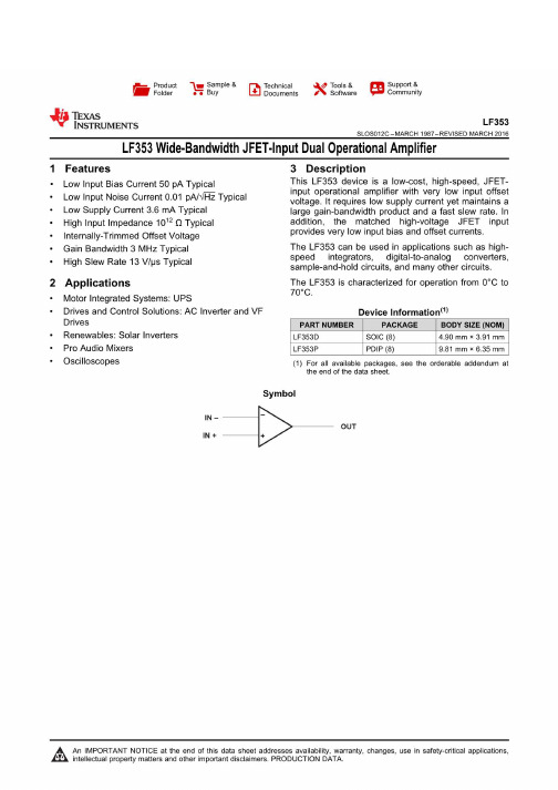
应用手册●电压跟随器图3 电压跟随器电路●增益为10的反相放大器图4 增益为10的反相放大器电路封装信息器件采用8引线D型封装和8引线T型封装。
D型封装外形尺寸按GB/T 7092-1993的规定,未注公差的尺寸按GB/T 1804-2000执行,外形尺寸如图5和表3所示。
T型封装外形尺寸按图6和表4的规定。
图5 D型(D08S2)陶瓷双列8线表3 D型(D08S2)封装外形尺寸图6 T型(T08A4)金属圆8线。
LF353中文资料_数据手册_参数
D低输入偏置电流…50 pA型低输入噪声电流0.01 pA/√Hz型低输入噪声电压…18 nV/√Hz型低供电电流…3.6 mA型高输入阻抗…1012年ΩTypD内部削减抵消电压增益带宽……3mhz类型,高转化率…13 V /µs TypdescriptionThis设备是一个低成本、高速、JFET-input运算放大器输入补偿电压很低。
它要求低的供电电流,但LF353保持了一个大的增益带宽产品和快速的转换速度。
此外,调制的高压JFET输入提供非常低的输入偏置和偏置电流。
LF353可用于高速积分器、数模转换器、采样保持电路和许多其他电路。
LF353的特点是在0°C到70°C之间运行。
(每个放大器的输出值+可用选项)包装可用胶带和卷绕。
将后缀R添加到设备类型(即。
LF353DR)。
绝对最大额定参数在操作自由空气的温度范围(除非另外说明)电源电压应用提示(续)由于将输入提高到共模范围内,再次将输入级和放大器置于正常工作模式。
超过单个输入的正共模极限不会改变输出的相位;然而,如果两者都超过了极限,放大器的输出将被迫处于高状态。
放大器的工作将与共模输入电压年龄等于正电源;然而,在这种情况下,增益带宽和旋转速率可能会降低。
当负共模电压荡到负电源的3v以内时,输入偏置伏特可能增加。
每个放大器由齐纳基准分别偏置,允许在±6V功率支持下正常电路运行。
LF353电源电压低于这些可能导致低增益带宽和摆频。
放大器将drivea2kΩ负载电阻±10 v在全温度范围0˚C + 70˚C。
然而,如果放大器被迫驱动更大的负载电流,则可能在负伏特翼上出现输入偏置电压的增加,并最终在正振荡和负振荡上达到有源电流的极限。
LF353应采取措施确保权力supplyfor集成电路不会成为逆转polarityor单位不是无意中安装在asocket向后无限通过resultingforward二极管集成电路中的电流冲击可能导致融合internalconductors和导致破坏单元。
实验十二集成运算放大器的测试解读
实验十二集成运算放大器的测试一、实验目的了解集成运算放大器的基本组成,掌握用集成运算放大器输入失调电压、输入失调电流等主要参数的测量方法。
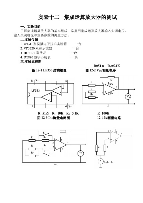
二.实验仪器1. WL-G型模拟电子技术实验箱一台2. VP5220双踪示波器一台3. HG2172毫伏表一台4. DT890数字万用表一块三.实验原理图R=51ΩR F=5.1K 图12-1 LF353结构框图图12-2 V OS测量电路R=51ΩR1=10K R F=5.1K R=100K图12-3 I OS测量电路图12-4 I B测量电路C=10uF R1=5.1K R 2=51Ω R F =100K C F =100uF 图12-5 A O 测量电路C=10uF R=1K R F =100K D=1N4148 图12-6 CMRR 测量电路 四、实验步骤与方法1.集成运算放大器 LF353为二运算放大器,该集成电路内含两个独立的运算放大器,内部结构、接线引脚如图12-1 所示。
2.测量输入失调电压V OS输入失调电压V OS 指在室温和标称电源电压下,为使集成运算放大器的输出电压为零,而在其输入端由恒压源提供的补偿电压值。
实验采用在输入信号为零的情况下,测量输出电压V O 的方法,间接的求出输入失调电压V OS ,按照图12-2连接电路,接入±15V 电源,用数字万用表测量输出电压V O 。
则输入失调电压V OS =。
3.测量输入失调电流I OS输入失调电流I OS 指在室温和标称电源电压下,当输入信号为零时,两输入端的基极偏置电流之差,按照图12-3连接电路,接入± 15V 电源,用数字万用表测量输出电压V O 。
当开关断开时为输出电压V O1,开关闭合时为V O2,则输入失调电流 I OS = × 。
R R +RV 2V1R 1R R +R4.测量输入偏置电流I B输入偏置电流I B 指在室温和标称电源电压下,当输入信号为零时,两输入端的基极电流的平均值,按照图12-4连接电路,接入±15V 电源,用数字万用表测量电流I,则基极偏置电流I B =I/2。
lf353工作原理
lf353工作原理
LF353是一款专用的宽带高速运算放大器。
该芯片由两个独立的、高性能的运算放大器组成,具有低噪声、高增益带宽和高输入电阻等特点。
它被广泛应用于精密量测和高保真音频放大器等领域。
LF353的工作原理基于差分对输入的放大器电路。
每个运算放大器由一个输入级、一个差动放大级和一个输出级组成。
输入级对输入信号进行阻抗扩展,并将信号传递给差动放大级。
差动放大器使用两个晶体管配对,将差分输入信号放大,并通过输出级将放大的信号输出。
在工作时,差分输入信号被分别连接到运放的非反相和反相输入端。
当输入信号的差异引起非线性失真时,差动放大器会通过增益控制来抵消这种失真。
差动放大器的增益与输出信号的相位差紧密相关,从而实现了对输入信号的线性放大。
LF353还具有高输入阻抗,这意味着它对输入信号的负载影响很小,从而使得输入信号的失真减小。
同时,该芯片的低噪声特性使其能够接收较小幅度的输入信号,并输出高保真度的放大信号。
总之,LF353的工作原理基于差分输入的放大器电路结构,通过差动放大器将输入信号放大,并通过输出级输出放大信号。
它的高增益带宽、低噪声和高输入阻抗等特性使其成为广泛应用于各种精密测量和音频放大器应用的理想选择。
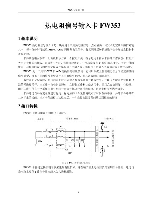
FW353使用手册
其它
工作温度
≥0℃,≤+50℃
工作湿度
≥5%,≤90%(不结露)
存储温度
≥-40℃,≤+70℃
存储湿度
≤95%(不结露)
工作大气压
≥62 kPa,≤108kPa
5 工程应用说明举例
FW353 热电阻输入卡支持两种信号类型:Pt100 和 Cu50 ,采用三线制测量方法。在工程应用 中,FW353 组态比较简单。首先根据信号选择类型组态,FW 353 有三种信号类型,Pt100、Cu50、 Pt100 小量程。Pt100 小量程应用在量程范围比较小,精度要求比较高的场所。
4 性能指标
表 4-1 FW353 性能指标
型号
FW353
电源
供电
5V 电源 24V 电源
(5±0.3)VDC,Imax<100mA (24±0.7)VDC,Imax<10mA
技术指标
通道数
8路
通道隔离方式
点点隔离
隔离电压
现场侧与系统侧 通道间
500VAC 50Hz 60s 60VAC 50Hz 60s
3.5 端子板选择
FW353 热电阻信号输入卡在使用时必须与对应的端子板配合使用。选配标准如下:
表 3-3 FW353 的端子板选配
描述 8 路热电阻 RTD 输入端子板 16 路热电阻 RTD 输入端子板
型号 TB353-R
TB353
使用范围 电阻信号 电阻信号
备注 可配置两冗余 FW353 卡 可配置两不冗余 FW353 卡
卡件通过自动标定系统进行标定,标定后的卡件采样精度可长时间保持不变。另外卡件还具有 二次标定的功能,当对卡件进行二次标定后,卡件在特定温度段能够达到很高的精度。
【学前教育】数字低电阻表

数字低电阻表嘿,科技迷们,今天咱们来聊聊一个超级酷炫又实用的工具——数字低电阻表! 你是否曾经为了测量微小电阻而头疼不已?是否渴望拥有一款能够精准到小数点后几位的神器?来来来,让我带你一探究竟!首先,咱们得明确一个核心观点:数字低电阻表,那可是电子工程师、物理实验员、电工维修大师们的得力助手! 它不仅能够帮助我们快速准确地测量出电路中的微小电阻值,还能在科研、教学、工业生产等多个领域大放异彩!想象一下,当你面对一个复杂的电路板,需要找到那个隐藏的“电阻小妖精”时,数字低电阻表就像是一双透视眼,让你瞬间锁定目标! 只需轻轻一按,屏幕上就能显示出精确到小数点后好几位的电阻值,是不是超级给力?而且啊,这款神器还超级智能! 它能够自动识别不同的电阻范围,自动选择合适的量程,让你无需手动调节,就能轻松搞定各种测量任务。
这简直就是为懒人量身定制的福利嘛!不过,说到这里,你有没有想过一个问题:为什么数字低电阻表能够如此精准呢? 其实啊,这都得益于它内部的高精度传感器和先进的数字信号处理技术。
这些高科技元素相互配合,就像是一群默契十足的舞伴,在舞台上演绎出一场场精彩的测量盛宴!当然啦,数字低电阻表也不是万能的。
在使用过程中,我们还是需要注意一些细节问题的。
比如,要确保测量引线的接触良好,避免因为接触不良而导致的测量误差;还要根据被测电阻的大小选择合适的量程,避免因为量程过大或过小而导致的测量不准确。
说到这里,我想到了一个有趣的话题:你觉得数字低电阻表在未来会有哪些创新和发展呢? 是会更加智能化、自动化,还是会在精度和稳定性上有更大的突破?快来评论区告诉我你的看法吧!最后啊,我要提醒大家一句:虽然数字低电阻表是个好东西,但也不能盲目追求高精度哦! 在实际应用中,我们要根据具体需求来选择合适的测量工具,这样才能真正做到事半功倍!好啦,今天的分享就到这里啦!如果你对数字低电阻表还有其他疑问或者想了解更多相关信息,记得点赞收藏加关注哦! 让我们一起在科技的海洋中畅游吧!结尾争议话题:有人说,数字低电阻表的出现彻底颠覆了传统电阻测量的方式,让测量变得更加简单快捷;但也有人觉得,传统电阻表在某些方面仍然有着不可替代的作用。
LF353运放构成振荡电路
LF353运放构成振荡电路振荡电路如图1所示.由带通滤波器和反相放大器组成。
由R2、C2、R1、C1组成的带通滤波器构成放大器的正反馈电路。
当设定R1=R2=R.C1=C2=C时.在频率为fo时带通滤波器的相位为零。
因此.当把运算放大器的反馈电阻R3和R4设定为R3=2R4时.同相放大器的增益为3倍,在fo处的环路增益正好为1倍,电路产生振荡,并正好能维持振荡。
振荡频率可用fo=1/2πRC进行计算.方法如下:1.给定振荡频率fo和电阻R的值,计算电容器C的值。
例如设fo=1000Hz,R=10kΩ,则可以求得C=0.0159μF。
2.给定振荡频率fo和电容C的值,计算电阻R的值。
由于0.0159μF不是电容器的标称值.必须用几个电容器经串并联组合后才能实现,在制作电路时不但成本高,操作起来也很麻烦。
因此可以先确定电容量,再求电阻阻值。
例如此时将电容量设定为C=0.0159μF,即R=1/2πfoC=10.6kΩ。
对于该振荡电路来说即使环路增益只比1倍稍稍小一点点,电路也不会振荡。
所以在设计实际的电路时为了能确保振荡.将R3和R4设定为R3=2.2 R4的关系。
此时可以确保振荡.但又带来振荡会随时间不断增加,最后导致波形顶部被限幅的问题。
为此需在反馈电路中接入稳压二极管对振幅的增加进行限制。
图2是输出电压为2Vrms,振荡频率为1kHz的振荡电路的例子。
电路的输出阻抗为600Ω。
负反馈量减小放大器的环路增益。
振荡电路的谐波失真率约为0.5%,开机后振幅会不断增大,约需5ms才会稳定下来。
这种振荡电路存在振幅会因R1和R2的误差或者C1和C2的误差而变化,这是这种振荡电路的不足之处。
例如在图3的电路中若R=2.2kΩ,将C2从0.015μF变为0.016μF,振荡电路的振幅会以7Vrms变成9.3Vms.这种振荡电路可振荡的频率范围很宽.可以从数赫兹到数百赫兹。
3.3v 下拉电阻电路
3.3v 下拉电阻电路
在3.3V的下拉电阻电路中,电阻的一端通常连接到GND(即0V),另一端连接到需要被下拉到低电平的逻辑电平接入引脚,如单片机的某个引脚。
这种连接方式可以确保当引脚未被其他电路驱动为高电平时,通过下拉电阻的作用,引脚电平会被拉低至低电平(0V),从而确保电路的稳定性和可靠性。
在实际应用中,下拉电阻的阻值选择需要根据具体电路的需求和引脚的驱动能力来确定。
阻值过大可能会导致下拉效果不佳,而阻值过小则可能会增加功耗和电路的复杂性。
此外,需要注意的是,在设计下拉电阻电路时,还需要考虑电路中的其他元件和因素,如电源的稳定性、噪声干扰等。
因此,在实际应用中,需要根据具体情况进行综合考虑和设计。
lf353工作原理
lf353工作原理
LF353是一种高速低功耗双运放,其工作原理如下:
1. 电流放大器:LF353的输入阻抗非常高,通常在10^12Ω的范围内。
它将输入电流放大为相应的输出电压。
输入电流一般很小,可忽略不计。
2. 差动放大器:LF353有两个输入引脚,一个是非反馈输入引脚(即正输入引脚)(+),另一个是反馈输入引脚(即负输入引脚)(-)。
它们之间的电压差称为差动输入电压。
差动放大器根据差动输入电压放大和输出一个信号。
3. 反相放大器:LF353可以通过连接一个适当的电阻和电容将差动输入引脚连接到输出引脚,从而形成一个反相放大器。
当差动输入电压发生变化时,经过放大后的信号会在输出引脚上生成一个反相的输出电压。
4. 非反相放大器:通过改变差动输入引脚和输出引脚之间的连接方式,可以将LF353设置为非反相放大器。
当差动输入电压变化时,经过放大后的信号会在输出引脚上生成一个与输入信号同相的输出电压。
总之,LF353通过差动放大器的原理将输入信号放大并进行反相或非反相处理,最终输出一个放大后的信号。
LF353MX,LF353MNOPB,LF353NNOPB, 规格书,Datasheet 资料
LF353LF353 Wide Bandwidth Dual JFET Input Operational AmplifierLiterature Number: SNOSBH3D 芯天下--/LF353Wide Bandwidth Dual JFET Input Operational AmplifierGeneral DescriptionThese devices are low cost,high speed,dual JFET input operational amplifiers with an internally trimmed input offset voltage (BI-FET II ™technology).They require low supply current yet maintain a large gain bandwidth product and fast slew rate.In addition,well matched high voltage JFET input devices provide very low input bias and offset currents.The LF353is pin compatible with the standard LM1558allowing designers to immediately upgrade the overall performance of existing LM1558and LM358designs.These amplifiers may be used in applications such as high speed integrators,fast D/A converters,sample and hold circuits and many other circuits requiring low input offset voltage,low input bias current,high input impedance,high slew rate and wide bandwidth.The devices also exhibit low noise and offset voltage drift.Featuresn Internally trimmed offset voltage:10mV n Low input bias current:50pA n Low input noise voltage:25nV/√Hz n Low input noise current:0.01pA/√Hzn Wide gain bandwidth:4MHz n High slew rate:13V/µs n Low supply current: 3.6mA n High input impedance:1012Ωn Low total harmonic distortion :≤0.02%n Low 1/f noise corner:50Hz nFast settling time to 0.01%:2µsTypical Connection 00564914Simplified Schematic1/2Dual00564916Connection DiagramDual-In-Line Package00564917Top ViewOrder Number LF353M,LF353MX or LF353N See NS Package Number M08A or N08EBI-FET II ™is a trademark of National Semiconductor Corporation.December 2003LF353Wide Bandwidth Dual JFET Input Operational Amplifier©2003National Semiconductor Corporation Absolute Maximum Ratings (Note 1)If Military/Aerospace specified devices are required,please contact the National Semiconductor Sales Office/Distributors for availability and specifications.Supply Voltage ±18VPower Dissipation(Note 2)Operating Temperature Range 0˚C to +70˚CT j (MAX)150˚CDifferential Input Voltage ±30V Input Voltage Range (Note 3)±15VOutput Short Circuit Duration Continuous Storage Temperature Range −65˚C to +150˚CLead Temp.(Soldering,10sec.)260˚CSoldering Information Dual-In-Line Package Soldering (10sec.)260˚CSmall Outline Package Vapor Phase (60sec.)215˚C Infrared (15sec.)220˚CSee AN-450“Surface Mounting Methods and Their Effect on Product Reliability”for other methods of soldering surface mount devices.ESD Tolerance (Note 8)1000V θJA M PackageTBDNote 1:Absolute Maximum Ratings indicate limits beyond which damage to the device may occur.Operating ratings indicate conditions for which the device is functional,but do not guarantee specific performance limits.Elec-trical Characteristics state DC and AC electrical specifications under particu-lar test conditions which guarantee specific performance limits.This assumes that the device is within the Operating Ratings.Specifications are not guar-anteed for parameters where no limit is given,however,the typical value is a good indication of device performance.DC Electrical Characteristics(Note 5)Symbol ParameterConditionsLF353Units MInTyp Max V OS Input Offset VoltageR S =10k Ω,T A =25˚C 510mV Over Temperature 13mV ∆V OS /∆T Average TC of Input Offset Voltage R S =10k Ω10µV/˚C I OS Input Offset Current T j =25˚C,(Notes 5,6)25100pA T j ≤70˚C4nA I B Input Bias Current T j =25˚C,(Notes 5,6)50200pA T j ≤70˚C 8nA R IN Input ResistanceT j =25˚C1012ΩA VOLLarge Signal Voltage GainV S =±15V,T A =25˚C 25100V/mVV O =±10V,R L =2k ΩOver Temperature15V/mVV O Output Voltage Swing V S =±15V,R L =10k Ω±12±13.5V V CM Input Common-Mode Voltage V S =±15V±11+15V Range−12V CMRR Common-Mode Rejection Ratio R S ≤10k Ω70100dB PSRR Supply Voltage Rejection Ratio (Note 7)70100dB I SSupply Current3.66.5mAAC Electrical Characteristics(Note 5)SymbolParameterConditionsLF353UnitsMinTyp MaxAmplifier to Amplifier CouplingT A =25˚C,f=1Hz−20kHz −120dB (Input Referred)SR Slew RateV S =±15V,T A =25˚C 8.013V/µs GBW Gain Bandwidth Product V S =±15V,T A =25˚C 2.74MHze n Equivalent Input Noise Voltage T A =25˚C,R S =100Ω,16f=1000Hzi nEquivalent Input Noise CurrentT j =25˚C,f=1000Hz0.01L F 353 2AC Electrical Characteristics(Continued)(Note5)Symbol Parameter Conditions LF353UnitsMin Typ MaxTHD Total Harmonic Distortion A V=+10,RL=10k,V O=20Vp−p,BW=20Hz-20kHz<0.02%Note2:For operating at elevated temperatures,the device must be derated based on a thermal resistance of115˚C/W typ junction to ambient for the N package, and158˚C/W typ junction to ambient for the H package.Note3:Unless otherwise specified the absolute maximum negative input voltage is equal to the negative power supply voltage.Note4:The power dissipation limit,however,cannot be exceeded.Note5:These specifications apply for V S=±15V and0˚C≤T A≤+70˚C.V OS,I B and I OS are measured at V CM=0.Note6:The input bias currents are junction leakage currents which approximately double for every10˚C increase in the junction temperature,T j.Due to the limited production test time,the input bias currents measured are correlated to junction temperature.In normal operation the junction temperature rises above the ambient temperature as a result of internal power dissipation,P D.T j=T A+θjA P D whereθjA is the thermal resistance from junction to e of a heat sink is recommended if input bias current is to be kept to a minimum.Note7:Supply voltage rejection ratio is measured for both supply magnitudes increasing or decreasing simultaneously in accordance with common practice.V S =±6V to±15V.Note8:Human body model,1.5kΩin series with100pF.Typical Performance CharacteristicsInput Bias Current Input Bias Current0056491800564919Supply Current Positive Common-Mode Input Voltage Limit0056492000564921LF3533Typical Performance Characteristics(Continued)Negative Common-Mode Input Voltage LimitPositive Current Limit0056492200564923Negative Current Limit Voltage Swing0056492400564925Output Voltage Swing Gain Bandwidth0056492600564927L F 353 4Typical Performance Characteristics(Continued)Bode PlotSlew Rate0056492800564929Distortion vs.Frequency Undistorted Output Voltage Swing0056493000564931Open Loop Frequency Response Common-Mode Rejection Ratio0056493200564933LF3535Typical Performance Characteristics(Continued)Power Supply Rejection RatioEquivalent Input Noise Voltage0056493400564935Open Loop Voltage Gain (V/V)Output Impedance0056493600564937Inverter Settling Time00564938L F 353 6Pulse ResponseSmall Signaling Inverting00564904Large Signal Inverting00564906Small Signal Non-Inverting00564905Large Signal Non-Inverting00564907Current Limit(R L=100Ω)00564908Application HintsThese devices are op amps with an internally trimmed inputoffset voltage and JFET input devices(BI-FET II).TheseJFETs have large reverse breakdown voltages from gate tosource and drain eliminating the need for clamps across theinputs.Therefore,large differential input voltages can easilybe accommodated without a large increase in input current.The maximum differential input voltage is independent of thesupply voltages.However,neither of the input voltagesshould be allowed to exceed the negative supply as this willcause large currents to flow which can result in a destroyedunit.Exceeding the negative common-mode limit on either inputwill force the output to a high state,potentially causing areversal of phase to the output.Exceeding the negativecommon-mode limit on both inputs will force the amplifieroutput to a high state.In neither case does a latch occurLF3537Application Hints(Continued)since raising the input back within the common-mode range again puts the input stage and thus the amplifier in a normal operating mode.Exceeding the positive common-mode limit on a single input will not change the phase of the output;however,if both inputs exceed the limit,the output of the amplifier will be forced to a high state.The amplifiers will operate with a common-mode input volt-age equal to the positive supply;however,the gain band-width and slew rate may be decreased in this condition.When the negative common-mode voltage swings to within 3V of the negative supply,an increase in input offset voltage may occur.Each amplifier is individually biased by a zener reference which allows normal circuit operation on ±6V power sup-plies.Supply voltages less than these may result in lower gain bandwidth and slew rate.The amplifiers will drive a 2k Ωload resistance to ±10V over the full temperature range of 0˚C to +70˚C.If the amplifier is forced to drive heavier load currents,however,an increase in input offset voltage may occur on the negative voltage swing and finally reach an active current limit on both posi-tive and negative swings.Precautions should be taken to ensure that the power supply for the integrated circuit never becomes reversed in polarityor that the unit is not inadvertently installed backwards in a socket as an unlimited current surge through the resulting forward diode within the IC could cause fusing of the internal conductors and result in a destroyed unit.As with most amplifiers,care should be taken with lead dress,component placement and supply decoupling in order to ensure stability.For example,resistors from the output to an input should be placed with the body close to the input to minimize “pick-up”and maximize the frequency of the feed-back pole by minimizing the capacitance from the input to ground.A feedback pole is created when the feedback around any amplifier is resistive.The parallel resistance and capacitance from the input of the device (usually the inverting input)to AC ground set the frequency of the pole.In many instances the frequency of this pole is much greater than the expected 3dB frequency of the closed loop gain and consequently there is negligible effect on stability margin.However,if the feed-back pole is less than approximately 6times the expected 3dB frequency a lead capacitor should be placed from the output to the input of the op amp.The value of the added capacitor should be such that the RC time constant of this capacitor and the resistance it parallels is greater than or equal to the original feedback pole time constant.Detailed Schematic00564909L F 353 8Typical ApplicationsThree-Band Active Tone Control0056493900564940Note 1:All controls flat.Note 2:Bass and treble boost,mid flat.Note 3:Bass and treble cut,mid flat.Note 4:Mid boost,bass and treble flat.Note 5:Mid cut,bass and treble flat.•All potentiometers are linear taper•Use the LF347Quad for stereo applicationsLF3539Typical Applications(Continued)Improved CMRR Instrumentation Amplifier00564941Fourth Order Low Pass Butterworth Filter00564942L F 353 10Typical Applications(Continued)Fourth Order High Pass Butterworth Filter00564943LF35311Typical Applications(Continued)Ohms to Volts Converter00564944L F 353 12Physical Dimensionsinches (millimeters)unless otherwise notedOrder Number LF353M or LF353MXNS Package Number M08AMolded Dual-In-Line PackageOrder Number LF353N NS Package N08ELF35313NotesLIFE SUPPORT POLICYNATIONAL’S PRODUCTS ARE NOT AUTHORIZED FOR USE AS CRITICAL COMPONENTS IN LIFE SUPPORT DEVICES OR SYSTEMS WITHOUT THE EXPRESS WRITTEN APPROVAL OF THE PRESIDENT AND GENERAL COUNSEL OF NATIONAL SEMICONDUCTOR CORPORATION.As used herein:1.Life support devices or systems are devices or systems which,(a)are intended for surgical implant into the body,or (b)support or sustain life,and whose failure to perform when properly used in accordance with instructions for use provided in the labeling,can be reasonably expected to result in a significant injury to the user. 2.A critical component is any component of a life support device or system whose failure to perform can be reasonably expected to cause the failure of the life support device or system,or to affect its safety or effectiveness.BANNED SUBSTANCE COMPLIANCENational Semiconductor certifies that the products and packing materials meet the provisions of the Customer Products Stewardship Specification (CSP-9-111C2)and the Banned Substances and Materials of Interest Specification (CSP-9-111S2)and contain no ‘‘Banned Substances’’as defined in CSP-9-111S2.National Semiconductor Americas Customer Support CenterEmail:new.feedback@ Tel:1-800-272-9959National SemiconductorEurope Customer Support CenterFax:+49(0)180-5308586Email:europe.support@Deutsch Tel:+49(0)6995086208English Tel:+44(0)8702402171Français Tel:+33(0)141918790National Semiconductor Asia Pacific Customer Support CenterEmail:ap.support@National SemiconductorJapan Customer Support Center Fax:81-3-5639-7507Email:jpn.feedback@ Tel:81-3-5639-7560L F 353W i d e B a n d w i d t h D u a l J F E T I n p u t O p e r a t i o n a l A m p l i f i e rNational does not assume any responsibility for use of any circuitry described,no circuit patent licenses are implied and National reserves the right at any time without notice to change said circuitry and specifications.IMPORTANT NOTICETexas Instruments Incorporated and its subsidiaries(TI)reserve the right to make corrections,modifications,enhancements,improvements, and other changes to its products and services at any time and to discontinue any product or service without notice.Customers should obtain the latest relevant information before placing orders and should verify that such information is current and complete.All products are sold subject to TI’s terms and conditions of sale supplied at the time of order acknowledgment.TI warrants performance of its hardware products to the specifications applicable at the time of sale in accordance with TI’s standard warranty.Testing and other quality control techniques are used to the extent TI deems necessary to support this warranty.Except where mandated by government requirements,testing of all parameters of each product is not necessarily performed.TI assumes no liability for applications assistance or customer product design.Customers are responsible for their products and applications using TI components.To minimize the risks associated with customer products and applications,customers should provide adequate design and operating safeguards.TI does not warrant or represent that any license,either express or implied,is granted under any TI patent right,copyright,mask work right, or other TI intellectual property right relating to any combination,machine,or process in which TI products or services are rmation published by TI regarding third-party products or services does not constitute a license from TI to use such products or services or a warranty or endorsement e of such information may require a license from a third party under the patents or other intellectual property of the third party,or a license from TI under the patents or other intellectual property of TI.Reproduction of TI information in TI data books or data sheets is permissible only if reproduction is without alteration and is accompanied by all associated warranties,conditions,limitations,and notices.Reproduction of this information with alteration is an unfair and deceptive business practice.TI is not responsible or liable for such altered rmation of third parties may be subject to additional restrictions.Resale of TI products or services with statements different from or beyond the parameters stated by TI for that product or service voids all express and any implied warranties for the associated TI product or service and is an unfair and deceptive business practice.TI is not responsible or liable for any such statements.TI products are not authorized for use in safety-critical applications(such as life support)where a failure of the TI product would reasonably be expected to cause severe personal injury or death,unless officers of the parties have executed an agreement specifically governing such use.Buyers represent that they have all necessary expertise in the safety and regulatory ramifications of their applications,and acknowledge and agree that they are solely responsible for all legal,regulatory and safety-related requirements concerning their products and any use of TI products in such safety-critical applications,notwithstanding any applications-related information or support that may be provided by TI.Further,Buyers must fully indemnify TI and its representatives against any damages arising out of the use of TI products in such safety-critical applications.TI products are neither designed nor intended for use in military/aerospace applications or environments unless the TI products are specifically designated by TI as military-grade or"enhanced plastic."Only products designated by TI as military-grade meet military specifications.Buyers acknowledge and agree that any such use of TI products which TI has not designated as military-grade is solely at the Buyer's risk,and that they are solely responsible for compliance with all legal and regulatory requirements in connection with such use. TI products are neither designed nor intended for use in automotive applications or environments unless the specific TI products are designated by TI as compliant with ISO/TS16949requirements.Buyers acknowledge and agree that,if they use any non-designated products in automotive applications,TI will not be responsible for any failure to meet such requirements.Following are URLs where you can obtain information on other Texas Instruments products and application solutions:Products ApplicationsAudio /audio Communications and Telecom /communicationsAmplifiers Computers and Peripherals /computersData Converters Consumer Electronics /consumer-appsDLP®Products Energy and Lighting /energyDSP Industrial /industrialClocks and Timers /clocks Medical /medicalInterface Security /securityLogic Space,Avionics and Defense /space-avionics-defense Power Mgmt Transportation and Automotive /automotiveMicrocontrollers Video and Imaging /videoRFID OMAP Mobile Processors /omapWireless Connectivity /wirelessconnectivityTI E2E Community Home Page Mailing Address:Texas Instruments,Post Office Box655303,Dallas,Texas75265Copyright©2011,Texas Instruments Incorporated。