开关电源设计手册 SMPS design
第六章内容
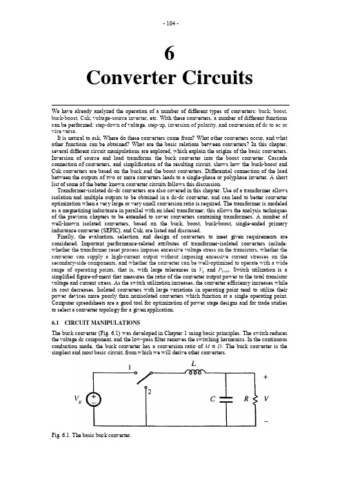
6Converter CircuitsWe have already analyzed the operation of a number of different types of converters: buck, boost,buck-boost, Cuk, voltage-source inverter, etc. With these converters, a number of different functionscan be performed: step-down of voltage, step-up, inversion of polarity, and conversion of dc to ac orvice versa.It is natural to ask, Where do these converters come from? What other converters occur, and whatother functions can be obtained? What are the basic relations between converters? In this chapter,several different circuit manipulations are explored, which explain the origins of the basic converters.Inversion of source and load transforms the buck converter into the boost converter. Cascadeconnection of converters, and simplification of the resulting circuit, shows how the buck-boost andCuk converters are based on the buck and the boost converters. Differential connection of the loadbetween the outputs of two or more converters leads to a single-phase or polyphase inverter. A shortlist of some of the better known converter circuits follows this discussion.Transformer-isolated dc-dc converters are also covered in this chapter. Use of a transformer allowsisolation and multiple outputs to be obtained in a dc-dc converter, and can lead to better converter optimization when a very large or very small conversion ratio is required. The transformer is modeledas a magnetizing inductance in parallel with an ideal transformer; this allows the analysis techniquesof the previous chapters to be extended to cover converters containing transformers. A number ofwell-known isolated converters, based on the buck, boost, buck-boost, single-ended primaryinductance converter (SEPIC), and Cuk, are listed and discussed.Finally, the evaluation, selection, and design of converters to meet given requirements areconsidered. Important performance-related attributes of transformer-isolated converters include:whether the transformer reset process imposes excessive voltage stress on the transistors, w hether theconverter can supply a high-current output without imposing excessive current stresses on thesecondary-side components, and whether the converter can be well-optimized to operate with a widerange of operating points, that is, with large tolerances in V g and P load. Switch utilization is asimplified figure-of-merit that measures the ratio of the converter output power to the total transistorvoltage and current stress. As the switch utilization increases, the converter efficiency increases whileits cost decreases. Isolated converters with large variations in operating point tend to utilize theirpower devices more poorly than nonisolated converters which function at a single operating point.Computer spreadsheets are a good tool for optimization of power stage designs and for trade studiesto select a converter topology for a given application.6.1 CIRCUIT MANIPULATIONSThe buck converter (Fig. 6.1) was developed in Chapter 1 using basic principles. The switch reducesthe voltage dc component, and the low-pass filter removes the switching harmonics. In the continuousconduction mode, the buck converter has a conversion ratio of M =D. The buck converter is thesimplest and most basic circuit, from which we will derive other converters.Fig. 6.1. The basic buck converter.6.1.1 Inversion of Source and LoadLet us consider first what happens when we interchange the power input and power output ports of a converter. In the buck converter of Fig. 6.2(a), voltage V 1 is applied at port 1, and voltage V 2 appears at port 2. We know thatV 2 = DV 1 (6.1)This equation can be derived using the principle of inductor volt-second balance, with the assumption that the converter operates in the continuous conduction mode. Provided that the switch is realized such that this assumption holds, then Eq. (6.1) is true regardless of the direction of power flow.Fig. 6.2. Inversion of source and load transforms a buck converter into a boost converter: (a) buck converter, (b) inversion of source and load, (c) realization of switch.So let us interchange the power source and load, as in Fig. 6.2(b). The load, bypassed by the capacitor, is connected to converter port 1, while the power source is connected to converter port 2. Power now flows in the opposite direction through the converter. Equation (6.1) must still hold; by solving for the load voltage V 1, one obtains211V DV =(6.2) So the load voltage is greater than the source voltage. Figure 6.2(b) is a boost converter, drawn backwards. Equation (6.2) nearly coincides with the familiar boost converter result, M (D )= 1/D ', except that D ' is replaced by D .Since power flows in the opposite direction, the standard buck converter unidirectional switch realization cannot be used with the circuit of Fig. 6.2(b). By following the discussion of Chapter 4, one finds that the switch can be realized by connecting a transistor between the inductor and ground, and a diode from the inductor to the load, as shown in Fig. 6.2(c). In consequence, the transistor duty cycle D becomes the fraction of time which the single-pole double-throw (SPDT) switch of Fig. 6.2(b)spends in position 2, rather than in position 1. So we should interchange D with its complement D ' in Eq. (6.2), and the conversion ratio of the converter of Fig. 6.2(c) is21'1V D V =(6.3) Thus, the boost converter can be viewed as a buck converter having the source and load connections exchanged, and in which the switch is realized in a manner that allows reversal of the direction of power flow.Fig. 6.3. Cascade connection of converters.6.1.2 Cascade Connection of Converters Converters can also be connected in cascade, as illustrated in Fig. 6.3 [1,2]. Converter 1 has conversion ratio M 1(D ), such that its output voltage V 1 isg V D M V )(11= (6.4)This voltage is applied to the input of the second converter. Let us assume that converter 2 is driven with the same duty cycle D applied to converter 1. If converter 2 has conversion ratio M 2(D ), then the output voltage V is12)(V D M V = (6.5) Substitution of Eq. (6.4) into Eq. (6.5) yields)()()(21D M D M D M V V g== (6.6) Hence, the conversion ratio M (D ) of the composite converter is the product of the individual conversion ratios M 1(D ) and M 2(D ).Fig. 6.4. Cascade connection of buck converter and boost converter.Let us consider the case where converter 1 is a buck converter, and converter 2 is a boost converter. The resulting circuit is illustrated in Fig. 6.4. The buck converter has conversion ratioD V V g=1 (6.7) The boost converter has conversion ratioDV −11So the composite conversion ratio isDD V V g −=1 (6.9) The composite converter has a noninverting buck-boost conversion ratio. The voltage is reduced whenD < 0.5, and increased when D > 0.5.Fig. 6.5. Simplification of the cascaded buck and boost converter circuit of Fig. 6.4: (a) removal of capacitor C 1, (b) combining of inductors L 1 and L 2.The circuit of Fig. 6.4 can be simplified considerably. Note that inductors L 1 and L 2, along with capacitor C 1, form a three-pole low-pass filter. The conversion ratio does not depend on the number of poles present in the low-pass filter, and so the same steady-state output voltage should be obtained when a simpler low-pass filter is used. In Fig. 6.5(a), capacitor C 1 is removed. Inductors L 1 and L 2 are now in series, and can be combined into a single inductor as shown in Fig. 6.5(b). This converter, the noninverting buck-boost converter, continues to exhibit the conversion ratio given in Eq. (6.9).Fig. 6.6. Connections of the circuit of Fig. 6.5(b): (a) while the switches are in position 1, (b) while the switches are in position 2.The switches of the converter of Fig. 6.5(b) can also be simplified, leading to a negative output voltage. When the switches are in position 1, the converter reduces to Fig. 6.6(a). The inductor is connected to the input source V g and energy is transferred from the source to the inductor. When the switches are in position 2, the converter reduces to Fig. 6.6(b). The inductor is then connected to the load, and energy is transferred from the inductor to the load. To obtain a negative output, we can simply reverse the polarity of the inductor during one of the subintervals (say, while the switches are in position 2). The individual circuits of Fig. 6.7 are then obtained, and the conversion ratio becomesDV g −1Note that one side of the inductor is now always connected to ground, while the other side is switched between the input source and the load. Hence only one SPDT switch is needed, and the converter circuit of Fig. 6.8 is obtained. Figure 6.8 is recognized as the conventional buck-boost converter.Fig. 6.7. Reversal of the output voltage polarity, by reversing the inductor connections while the switches are in position 2: (a) connections with the switches in position 1, (b) connections with the switches in position 2.Fig. 6.8. Converter circuit obtained from the subcircuits of Fig. 6.7.Thus, the buck-boost converter can be viewed as a cascade connection of buck and boost converters. The properties of the buck-boost converter are consistent with this viewpoint. Indeed, the equivalent circuit model of the buck-boost converter contains a 1:D (buck) dc transformer, followed by a D ':1 (boost) dc transformer. The buck-boost converter inherits the pulsating input current of the buck converter, and the pulsating output current of the boost converter.Other converters can be derived by cascade connections. The Cuk converter (Fig. 2.20) was originally derived [1,2] by cascading a boost converter (converter 1), followed by a buck (converter 2).A negative output voltage is obtained by reversing the polarity of the internal capacitor connection during one of the subintervals; as in the buck-boost converter, this operation has the additional benefit of reducing the number of switches. The equivalent circuit model of the Cuk converter contains a D ':1 (boost) ideal dc transformer, followed by a 1:D (buck) ideal dc transformer. The Cuk converter inherits the nonpulsating input current property of the boost converter, and the nonpulsating output current property of the buck converter.6.1.3 Rotation of Three-Terminal CellThe buck, boost, and buck-boost converters each contain an inductor that is connected to a SPDT switch. As illustrated in Fig. 6.9(a), the inductor-switch network can be viewed as a basic cell having the three terminals labeled a , b , and c . It was first pointed out in [1,2], and later in [3], that there are three distinct ways to connect this cell between the source and load. The connections a-A b-B c-C lead to the buck converter. The connections a-C b-A c-B amount to inversion of the source and load, and lead to the boost converter. The connections a-A b-C c-B lead to the buck-boost converter. So the buck, boost, and buck-boost converters could be viewed as being based on the same inductor-switch cell, with different source and load connections.Fig. 6.9. Rotation of three-terminal switch cells: (a) switch/inductor cell, (b) switch/capacitor cell.A dual three-terminal network, consisting of a capacitor-switch cell, is illustrated in Fig. 6.9(b). Filter inductors are connected in series with the source and load, such that the converter input and output currents are nonpulsating. There are again three possible ways to connect this cell between the source and load. The connections a-A b-B c-C lead to a buck converter with L-C input low-pass filter. The connections a-B b-A c-C coincide with inversion of source and load, and lead to a boost converter with an added output L-C filter section. The connections a-A b-C c-B lead to the Cuk converter. Rotation of more complicated three-terminal cells is explored in [4].6.1.4 Differential Connection of the LoadIn inverter applications, where an ac output is required, a converter is needed that is capable of producing an output voltage of either polarity. By variation of the duty cycle in the correct manner, a sinusoidal output voltage having no dc bias can then be obtained. Of the converters studied so far in this chapter, the buck and the boost can produce only a positive unipolar output voltage, while the buck-boost and Cuk converter produce only a negative unipolar output voltage. How can we derive converters that can produce bipolar output voltages?Fig. 6.10. Obtaining a bipolar output by differential connection of load.A well-known technique for obtaining a bipolar output is the differential connection of the load across the outputs of two known converters, as illustrated in Fig. 6.10. If converter 1 produces voltagedc source V 1, and converter 2 produces voltage V 2, then the load voltage V is given by21V V V −= (6.11)Although V 1 and V 2 may both individually be positive, the load voltage V can be either positive or negative. Typically, if converter 1 is driven with duty cycle D , then converter 2 is driven with its complement, D ', so that when V 1 increases, V 2 decreases, and vice versa.Several well-known inverter circuits can be derived using the differential connection. Let’s realize converters 1 and 2 of Fig. 6.10 using buck converters. Figure 6.11(a) is obtained. Converter 1 is driven with duty cycle D , while converter 2 is driven with duty cycle D '. So when the SPDT switch of converter 1 is in the upper position, then the SPDT switch of converter 2 is in the lower position, and vice versa. Converter 1 then produces output voltage V 1 = DV g , while converter 2 produces output voltage V 2 = D'V g . The differential load voltage isg g V D DV V '−= (6.12)Simplification leads tog V D V )12(−= (6.13)This equation is plotted in Fig. 6.12. It can be seen the output voltage is positive for D > 0.5, and negative for D < 0.5. If the duty cycle is varied sinusoidally about a quiescent operating point of 0.5, then the output voltage will be sinusoidal, with no dc bias.The circuit of Fig. 6.11 (a) can be simplified. It is usually desired to bypass the load directly with a capacitor, as in Fig. 6.11(b). The two inductors are now effectively in series, and can be combined into a single inductor as in Fig. 6.11(c). Figure 6.11(d) is identical to Fig. 6.11(c), but is redrawn for clarity. This circuit is commonly called the H-bridge , or bridge inverter circuit. Its use is widespread in servo amplifiers and single-phase inverters. Its properties are similar to those of the buck converter, from which it is derived.Fig. 6.11. Derivation of bridge inverter (H-bridge): (a) differential connection of load across outputs of buck converters, (b) bypassing load by capacitor, (c) combining series inductors, (d) circuit (c) redrawn in its usual form.Fig. 6.12. Conversion ratio of the H-bridge inverter circuit.Fig. 6.13. Generation of dc-3Фac inverter by differential connection of 3Ф load.Polyphase inverter circuits can be derived in a similar manner. A three-phase load can be connected differentially across the outputs of three dc-dc converters, as illustrated in Fig. 6.13. If the three-phase load is balanced, then the neutral voltage V n will be equal to the average of the three converter output voltages:)(21321V V V V n ++= (6.14) If the converter output voltages V 1, V 2, and V 3 contain the same dc bias, then this dc bias will also appear at the neutral point V n . The phase voltages V an , V bn and V cn are given by ncn n bn nan V V V V V V V V V −=−=−=321 (6.15)It can be seen that the dc biases cancel out, and do not appear in V an , V bn , and V cn .Let us realize converters 1, 2, and 3 of Fig. 6.13 using buck converters. Figure 6.14(a) is then obtained. The circuit is redrawn in Fig. 6.l4(b) for clarity. This converter is known by several names, including the voltage-source inverter and the buck-derived three-phase bridge .Inverter circuits based on dc-dc converters other than the buck converter can be derived in a similar manner. Figure 6.14(c) contains a three-phase current-fed bridge converter having a boost-type voltage conversion ratio. Since most inverter applications require the capability to reduce the voltage magnitude, a dc-dc buck converter is usually casacded at the current-fed bridge dc input port. Several other examples of three-phase inverters are given in [5-7], in which the converters are capable of both increasing and decreasing the voltage magnitude.Fig. 6.14. Derivation of dc-3Фac inverters: (a) differential connection of 3Ф load across outputs of buck converters; (b) simplification of low-pass filters to obtain the dc-3Фac voltage-source inverter; (c) the dc-3Фac current-source inverter.Fig. 6.14. Continued.6.2 A SHORT LIST OF CONVERTERSAn infinite number of converters are possible, and hence it is not feasible to list them all here. A short list is given here.Let’s consider first the class of single-input single-output converters, containing a single inductor. There are a limited number of ways in which the inductor can be connected between the source and load. If we assume that the switching period is divided into two subintervals, then the inductor should be connected to the source and load in one manner during the first subinterval, and in a different manner during the second subinterval. One can examine all of the possible combinations, to derive the complete set of converters in this class [8-10]. By elimination of redundant and degenerate circuits, one finds that there are eight converters, listed in Fig. 6.15. How the converters are counted can actually be a matter of semantics and personal preference; for example, many people in the field would not consider the noninverting buck-boost converter as distinct from the inverting buck-boost. Nonetheless, it can be said that a converter is defined by the connections between its reactive elements, switches, source, and load; by how the switches are realized; and by the numerical range of reactive element values.Fig. 6.15. Eight members of the basic class of single-input single-output converters containing a single inductor.Fig. 6.15. Continued.The first four converters of Fig. 6.15, the buck, boost, buck-boost, and the noninverting buck-boost, have been previously discussed. These converters produce a unipolar dc output voltage.Converters 5 and 6 are capable of producing a bipolar output voltage. Converter 5, the H-bridge, has previously been discussed. Converter 6 is a nonisolated version of a push-pull current-fed converter [11-15]. This converter can also produce a bipolar output voltage; however, its conversion ratio M(D) is a nonlinear function of duty cycle. The number of switch elements can be reduced by using a two-winding inductor as shown. The function of the inductor is similar to that of the flyback converter, discussed in the next section. When switch 1 is closed the upper winding is used, while when switch 2 is closed, current flows through the lower winding. The current flows through only one winding at any given instant, and the total ampere-turns of the two windings are a continuous function of time. Advantages of this converter are its ground-referenced load and its ability to produce a bipolar output voltage using only two SPST current-bidirectional switches. The isolated version and its variants have found application in high-voltage dc power supplies.Converters 7 and 8 can be derived as the inverses of converters 5 and 6. These converters are capable of interfacing an ac input to a dc output. The ac input current waveform can have arbitrary waveshape and power factor.The class of single-input single-output converters containing two inductors is much larger. Several of its members are listed in Fig. 6.16. The Cuk converter has been previously discussed and analyzed. It has an inverting buck-boost characteristic. The SEPIC (single-ended primary inductance converter) [16], and its inverse, have noninverting buck-boost characteristics. Two-inductor converters having conversion ratios M(D) that are biquadratic functions of the duty cycle D are also numerous. An example is converter 4 of Fig. 6.16 [17]. This converter can be realized using a single transistor and three diodes. Its conversion ratio is M(D) =D2. This converter may find use in nonisolated applications that require a large step-down of the dc voltage, or in applications having wide variationsin operating point.Fig. 6.16. Several members of the basic class of single-input single-output converters containing two inductors.6.3 TRANSFORMER ISOLATIONIn a large number of applications, it is desired to incorporate a transformer into a switching converter, to obtain dc isolation between the converter input and output. For example, in off-line applications (where the converter input is connected to the ac utility system ), isolation is usually required by regulatory agencies. Isolation could be obtained in these cases by simply connecting a 50 Hz or 60 Hz transformer at the converter ac input. However, since transformer size and weight vary inversely with frequency, significant improvements can be made by incorporating the transformer into the converter, so that the transformer operates at the converter switching frequency of tens or hundreds of kilohertz. When a large step-up or step-down conversion ratio is required, the use of a transformer can allow better converter optimization. By proper choice of the transformer turns ratio, the voltage or current stresses imposed on the transistors and diodes can be minimized, leading to improved efficiency and lower cost.Multiple dc outputs can also be obtained in an inexpensive manner, by adding multiple secondary windings and converter secondary-side circuits. The secondary turns ratios are chosen to obtain the desired output voltages. Usually only one output voltage can be regulated via control of the converter duty cycle, so wider tolerances must be allowed for the auxiliary output voltages. Cross-regularion is a measure of the variation in an auxiliary output voltage, given that the main output voltage is perfectly regulated [18-20].A physical multiple-winding transformer having turns ratio n 1:n 2:n 3:... is illustrated in Fig. 6.17(a).A simple equivalent circuit is illustrated in Fig. 6.17(b), which is sufficient for understanding the operation of most transformer-isolated converters. The model assumes perfect coupling between windings and neglects losses; more accurate models are discussed in a later chapter. The ideal transformer obeys the relations...)()()(0...)()()(332211332211+++====t i n t i n t i n n t v n t v n t v(6.16)In parallel with the ideal transformer is an inductance L M, called the magnetizing inductance, referred to the transformer primary in the figure.Fig. 6.17. Simplified model of a multiple-winding transformer (a) schematic symbol, (b) equivalent circuit containing a magnetizing inductance and ideal transformer.Fig. 6.18. B-H characteristics of transformer core.Physical transformers must contain a magnetizing inductance. For example, suppose we disconnect all windings except for the primary winding. We are then left with a single winding on a magnetic core - an inductor. Indeed, the equivalent circuit of Fig. 6.17(b) predicts this behavior, via the magnetizing inductance.The magnetizing current i M(t) is proportional to the magnetic field H(t) inside the transformer core. The physical B-H characteristics of the transformer core material, illustrated in Fig. 6.18, govern the magnetizing current behavior. For example, if the magnetizing current i M(t) becomes too large, then the magnitude of the magnetic field H(t) causes the core to saturate. The magnetizing inductance then becomes very small in value, effectively shorting out the transformer.The presence of the magnetizing inductance explains why transformers do not work in dc circuits: at dc, the magnetizing inductance has zero impedance, and shorts out the windings. In a well-designed transformer, the impedance of the magnetizing inductance is large in magnitude over the intended range of operating frequencies, such that the magnetizing current i M(t) has much smaller magnitudethan i l (t ). Then i l ’(t ) ≈ i l (t ), and the transformer behaves nearly as an ideal transformer. It should be emphasized that the magnetizing current i M (t ) and the primary winding current i l (t ) are independent quantities.The magnetizing inductance must obey all of the usual rules for inductors. In the model of Fig.6.17(b), the primary winding voltage v l (t ) is applied across L M , and hencedtt di L t v M Ml )()(= (6.17) Integration leads to ∫=−tl M M M d v L i t i 0)(1)0()(ττ (6.18) So the magnetizing current is determined by the integral of the applied winding voltage. The principle of inductor volt-second balance also applies: when the converter operates in steady-state, the dc component of voltage applied to the magnetizing inductance must be zero:∫=s T l s dt t v T 0)(10 (6.19)Since the magnetizing current is proportional to the integral of the applied winding voltage, it is important that the dc component of this voltage be zero. Otherwise, during each switching period there will be a net increase in magnetizing current, eventually leading to excessively large currents and transformer saturation.The operation of converters containing transformers may be understood by inserting the model of Fig. 6.17(b) in place of the transformer in the converter circuit. Analysis then proceeds as described in the previous chapters, treating the magnetizing inductance as any other inductor of the converter.Practical transformers must also contain leakage inductance . A small part of the flux linking a winding may not link the other windings. In the two-winding transformer, this phenomenon may be modeled with small inductors in series with the windings. In most isolated converters, leakage inductance is a nonideality that leads to switching loss, increased peak transistor voltage, and that degrades cross-regulation, but otherwise has no influence on basic converter operation.There are several ways of incorporating transformer isolation into a dc-dc converter. The full-bridge , half-bridge , forward , and push-pull converters are commonly used isolated versions of the buck converter. Similar isolated variants of the boost converter are known. The flyback converter is an isolated version of the buck-boost converter. These isolated converters, as well as isolated versions of the SEPIC and the Cuk converter, are discussed in this section.Fig. 6.19. Full-bridge transformer-isolated buck converter: (a) schematic diagram, (b) replacement of transformer with equivalent circuit model.6.3.1 Full Bridge and Half-Bridge Isolated Buck ConvertersThe full-bridge transformer-isolated buck converter is sketched in Fig. 6.19(a). A version containing a center-tapped secondary winding is shown; this circuit is commonly used in converters producing low output voltages. The two halves of the center-tapped secondary winding may be viewed as separate windings, and hence we can treat this circuit element as a three-winding transformer having turns ratio 1:n :n . When the transformer is replaced by the equivalent circuit model of Fig. 6.17(b), the circuit of Fig. 6.19(b) is obtained. Typical waveforms are illustrated in Fig. 6.20. The output portion of the converter is similar to the nonisolated buck converter - compare the v s (t ) and i (t ) waveforms of Fig. 6.20 with Figs. 2.1(b) and 2.10.Fig. 6.20. Waveforms of the full-bridge transformer-isolated buck converter.During the first subinterval 0 < t < DT s , transistors Q 1 and Q 4 conduct, and the transformer primary voltage is v T = V g . This positive voltage causes the magnetizing current i M (t ) to increase with a slope of V g /L M . The voltage appearing across each half of the center-tapped secondary winding is nV g , with the polarity mark at positive potential. Diode D 5 is therefore forward-biased, and D 6 is reverse-biased. The voltage v s (t ) is then equal to nV g , and the output filter inductor current i (t ) flows through diode D 5.Several transistor control schemes are possible for the second subinterval DT s < t < T s . In the most common scheme, all four transistors are switched off, and hence the transformer voltage is v T = 0. Alternatively, transistors Q 2 and Q 4 could conduct, or transistors Q 1 and Q 3 could conduct. In any event, diodes D 5 and D 6 are both forward-biased during this subinterval; each diode conducts approximately one-half of the output filter inductor current.Actually, the diode currents i D 5 and i D 6 during the second subinterval are functions of both the output inductor current and the transformer magnetizing current. In the ideal case (no magnetizing current), the transformer causes i D 5(t ) and i D 6(t ) to be equal in magnitude since, if i l ’(t ) = 0, then ni D 5(t )=ni D 6(t ). But the sum of the two diode currents is equal to the output inductor current:)()()(65t i t i t i D D =+ (6.20)Therefore, it must be true that i D 5 = i D 6 = 0.5i during the second subinterval. In practice, the diode currents differ slightly from this result, because of the nonzero magnetizing current.The ideal transformer currents in Fig. 6.19(b) obey0)()()('65=+−t i t ni t i D D l (6.21)The node equation at the primary of the ideal transformer is0)(')()(=+=t i t i t i l M l (6.22)。
AN-4137 SMPS 仙童反激式隔离开关电源设计工具

Flyback Transformer Design步驟參數數據單位NoteVIN ac min85Vac rms VIN ac max265Vac rms Vin dc min100.19V VIN(min) = 85*√2 - 20 = 100V Vin dc max354.71V fs70000Hz Ts1.43E-05s Vo12V dc Io0.5A Vf1V 輸出整流管壓降Vds10V Mos 源漏極導通壓降η0.7Po6W Pt14.57143W Pt = Po /η +Po 傳遞功率Dmax0.45Dmin0.187719Dmin= Dmax/{(1-Dmax)×Ku+Dmax}Ku3.540373Ku=Upi max/ Up1 min Dons Doffs △t60o CCCM&DCMNote:CORE材質TDK PC44μi 2400 ± 25%Pvc 300KW / m2100KHZ ,100℃BS 0.39T 飽和磁通Br0.06T 剩磁 100℃ Tc = 215℃Bm0.33T 工作磁感应强度 0.12--0.25T 与输出功率和频率成反比△B 0.198T Pt 14.57143W Pt = Po /η +Po 傳遞功率 J 400A / cm^2電流密度 A / cm2 (300~500)Ku 0.2繞組系數 0.2 ~ 0.5 . AP 0.065708cm^4 AP= AW*Ae=(Pt*10^4)/(2ΔB*fs*J*Ku) 2> 形狀及規格確定.Ae 23mm^2 磁芯有效截面积Aw 54.04mm^2 繞线截面积(鐵芯窗口面積)AL 1250nH/N2磁芯无气隙时的等效电感 le 39.4mm 磁路长度AP 0.124292cm^4面積乘積 Ve 900mm^3磁芯体积Wt 4.8g 磁芯重量 Pcl 0.42100℃ (W)磁芯最大损耗step0 Define the system Specifications:step1 選擇CORE材質,確定△B.step2 確定CORE SIZE和TYPE.1> 求core AP以確定 sizePt 10.8Watts (50kHz)( 承载功率(典型值)Dimensions 19.1*7.95*5. mm以I L 達80% Iomax時為臨界點設計變壓器.I OB 0.4A I OB = 80%*Io(max)n 6.305664n = [VIN(min) / (Vo + Vf)] * [Dmax / (1-Dmax)]取整后 n 6CHECK DmaxDmax 0.437735 Dmax = n (Vo +Vf) / [VINmin + n (Vo + Vf)]step5 DCM / CCM臨界時二次側峰值電流△ISB計算.ΔISB 1.4228166A ΔISB = 2I OB / (1-Dmax) = 2*2.528 / (1-0.52) = 10.533step6 計算原、副邊電感(Lp&Ls).Ls 73.39009uH Ls = (Vo + Vf)(1-Dmax) * Ts / ΔISBLp 2642.0433uH Lp = n^2 Ls = 6^2 * 12.76 = 459.4 uH ≒ 460 uH此電感值為臨界電感,若需電路工作於CCM,則可增大此值,若需工作於DCM則可適當調小些Io(max) = (2ΔIs + ΔISB) * (1- Dmax) / 2ΔIs = I o(max) / (1-D max ) - (ΔI SB / 2 )Δisp1.600669A ΔIsp = ΔI SB +ΔIs = I o(max) / (1-D max ) + (ΔI SB / 2 )Δipp 0.266778A ΔIpp = Δisp / n (n 為匝數比)1> Np 154.77368Np = Lp * ΔIpp / (ΔB* Ae)2> Ns 25.795613Ns = Np / n 3> Nvcc 輔助繞組Va 0.5039617V/TsVa = (Vo + Vf) / Ns 每匝伏特數Nvcc 25.795613TsNvcc = (Vcc + Vf) / Va lg 0.2619219mmlg = Np^2*μo*Ae / Lp ?Lg 2.6205472mmLg=(0.4*PI()*NP^2 * Ae * 10-^8)/Lp Lg 0.262055mmLg=(0.4*PI()* Lp1 *Ip1^2 )/ (Ae * &Bm^2)Lg 0.261838mmLg=(0.0012556*Np*Ip)/&Bm1> d wp(一次側線圈線徑)J 4A/mm^2Iprms 0.085552A Iprms = Po / η / VIN(min)Iav 0.190115Iav=Pout/(Vin(min)*n*D)Awp0.047529mm^2Awp = Ip rms / J J取4A / mm^2 或5A / mm^2dp 0.245999直徑D=2*Squrt(Aws/(PI))2> d ws(二次側線圈線徑)step11 計算線徑,估算銅窗占用率.step3 確定臨界電流 I OB.step4 設定匝數比n,CHECK D max .step7 求CCM時副邊峰值電流△Isp.step8 求CCM時原邊峰值電流△Ipp.step9 確定Np, Ns .Step10 計算AIR GAP .d ws0.125mm^2Aws = Io / Jds0.398942mm直徑D=2*Squrt(Aws/(PI))考量可繞性及趨膚效應,采用多線並繞,單線不應大於Φ0.4, Φ0.4之A w= 0.126mm2線數0.9920635線數=dws/0.1263> dw vcc(輔助繞組)Awvcc0.025mm2 Awvcc = Iv / J = 0.1 / 4 = 0.025mm2 Φ0.18mmdvcc0.1784124mm直徑D=2*Squrt(Aws/(PI))上述繞組線徑均以4A / mm2之計算,以降低銅損,若結構設計時線包過胖,可適當調整J之取值.4> 估算銅窗占有率.0.4Aw 21.616Np*rp*……7.1882408Np*Ip*π(1/2dwp)^2 + Ns*rs*π(1/2dws)^2 + Nvcc*rv*π(1/2dwv)^221.616>7.188241OKstep12 估算損耗及溫升.1> 求出各繞組之線長.l40mm l為每匝長度Lp6190.9472mm Lp=Np*lLs1031.8245mm Ls=Ns*lLnvc1031.8245mm輔助繞組Lnvc=Lnvc*l2> 求出各繞組之R DC和Rac @100℃查線阻表可知 :Rdc1370.2Ω/KmΦ0.25mm WIRE Ω/km @20℃Rdc2141.7Ω/KmΦ0.40mm WIRE Ω/cm @20℃Rdc3715Ω/KmΦ0.18mm WIRE Ω/cm @20℃Φ0.35mm WIRE Ω/cm @ 100℃注:R@100℃ = 1.4*R@20℃導線交直流電阻Rpdc 3.208644ΩRp=Lp*Rdc1Rpac 5.133831ΩRpac = 1.6RpdcRsdc0.204693ΩRs=Ls*Rdc2Rsac0.327509ΩRsac = 1.6RsdcRnvcdc 1.032856ΩRnvc=Lnvc*Rdc3Rnvcac 1.65257ΩRnvcac = 1.6Rnvcdc求副邊各電流值. 已知Io =Io0.5A副邊平均峰值電流 :Ispa0.9090909A Ispa = Io / (1-Dmax )副邊直流有效電流 :Isrms0.6741999A Isrms=√〔(1-Dmax)*I^2spa〕副邊交流有效電流 :Isac0.452267A Isac = √(I^2srms - Io^2)求原邊各電流值 :∵ Np*Ip = Ns*Is原邊平均峰值電流 :Ippa0.1515152A Ippa = Ispa / n原邊直流有效電流 :Iprms0.0681818A Iprms = Dmax * Ippa原邊交流有效電流 :Ipac0.0154A Ipac = √D*I^2ppa3> 求各繞組之損耗功率計算各繞組交直流損耗:副邊直流損 :Psdc0.802161W PSDC = Io^2*Rsdc交流損 :Psac0.0669906W Psac = I^2sac*Rsac副邊總損耗Total :Ps0.8691516W Ps =Psdc+ Psac原邊直流損 :Ppdc0.0149162W Ppdc = Irms^2RPDC原邊交流損 :Ppac0.0012175W Ppac = I^2pac*Rpac原邊總損耗Total :Pp 0.0161337W Pp =Ppdc+Ppac忽略Vcc繞組損耗(因其電流甚小)總的線圈損耗(銅損) :Pcu0.8852853W Pcu = Ps + Pp2> 計算鐵損 P Fe查TDK DATA BOOK可知PC40材之△B = 0.2T 時,Pv = 0.025W / cm2Pv0.025W/cm2Ve0.9cm^3EE19之Ve = 0.9cm^3Pfe0.0225W PFe = Pv * Ve3> 總損耗PtotalPtotal0.9077853W Ptotal = Pcu + Pfe4> 估算溫升 △t依經驗公式△t60.510317℃ △t = 23.5ΣP/√Ap = 23.5 * 0.972 / √0.88 = 24.3 ℃ 估算之溫升△t小於SPEC,設計OK.step13 結構設計.查LP32 / 13 BOBBIN之繞線幅寬為 21.8mm.考量安規距離之沿面距離不小於6.4mm.step14 SAMPLE制作,結構確認.step15 DQ及設計優化.率和频率成反比0.443113調整J之取值.c*rv*π(1/2dwv)^23 ℃。
关于SMPS开关电源外围电路设计以及PCB注意点小记(2)(非隔离类型)
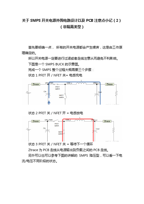
关于SMPS开关电源外围电路设计以及PCB注意点小记(2)(非隔离类型)首先要明确一点,所有的开关电源都会产生噪声,这是由工作原理确定的。
所以开关电源一定要进行过滤或者走线注意从而避免不利影响。
下图是一个SMPS BUCK的示意图。
完成一个SMPS 整个过程大概需要三个步骤:状态1 PFET 开 / NFET 关= 电感充电状态2 PFET 关 / NFET开 = 电感放电状态3 PFET 关 / NFET 关 = 等待下一个循环Ztrace为PCB走线从电源输出到负载之间的PCB走线。
另外可以也可以参考下图的讲解的SMPS 降压型,可以看一下电流/电压不同阶段的状态。
对于我们应用工程师来讲,我们无法改变IC内部SMPS选件以及设计状态,在不考虑SMPS内部设计本身的情况下。
如何发挥此IC SMPS最大效率和最小对外部干扰等影响的方法,以下有几个地方在设计电路器件选型和layout布线过程中需要注意:原理:上述红线和蓝线的动作部分是SMPS产生干扰和峰值的关键环节。
所以要保证一个低阻抗的环路无论是效率还是产生干扰来讲都是很有效的方式。
方法:器件的选型以及PCB走线:1.外部的功率电感。
首先一定是要根据负载的大小进行电感值的选择,一般参考电路都会根据IC的最大负载提供所需的标称电感值。
功率电感值不是越大越好。
好处:电感值越大电压纹波越小。
坏处:带载能力就降低,原因就是要得到同样带载能力,就要求输入电压越高。
根据上图状态1的充电电路,当PFET打开时,加在电感上的电压是输入电压与输出电压的差值。
电感越大,流过电感的电流增加得越慢,同样负载要得到同样的电流,需要的占空比越大。
在开关频率一定的情况下,占空比的增大是有限的,占空比耗在电感上,当负载增大时,就不能有足够的占空比来保证输出电压不下降了。
选取RDC直流电阻越小越好,效率会越高。
由于感值基本是SPEC已经规定的了,所以我们更加关注的是饱和电流。
一般选取最大负载电流2倍的规格进行选取。
开关电源设计手册(看2遍就懂).pdf

开关电源设计⼿册(看2遍就懂).pdf 反激式开关电源变压器设计计学习培训教材反激式开关电源变压器设计(2)⼀、变压器的设计步骤和计算公式:1.1 变压器的技术要求:输⼊电压范围;输出电压和电流值;输出电压精度;效率η;磁芯型号;⼯作频率f;最⼤导通占空⽐Dmax;最⼤⼯作磁通密度Bmax;其它要求。
1.2 估算输⼊功率,输出电压,输⼊电流和峰值电流:1)估算总的输出功率:P o=V01x I01+V02x I02……2)估算输⼊功率:P in= P o/η3)计算最⼩和最⼤输⼊电流电压V in(MIN)=AC MIN x1.414(DCV)V in(MAX)=AC MAX x1.414(DCV)技术部培训教材反激式开关电源变压器设计(2)4)计算最⼩和最⼤输⼊电流电流I in(MIN)=P INx VIN (MAX)Iin(MAX)=PINx VIN (MIN)5)估算峰值电流:K POUTI PK = VIN (MIN)其中:K=1.4(Buck 、推挽和全桥电路)K=2.8(半桥和正激电路) K=5.5(Boost ,Buck- Boost 和反激电路)技术部培训教材反激式开关电源变压器设计(2)1.3 确定磁芯尺⼨确定磁芯尺⼨有两种形式,第⼀种按制造⼚提供的图图表表,,按按各各种种磁磁芯芯可传递的能量来选择磁芯,例如下表:表⼀输出功率与⼤致的磁芯尺⼨的关系输出功率/W MPP环形E-E、E E--L L等等磁磁芯芯磁芯直径/(in/mm) (每边)/()/(in/mm)in/mm)<5 0.65(16) 0.5(11)5(11)<25 0.80(20) 1.1(30)1(30)<50 1.1(30) 1.4(35)4(35)<100 1.5(38) 1.8(47)8(47)<250 2.0(51) 2.4(60)4(60)技术部培训教材反激式开关电源变压器设计(2)第⼆种是计算⽅式,⾸先假定变压器是单绕组,每增加加⼀⼀个个绕绕组组并并考考虑安规要求,就需增加绕组⾯积和磁芯尺⼨,⽤“窗⼝利⽤⽤因因数数””来来修修整整。
开关电源设计软件SMPS Cal V5.0版

开关电源设计软件SMPS Cal V5.0版
SMPS Cal V5.0版本:
由于之前的版本采用从开关管耐压余量考虑,而且界面里面没有直观的反映最大占空比,折算电压等重要的参数,导致从耐压余量来设置参数很难放置到合理的数值,这也是导致很多人感觉结果偏差大,故V5.0加入了对反激变换器和RCC变换器采用图形界面来设参数,最大占空比,折算电压可以任意按一种方式设定,另外一个参数自动计算出来,而且耐压余量清楚的显示出来,这样可以很快得到想要的参数,但是需要提醒,输出电容的容量估计不是很准确,因为其采用的经验公式计算。
界面如下图:
界面红色文字部分是有设置对话框,点击打开即可设定,紫色的为调。
反激式开关电源变压器设计—Fairchild_资料
By Choi Blue cell is the input parametersRed cell is the output parameters6. Determine the numner of turns for each outputsVo VF # of turnsFPS Design Assistant ver.1.0Vcc (Use Vcc start voltage)1st output for feedback2nd output3rd output4th output5th output6th outputAL value (no gap)2Gap length (center pole gap)=7. Determine proper wire for each output Parallel Irms (A/mm 2)Primary winding0.5mm 1T 0.7A Vcc winding0.3mm 1T 0.1A 1st output winding0.4mm 4T 3.4A 2nd output winding0.4mm 4T 0.0A 3rd output windingmm T #DIV/0!A 4th output windingmm T #DIV/0!A 5th output windingmm T #DIV/0!A 6th output windingmm T #DIV/0!A Copper area =5.6584mm 2Fill factor0.2Required window area 28.292mm 28. Determine the rectifier diodes in the secondary side9. Determine the output capacitorESR Current Voltage ripple Ripple 1st output capacitor1000uF 50mΩ 2.7V 0.3V 2nd output capacitor1000uF 40mΩ0.0V 0.0V 3rd output capacitoruF mΩ#DIV/0!V #DIV/0!V 4th output capacitoruF mΩ#DIV/0!V #DIV/0!V 5th output capacitoruF mΩ#DIV/0!V #DIV/0!V 6th output capacitoruF mΩ#DIV/0!V #DIV/0!V Capacitance#DIV/0!#DIV/0!#DIV/0!6.70.0#DIV/0!Diameter 3.51.4(In Normal Operation)11. Design Feedback control loopControl-to-output DC gain =Control-to-output zero =Control-to-output RHP zero =Control-to-output pole =Voltage divider resistor (R1)Voltage divider resistor (R2)Opto coupler diode resistor (RD)431 Bias resistor (Rbias)Feeback pin capacitor (CB) =Feedback Capacitor (CF) =Feedback resistor (RF) =Feedback integrator gain (fi) =Feedback zero (fz) =Feedback pole (fp) =最小AC电压最大AC电压AC 主频率输出电压1输出电压2输出电压3输出电压4输出电压5输出电压6最大输出功率Po=Vo*I036效率最大输入功率Pin=Po/Eff45输入滤波电容纹波电压Vdcripple=?最小直流电压最大直流电压Vdcmax=1.414*Vacmax374.71最大占空比MOS管电压值Vds=Vdcmax+Vor455.71反射电压Vor=Dmax/(1-Dmax)*Vdcmin81工作频率功率因素Iripple=2*Iedc*Krf0.808081主电感量L=(Vdcmin*Dmax)2/(2*Pin*f*Krf)848.1635最大峰值电流Ip=Iedc+Iripple/2 1.414141Irms=sqrt(3*Iedc2+(Iripple/2)2*Dmax/3)681.8182Iedc=Pin/Dmax/Vdcmin 1.010101 L=Vdcmin*Dmax/(f*Iripple)848.2483 0.6954270.696003。
大功率开关电源、SMPS板,它包括原理图、PCB板丝印图、物料清单(BOM)、工程参数、承认书等
These drawings and specifications are the property of A&D World Company and shall not be reproduced or copied, or used as the basis for the manufacture or sale of apparatus or devices without permission.All Revision Seet 1Page No. 1 OF 1 SMPS A&D Code :-Engineering Change Notice - RecordRevision Number Date Signature RevisionDescription0 30.AUG.2006 HT Oh (A&D) FIRST ISSUETF Code Description Vender Type A53-PBD99KSP196-R-2 SMPS MODULE 150W KSP196F, KWANGSUNG KSP196F* Remark – Approval for TMS onlyVender : KWANG SUNGSPECIFICATIONFORAPPROVALDATE :株式會社KWANG SUNG ELECTRONICS CO.,LTD.108, 4-KA, WONHYO-RO, YONGSAN-KU, SEOUL, KOREA KWANG SUNG ELECTRONICS H.K CO.,LTD.UNIT8-9, 13/F, WAH WAI IND. CENTRE, 38-40AU PUI WAN ST., FO TAN, N.T., HONG KONGSHEN ZHEN KWANG SUNG ELECTRONICS CO.,LTD.BULDING #8, 5TH INDUSTRIAL ZONE,SHI YAN TOWN, BAO AN, SHEN-ZHEN, CHINATEL : 852-2602-6609 FAX : 852-2602-6490CHINA FACTORYTEL : 86-755-2763-3001/2FAX : 86-755-2763-3530TEL : 82-2-711-2001/5FAX : 82-2-712-8910HONG KONG OFFICE MODELKSP196U-1115004-02006.08.24HEAD OFFICE CUSTOMER'S APPROVALMESSRS :A&D WORLDITEMSwitched-Mode Power Supply(SMPS)光星電子1.1 HISTORY OF CHANGEAny change effecting manufactured or purchased parts, performanceinterchangeability,spare, or other reestablished routine and procedures or thephysical assembly must receive customer's written approval prior to in corporation.DATE CONTENT OF CHANGE PREPARE APPROVAL REV. NOKWANG SUNG ELECRONICS CO., LTD.This is special specification which differs from our standard specification for customer.1. ELECTRICAL CHARACTERISTICSI T E M DESCRIPTION2.THE OTHERSI T E M DESCRIPTIONKWANG SUNG ELECRONICS CO., LTD.(SPEC-0000)page 3page 6page 1page 7page 4MESSRS : A&D WORLDpage 9page 8page 5page 2MODEL :KSP196U-1115004-0 SPECIFICATION KP CODE :S M P S DATE : 2006.08.24PKSP196U-1115004-0DRAWDESIGN APPROVECHECKSPECIFICATION1 SCOPE2 AC INPUT REQUIREMENTS3 DC OUTPUT CHARACTERISTICS4 SEQUENCING REQUIREMENTS5 ENVIRONMENTAL REQUIREMENTS6 MECHANICAL REQUIREMENTS7 MARKING8 RELIABILITY9 OUTPUT CONNECTION SPEC10 PART LIST11 SCHEMATIC DIAGRAM12 DRAWINGKWANG SUNG ELECRONICS CO., LTD.01 SCOPEThis is defined the specification of KSP196U-1115004-0 SMPS by A&D WORLD.The specification defined the performance and characteristics of a open frame, single-phase, about Watts, 4 Output level power supply.+A A A W +A A A W +A A A W +A A A W W2 AC INPUT REQUIREMENTS2.1 Input Voltagea. Standard(Normal) input voltage : AC 110Vb. Standard(Normal) input frequency : 60Hz / 50Hzc. Input voltage range : AC 84 ∼ 134Vd. Input frequency range : 47Hz ∼ 63Hze. Input RangeRange : Min AC 84V Nor AC 110V Max 134V Current Max 4.5A2.2 Inrush Current.Maximum Inrush Current shall be less than 50 AMP-peak at full load and 25℃ambient cold start2.3 Efficiency (25℃)70% (Min), at normal input and maximum continuous load.KWANG SUNG ELECRONICS CO., LTD.PAGE 2TOTAL Watts(MAX)204.402.00 5.00200.00"40V DC 0.100.100.20 2.40"12V DC 0.010.100.100.50"5VS DC 0.01204.4Output voltageMin.load Nor.load Max.load Watts(MAX)Remark 5VA DC 0.010.100.30 1.50"3 DC OUTPUT CHARACTERISTICS3.1 The regulation shall be within limits under any combination of line, load, temperature, frequency, ripple voltage, warm-up drift, manufacturetolerrance.3.2 The specification ripple & noise are measured differently at the supplyusing maximum loads that are each shunted by 47uF electrolytic capacitor and 0.1uF ceramic capacitor.Measurements shall be made by using a storage Oscilloscope having a band width of 20MHz.3.3 Voltage, Current, Regulation, Ripple & Noise+DC A A A ∼+DC A A A ∼+DC A A A ∼+DC A A A ∼ 4 SEQUENCING REQUIREMENTS4.1 Reset After Shut DownIf the power supply latches into fold back or shut down state due to a fault condition on its outputs (over current or short circuit), the power supply sharp return to normal operation only after fault has been removed.4.2 On / Off Cyclewhen the supply is turn off for a minimum of 1.0 sec.4.3 Hold-up TimeHold-up shall be 20ms minimum at nominal input voltage of 110VAC withmaximum ouput load.4.4 Over ShootAny over shoot at turn on shall be less than 10% of the nominal voltage value. KWANG SUNG ELECRONICS CO., LTD.PAGE 338.0042.005.000.10 4.75 5.250.2011.4012.600.30 4.75 5.255VS 0.010.10Nominal OutputLoad Current(A)Tolerance Min.load Nor.load Max.load Ripple & Noise(MAX LOAD(230V/50Hz)150150300150mVp-p mVp-p mVp-p mVp-p 0.1040V 0.10 2.005VA 0.010.1012V 0.015 ENVIRONMENTAL REQUIREMENTSThe power supply shall be capable of performing its specified functions underenvironmental conditions specified in this document.5.1 Temperature Rangea. Operating Temp. : 0℃ ∼ 50℃b. Storage Temp : -20℃ ∼ +75℃5.2 Humidity (non condensing)a. Operating Humidity : 20% ∼ 80%b. Storage Humidity : 10% ∼ 90%5.3 Burn-inAll power supplies shall be subjected to the burn-in process at 40℃ ±5℃ in atemperature controlled enviroment.Burn-in criterion shall be as follower :a. Temperature condition : 40℃ ±5℃b. Load conditon : Normal Loadc. Input voltage : AC 110Vd. Burn-in Time : 2 Hours5.4 Insulation Resistancea. Condition : Non Operatingb. Test Point : Primary to Secondaryc. Test Specification : Greater than 100㏁ at DC 500V5.5 Vibration TestThe power supply shall be subjected to the following conditions with unpackaged unit.No damage should occur as a result of this test.Non Operating : Sweep testa. Frequncy : 5 → 60 → 5Hz (breake point : 8.6Hz)b. Acceleration : 0.5Gc. Direction : X, Y and Zd. Time : each 10 minutesKWANG SUNG ELECRONICS CO., LTD.PAGE 45.6 AC Line Noise (Impulse Noise)The Power supply shall Operate normally when AC line noise is applied.a. Noise crest value : AC 1000Vb. Polarity : +, -c. Pulse width : 50ns, 400ns, 800ns, 1usd. Cycle : 10mse. Phase : 0˚ ∼ 360˚f. Mode : common, normalg. Time : 3 minutes5.7 Dielectric Withstand Voltage (Hi-Pot)a. Condition : non operatingb. Test Point : primary to secondaryc. Test Specification : AC 1200V, 10mA, 1 Minutes5.8 Voltage Dip Testa. Input Voltage : AC 220Vb. Dip condition : 1Cycle → 100%2Cycle → 50%3Cycle → 20%6 MECHANICAL REQUIREMENTSThe mechanical profile,material and finish requirements are shown in theattached drawing.Materal shall be entirely suitable for the intended use.Protective coating shall be used on all corrosion susceptible materials toprevent rust,corrosion,aeration or other reactions deleterious to the function or appearance of the unit.6.1 Size (over all) : 120mm(L) * 180mm(W) * 35mm(H)7 MARKINGThe power supply shall be legibly marked with UL, CSA and VDE or TUV monogram (after approved),manufacturer's name, model number, serial or lot number,revision number, manufacturing date code, via adhesive label,Also normal input voltage,current,wattage,frequency,output rating,and other to be necessary shall clearly identified.KWANG SUNG ELECRONICS CO., LTD.PAGE 58 RELIABILITY8.1 Mean Time Between FailureThe power supply shall meet a minute of 25,000Hours MTBF at 25℃ ambient based on MIL HDBK 217-D8.2 WarrantyThe power supply shall be warranted for deafest involving workmanship, to include parts and labor, for a period of not less than 6 months from the original date of delivery.8.3 Quality AssuranceThe power supply shall be subjected to design review and performance verification as deemed necessary by the customer's quality organization and engineering organization.9 CONNECTION & OUTPUT PIN ASSIGNMENTKWANG SUNG ELECRONICS CO., LTD.PAGE6GND 40V 40V812 91110CN2GND CN3GND 6712V GND 455VS 5VD 23CON(H)P/D 1PIN NO。
开关电源(SMPS)的拓扑结构(第一部分)
前馈控制
在降压转换器中,输入电压变化在电压输出端产生的影 响通常可通过输入电压前馈控制降到最低。与模拟控制 方式相比,使用具有输入电压检测功能的数字信号控制 器能轻易实现前馈控制。在前馈控制方法中,数字信号 控制器一旦检测到输入电压的变化,在输入变化对输出 参数造成实际影响之前就将开始采取自适应措施进行相 应的处理。
AN1114
开关电源 (SMPS)的拓扑结构 (第一部分)
作者: Mohammad Kamil Microchip Technology Inc.
简介
工业驱动向更小、更轻和更高效的电子设备的发展趋势 促 进 了 开 关 电 源 (Switch Mode Power Supply, SMPS)的发展。通常可采用几种不同的拓扑结构实现 SMPS。
DS01114A_CN 第 2 页
2008 Microchip Technology Inc.
图 2:
(A)
降压转换器 IIN
Q1 VIN
D1
L
+ IL -
IOUT VOUT
AN1114
(B) Q1GATE
t
(C)
VL
VIN - VOUT
t
-VOUT
(VIN - VOUT)/L
(D)
IIN
t
-VOUT/L IL2
输入和输出电容的设计取决于每一个转换器的开关频率 乘以并联转换器的个数。从输出电容的角度来看纹波电 流减少 “n”倍。与图 2 (D)中所示的单一转换器相 比,多相同步降压转换器汲取的输入电流是连续的且纹 波较少,如图 3 (E)所示。因此,对于多相同步降压 转换器来说,较小的输入电容能满足设计要求。
电路设计之开关电源设计
1绪论开关电源(Switching Mode Power Supply,英文缩写为SMPS)又称为开关稳压电源,问世后在很多领域逐步取代了线性稳压电源和晶闸管相控电源。
随着全球对能源问题的越来越重视,电子产品的耗能问题将愈来愈突出,如何降低其待机功耗,提高供电效率成为一个急待解决的问题。
传统的线性稳压电源虽然电力结构简单、工作可靠,但它存在着效率低(只有40%〜50%)、体积大、铜铁消耗量大,工作温度高及调整范围小等缺点。
为了提高效率,人们研究出了开关式稳压电源,它的效率可达85% 以上,稳压范围宽;除此之外,还具有稳压精度高的特点,是一种较理想的稳压电源。
开关电源具有效率高、体积小、重量轻、应用广泛等优点,现已成为稳压电源的主流产品。
正因为如此,开关电源被誉为高效、节能型电源,代表着稳压电源的发展方向,并已广泛应用于各种电子设备中⑴。
1.1 开关电源的特点1.1.1 开关电源的优点(1) 功耗小,效率高。
晶体管V在激励信号的激励下,它交替地工作在导通一截止和截止一导通的开关状态,转换速度很快,频率一般为50kHz左右,在一些技术先进的国家,可以做到几百或者近1000kHz。
这使得开关晶体管V的功耗很小,电源的效率可以大幅度地提高,其效率可达到80%。
(2) 体积小,重量轻。
采用高频技术,省掉了体积笨重的工频变压器。
由于调整管V上的耗散功率大幅度降低后,又省去了较大的散热片。
由于这两方面原因,所以开关稳压电源的体积小,重量轻。
(3) 稳压范围宽。
从开关稳压电源的输出电压是由激励信号的占空比来调节的,输入信号电压的变化可以通过调频或调宽来进行补偿。
这样,在工频电网电压变化较大时,它仍能够保证有较稳定的输出电压。
所以开关电源的稳压范围很宽,稳压效果很好。
此外,改变占空比的方法有脉宽调制型和频率调制型两种。
开关稳压电源不仅具有稳压范围宽的优点,而且实现稳压的方法也较多,设计人员可以根据实际应用的要求,灵活地选用各种类型的开关稳压电源。
T807 T808 SMPS 电源电路设计文档说明书
B8.2.44T807/808 PCB InformationM800-0031/08/96Copyright TEL123456789123456789AB C D E F G H J KLMNPQRREV/ISS AMENDMENTS DATEAPVD D.O.CHKD DRAWN NO.SHEETS:FILE NAME:TAIT ELECTRONICSIPN:FILE DATE:ISSUE:ID:.2.SC.PROJECT:DESIGNER:12T807/T808 SMPSSCHEMATIC807_5B 220-01183-0514/07/96B T800*R12180X 100X*Q1IRF830MTH7N50*C12390UF200560UF200’*FAN-40A12B*R82150ZT 120ZT*D15BYV28-200MUR440’*C13680ND 1U0D*C732200UF163300UF16SMPST807T808*D18BYV28-200MUR440’L7*C682200UF163300UF16’*C15220PV6KV 470PV6KV*R1722X 10X*C11390UF200560UF200’L4L5*Q2IRF830MTH7N50*C9390UF200560UF200’L84A ADDED SELF-HEALING OVER VOLTAGE PROTECTION.MC *C692200UF163300UF16’A UPDATED FROM T99 D.B.HP.J.K.J.H22/02/9001A UPDATED FROM ISSUE A DJW PJK JH 28/05/9002A UPDATED FROM ISSUE 01A (C/N:90/09-454)DJW PJK JH 19/09/9003A UPDATED FROM ISSUE 02A (C/N:91/01-46)DJW 15/02/9103B C/N 91/05-401MC *SMPST807T808*R81150ZT 120ZT*C702200UF163300UF16’*C712200UF163300UF16’*C722200UF163300UF16’*R1922X 10X5A UPDATED FROM ISSUE 4A (C/N: )DJW 01/03/94*C10390UF200560UF200’*C14680ND 1U0D*T5T4072T4080SMPS T807T808*F15AFUSE 8AFUSE5B CAD/WANG, UNICAD FETCHRBM 14/07/96*C10390U *C11390U *C12390U *C13680N PP*C14680N PP*C15220P*C682200U*C692200U*C702200U*C712200U*C722200U*C732200U*C9390U *D15BYV28-200*D18BYV28-20030CPQ90D43 30CPQ90D43*FAN 12V FAN*F15A SLO BLOG DS *Q1IRF830 G DS*Q2IRF830*R12100*R1722*R1922*R81150*R82150*T5T4072C14N7TC161U0C17470PC18680PC1910NC24N7C201N0 C2147NC2247NC2347U HT C241U0 HTT C2510UC261N0C271N0 C3680NC311N0 C321N0C3347NT C3410UC351N0 C372200U HTC3847NC3947NC4680NC421N0 C431N0T C441U0C451N0C461N0C4947NC5T C5010UC511N0 C541N0C5547NT C5610UT C5710UC591N0C6C6047NT C6110UC6247NC631U0C65470UC664N7 PPC674N7 PP C742N2C752N2C78820UC7947NC801N0C811N0C821N0C8447NC8533P C861N0C872N2C8847NC8922PC901N0C911N0C951N0C96100N T C9810UC9922P D1MR756D111N4531D121N4531 D13GREEND14BYV26CD19BYV26CD2MR756D201N4531D211N4531D22BAT85 D23RED D241N4001 D251N4001D261N4001D271N4001D3MR756D301N4001D315V6 D32REDD361N4531D371N4531D381N4531D4MR756D411N4531D51N4531D61N4531 D71N4531D81N4531+-IC1358 567+-IC1358 321IC1358 V-4V+8VREG IC27815CTVIN 1GND2VOUT3+-IC3358321+-IC3358567IC3358 V-4V+8OUT -CHAR START IN OSC SYNCRTCTDIS SDGND VC VCC VREF SOFT OUT-AN.I.INOUT-BINV COMPIC4352543657101213151681121419IC542627IC542645IC5426 V-3V+6IC642627IC642645IC6426 V-3V+6IC7250VAC 4251IC8TL431213L1RFI FILTER2314L2500UH1423L32MH1423L6R F I F I L T E R2314PL-12 WAY PLUGPL-22 WAY PLUGQ10BC547Q11BC547Q12BC547 Q13BC547Q3BC557Q4BC547Q6BC337 Q7BC557Q8BC557 Q9BC337RLY1DPDTRLY1DPDT CWRV25470 231CW RV8110K231CW RV92470 231R110MGR10056KR10156K R102470K R10356KR10410KR1051K0R11100 R13A 68R13B 1K5 R141K5R181K2 VR2275VACR201K2 R241K2R26680R271K8 R28820R292K7R310R3010K R32100KR331K0 R3410K R3510KR3615KR371M0R3810KR393K9R447K R408K2 R416K8R4347KR4410KR45100KR4610KR4722R4815K VR49140VACR5270KR502K2R5110K R52180KR5333K R54B33K-TR5510KR5610KR5727KR5810KR591M0R6390KR6010K R611M0R626K8R6333R6422 R651K5R661K5R6710KR68100KR69680 R747K R70270R713K3 R7210R7310K R744K7 R754K7R766K8R79A 10R79B10 R868K R801K0R80A 10R80B 1K8 R8322R8422R8510MGR8647KR87100 R881K0R894K7R947KR9047KR911K0R93820 R941K2 R9568KR966K8R9810KR991K0SK-12 WAY SKTSK-22 WAY SKTSK-33 WAY SIDE ENTRY IEC SKTSK-4 1 WAY SIDE ENTRY TERMSK-5 SK-61 WAY SIDE ENTRY TERM SK-7 1 WAY SIDE ENTRY TERMSK-81 WAY SIDE ENTRY TERM 115V230V SW1DPDT115V230V SW1DPDTSW2SPST12TAB-1TC1THERMAL CUTOUTTP1TP2TP3TP42 WAY PLUGTP5TP6TP7T1T4073123412161467T2T4074 1256T3T4075123456T4T40795218610T6T40711I/OPAD2I/OPADP L -1P L -1PL-2PL-2S K -1S K -1SK-2SK-2SK-3EARTH2SK-3NEUTRAL1SK-3PHASE3TP42TP41VREFVREFVREF15V15V15V15V15V15V15V-OUT 15V-OUT15V-OUTCONTROL LOOP STABILIZATIONERROR AMP. + REFERENCEEMI MAINS FILTERSOFT STARTPOWER MOS DRIVEREMOTESENSEOUTPUT V-SETCURRENT LIMITC-LIMIT SETFAN CONTROL-+-+-++-POWER ONUNDERVOLTAGE LOCKOUTSTANDBYPLEASE NOTE:*COMPONENTS SHOWN ON CIRCUIT DIAGRAM ARE FOR T807YYYY XXY YYY Y105C Y IS CONNECTED BETWEEN MAINS & EARTH.X IS CONNECTED ACROSS THE MAINS.(X & Y CAPACITORS ARE REQUIRED TO MEET SAFETY REGULATIONS).4S34S34S34S3OUTPUT FILTERYYMAINS/PS FAIL ALARMPOWER SWITCHING(OPTIONAL ON T807)OUTPUT 13.8V+-1 WAY SIDE ENTRY TERMYYOVER VOLTAGEOVER C URRENTOVER C URRENTO/V ADJ.NOISEMODULATORNOTE: SHEET 2 CONTAINS NON-RELEVANT DATA4N74N71232。
- 1、下载文档前请自行甄别文档内容的完整性,平台不提供额外的编辑、内容补充、找答案等附加服务。
- 2、"仅部分预览"的文档,不可在线预览部分如存在完整性等问题,可反馈申请退款(可完整预览的文档不适用该条件!)。
- 3、如文档侵犯您的权益,请联系客服反馈,我们会尽快为您处理(人工客服工作时间:9:00-18:30)。
开关电源设计手册目录1 隔离式电源设计1.1 有源功率因数校正1.2 反激式电源设计1.3 正激式电源设计2 非隔离式电源设计2.1 非隔离式降压型电源设计1.1 有源功率因数校正APFC: Active Power Factor Correction一, 功率因数校正的基本原理理论上: P.F.= P/S=(REAL POWER)/(TOTAL APPARENT POWER)=Watts/V.A.=有功功率/视在功率对于输入电压和电流都是理想的正弦波的情况, 如果把输入电压和输入电流的相位差定义为φ, 那么, P.F.=P/S=Cosφ. 相应的功率相量图如下:对于非理想的正弦波, 假设输入电压为正弦波, 输入电流为周期性的非正弦波, 比如在实际的AC-DC线路中广泛应用的全波整流, 只有当输入电压大于电容的电压时, 才有市电电流给电容充电.在这种情况下, 电压有效值Vrms=Vpeak/√2周期性的非正弦波电流经过傅里叶变换为:(Io: 电流直流分量; I1RMS: 电流基波分量, 頻率与V相同; I2RMS….I nRMS: 电流谐波分量, 频率为基波的2….n 倍. )对于纯净的交流信号, Io=0; I1RMS基波分量有一个同向成份I1RMSP和一个求积成份I1RMSQ.于是电流有效值可以表达为:有功功率P=V RMS*I1RMSP=V RMS*I1RMS*Cosφ1(φ1: 输入电压和输入电流基波分量I1RMS的相位差)S=V RMS*IRMS total于使功率因数Power Factor 可以表达为:P.F.=P/S= (I1RMS/I RMS total)* Cos φ1;定义电流失真系数K= I1RMS/I RMS total = Cosθ; θ为失真角(Distortion angle); K 为与电流谐波(Harmonic) 分量有关的系数. 如果总的谐波分量为零, K 就为1.最后, 可以表达为: P.F.=Cos φ1*Cos θ ; 功率向量图如下:φ1 是电压V与电流基波I1RMS之间的相量差;θ是电流失真角;可见功率因数 (PF) 由电流失真系数 ( K ) 和基波电压、基波电流相移因数( Cos φ1) 决定。
Cos φ1低,则表示用电电器设备的无功功率大,设备利用率低,导线、变压器绕组损耗大。
同时,K值低,则表示输入电流谐波分量大,将造成输入电流波形畸变,对电网造成污染,严重时,对三相四线制供电,还会造成中线电位偏移,致使用电电器设备损坏。
由于常规整流装置常使用非线性器件(如可控硅、二极管),整流器件的导通角小于180o,从而产生大量谐波电流成份,而谐波电流成份不做功,只有基波电流成份做功。
所以相移因数(Cos φ1)和电流失真系数(K)相比,输入电流失真系数(K)对供电线路功率因数 (PF) 的影响更大。
为了提高供电线路功率因数,保护用电设备,世界上许多国家和相关国际组织制定出相应的技术标准,以限制谐波电流含量。
如:IEC555-2, IEC61000-3-2,EN 60555-2等标准,它们规定了允许产生的最大谐波电流。
我国于1994年也颁布了《电能质量公用电网谐波》标准(GB/T14549-93)。
二, PF与总谐波失真系数(THD: Total Harmonic Distortion)的关系三.功率因数校正实现方法由功率因数: P.F.=Cos φ*K = 1可知,要提高功率因数,有两个途径:1.使输入电压、输入电流同相位。
此时Cos φ =1, 所以PF=K2.使输入电流正弦化。
即I RMS=I1RMS(谐波为零),有I1RMS/IRMS=1 , 即P.F.=Cos φ*K = 1从而实现功率因数校正。
利用功率因数校正技术可以使交流输入电流波形完全跟踪交流输入电压波形,使输入电流波形呈纯正弦波,并且和输入电压同相位,此时整流器的负载可等效为纯电阻,所以有的地方又把功率因数校正电路叫做电阻仿真器.四, 有源功率因数校正方法分类1.按有源功率因数校正电路结构分(1)降压式:因噪声大,滤波困难,功率开关管上电压应力大,控制驱动电平浮动,很少被采用。
(2)升/降压式:需用二个功率开关管,有一个功率开关管的驱动控制信号浮动,电路复杂,较少采用。
(3)反激式:输出与输入隔离,输出电压可以任意选择,采用简单电压型控制,适用于150W以下功率的应用场合。
(4)升压式(boost):简单电流型控制,PF值高,总谐波失真(THD)小,效率高,但是输出电压高于输入电压。
适用于75W~2000W功率范围的应用场合,应用最为广泛。
它具有以下优点:•1电路中的电感L适用于电流型控制。
•2由于升压型APFC的预调整作用在输出电容器C上保持高电压,所以电容器C体积小、储能大。
•3在整个交流输入电压变化范围内能保持很高的功率因数。
•4输入电流连续,并且在APFC开关瞬间输入电流小,易于EMI滤波。
•5升压电感L能阻止快速的电压、电流瞬变,提高了电路工作可靠性。
UC3854, L4981是一种工作于平均电流的的升压型(boost)APFC电路,它的峰值开关电流近似等于输入电流,是目前使用最广泛的APFC电路。
2.按输入电流的控制原理分(1)平均电流型:工作频率固定,输入电流连续(CCM),波形图如图1(a)所示。
TI的UC3854, ST的L4981就工作在平均电流控制方式。
一般用于输出功率Po > 400~500W 的大功率场合 .这种控制方式的优点是:•1恒频控制。
•2工作在电感电流连续状态,开关管电流有效值小、EMI滤波器体积小。
•3能抑制开关噪声。
•4输入电流波形失真小。
主要缺点是:•1控制电路复杂。
•2需用乘法器和除法器。
•3需检测电感电流。
•4需电流控制环路。
(2)滞后电流型。
工作频率可变,电流达到滞后带内发生功率开关通与断操作,使输入电流上升、下降。
电流波形平均值取决于电感输入电流,波形图如图1(b)所示。
一般用于输出功率200W < Po < 400W 的中等功率场合.(3)峰值电流型。
工作频率变化,电流不连续(DCM),工作波形图如图1(c)所示。
一般用于输出功率Po < 250W 的小功率场合.DCM采用跟随器方法具有电路简单、易于实现的优点,但存在以下缺点:功率因数和输入电压V in与输出电压V O的比值Vin/Vo有关。
即当V in变化时,功率因数PF 值也将发生变化,同时输入电流波形随Vin/Vo的加大而THD变大。
开关管的峰值电流大(在相同容量情况下,DCM中通过开关器件的峰值电流为 CCM的两倍),从而导致开关管损耗增加。
所以在大功率APFC电路中,常采用CCM方式。
(4)电压控制型。
工作频率固定,电流不连续,工作波形图如图1(d)所示。
五, PFC的工作原理六, PFC的实际设计及应用下面以TI/UNITRODE 的UC3854; ST的L4981, L6561/L6562 为例进行讲解.A. 先以 TI / UNITRODE的UC3854为例进行说明.>>> UC3854 的特性:● Control Boost PWM to 0.99 Power Factor ●升压脉冲宽度调制,功率因数可达0.99 ● Limit Line Current Distortion To <5% ●市电电流谐波可达<5%● World-Wide Operation Without Switches ●宽市电电压, 不需选择开关● Feed-Forward Line Regulation ●前馈市电调节● Average Current-Mode Control ●平均电流控制● Low Noise Sensitivity ●低噪音敏感性● Low Start-Up Supply Current ●低启动工作电流● Fixed-Frequency PWM Drive ●固定的PWM驱动频率● Low-Offset Analog Multiplier/Divider ●低偏置电压的模拟乘/除法器● 1A Totem-Pole Gate Driver ● 1A 图腾柱门极驱动● Precision Voltage Reference ●精确的电压参考>>> UC3854的功能描述:它可以进行电源的功率因数校正, 防止电源从正弦电压市电吸取非正弦的电流, 充分利用从市电吸收的电流, 减小电流谐波. 为了达到这些功能, UC3854 包含:● a voltage amplifier ●一个电压放大器● an analog multiplier/divider ●一个模拟乘/除法器● a current amplifier ●一个电流放大器● a fixed-frequency PWM ●一个固定频率的PWM另外, 它还有:● a power MOSFET compatible gate driver ●一个与MOSFET兼容的门极驱动● 7.5V reference ● 7.5V 电压参考● line anticipator ●市电预期● load-enable comparator ●负载使能比较器● low-supply detector ●低电压侦测● over-current comparator ●过流比较器UC3854 利用平均电流控制方法, 跟峰值电流控制不一样的是, 平均电流控制可以精准的保持市电电流为正弦波, 并且不需要斜率补偿, 最小限度的对市电瞬态噪音作反应.它的高电压参考和大的震荡幅值可以减小对噪音的敏感度, 工作频率可达200KHz. 可用在单相和三相电源, 市电电压从75V到 275V, 频率从50Hz到 400Hz的范围. 为了减小工作所需能量,UC3854有低启动电流的特点.>>>UC3854的引脚功能:引脚号引脚符号引脚功能1 GND 接地端,器件内部电压均以此端电压为基准2 PKLMT 峰值限定端,其阈值电压为零伏与芯片外检测电阻负端相连,可与芯片内接基准电压的电阻相连,使峰值电流比较器反向端电位补偿至零3 CA out 电流误差放大器输出端,对输入总线电流进行检测,并向脉冲宽度调制器发出电流校正信号的宽带运放输出4 Isense 电流检测信号接至电流放大器反向输入端,4引脚电压应高于-0.5V(因采用二极管对地保护)5 Mult. out 乘法放大器的输出和电流误差放大器的同相输入端6 I AC乘法器的前馈交流输入端,与B端相连,(6)引脚的设定电压为6V,通过外接电阻与整流输出电压的正端相连.7 V A out 误差电压放大器的输出电压,这个信号又与乘法器A端相连,但若低于1V乘法器便无输出8 V RMS前馈总线有效值电压端,与跟输入线电压有效值成正比的电阻相连时,可对线电压的变化进行补偿9 V REF基准电压输出端,可对外围电路提供10mA的驱动电流10 ENA 允许比较器输入端,不用时与+5V电压相连11 Vsense 电压误差放大器反相输入端,在芯片外与反馈网络相连,或通过分压网络与功率因数校正器输出端相连12 Rset 12端信号与地接入不同的电阻,用来调节振荡器的输出和乘法器的最大输出13 SS 软启动端,与误差放大器同相端相连14 C T接对地电容器C T,作为振荡器的定时电容15 Vcc 正电源阈值为10V~16V16 GT DRV PWM信号的图腾输出端,外接MOSFET管的栅极,该电压被钳位在15V>>>UC3854 的控制方法:在APFC电路中,整流桥后面的滤波电容器移到了整个电路的输出端(见图2、图4中的电解电容C),这是因为V in应保持半正弦的波形,而V out需要保持稳定。