
菲尼克斯电气 MINI Analog隔离放大器产品系列
诺顺rs-1013系列单电源单配电隔离放大器使用手册说明书

RS-1013系列单电源单配电隔离放大器产品特点:典型应用:● 0-10mV/0-20mV/0-75mV/0-100mV 的小信号隔离放大● 精度等级:0.1、0.2级 ● 高线性度 <0.1%● 电源、信号输入/输出 3000VDC 三隔离 ● 辅助电源:12VDC 或24VDC 单电源供电● 提供两组隔离电源:5VDC~24VDC (缺省值为+12V )● 提供输入端+1.25V ,输出端+5V,精度±2%基准电源 ● 标准DIP-24,符合UL94V-0标准阻燃超小体积封装 ● 工业级温度范围: -20~+85 ℃● 模拟信号调理、隔离、采集和变换 ● 工业现场信号隔离及变换 ● PLC & FA 电机信号隔离控制 ● 工业现场地线干扰抑制● 仪器仪表与传感器信号隔离及变换 ● 非电量信号变送 ● 信号远程无失真传输● 电力监控、医疗设备隔离安全栅等概述:RS-1013是一种将模拟信号按比例隔离转换的混合集成电路。
该电路在同一芯片上集成了一组多路高隔离的DC/DC 电源和几个高性能的信号隔离器,特别适用于:0-10mV/0-20mV/0-75mV/0-100mV 的小信号放大。
该芯片的隔离电源除了为内部放大电路供电外,还可以向外(信号输入/输出端)提供两组隔离的直流电源和两个基准电压源,可供外部电路扩展用,如电桥电路、基准电路等。
SMD 工艺结构及新技术隔离措施使该器件能达到:电源、信号输入/输出 3000VDC 三隔离。
并且能满足工业级宽温度、潮湿、震动的现场恶劣工作环境要求。
RS-1013系列隔离放大器使用非常方便,只需很少外部元件,即可实现模拟小信号调理、隔离、采集和变换。
图1 原理框图 表1极限参数表极限参数特性:连续隔离电压值: 3000VDC电源电压输入范围:±20%Vin焊接温度(10秒):+300℃输出最小负载: 1K Ω备注:输入值超过上述范围可能会造成芯片永久性损坏使用说明输入4-20mA时,RS-1013典型接线图(图2)输入电压信号时,RS-1013典型接线图(图3)图2 电流输入典型接线图3 电压输入典型接线图4 测量高电压信号应用实例1:(参见图3)用隔离放大器直接测量低电压信号输入:0~100mVDC直流电压信号;输出:1~5VDC 隔离信号。
CA30CAN CAF 4TH 代三重保护电容接近传感器说明书
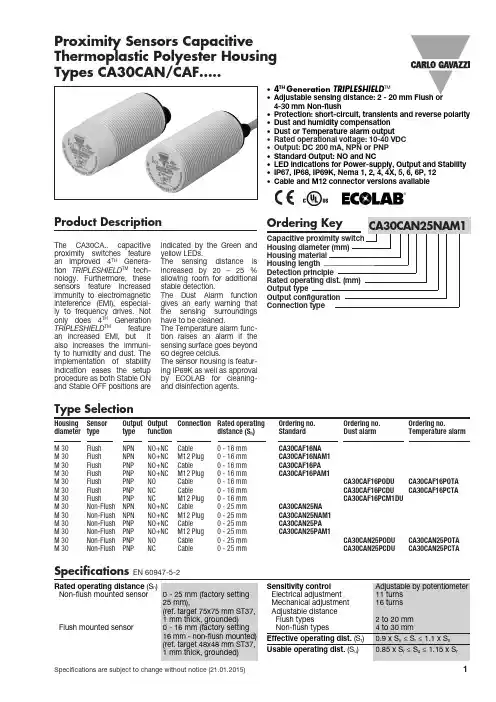
Proximity Sensors Capacitive Thermoplastic Polyester Housing Types CA30CAN/CAF.....• 4TH Generation TRIPLESHIELD TM• Adjustable sensing distance: 2 - 20 mm Flush or 4-30 mm Non-flush• Protection: short-circuit, transients and reverse polarity • Dust and humidity compensation • Dust or Temperature alarm output • Rated operational voltage: 10-40 VDC • Output: DC 200 mA, NPN or PNP • Standard Output: NO and NC• LED indications for Power-supply, Output and Stability • IP67, IP68, IP69K, Nema 1, 2, 4, 4X, 5, 6, 6P, 12• Cable and M12 connector versions availableProduct DescriptionThe CA30CA.. capacitive proximity switches feature an improved 4TH Genera-tion TRIPLESHIELD TM tech-nology. F urthermore, these sensors feature increased immunity to electromagnetic inteference (EMI), especial-ly to frequency drives. Not only does 4TH Generation TRIPLESHIELD TM feature an increased EMI, but it also increases the immuni-ty to humidity and dust. The implementation of stability indication eases the setup procedure as both Stable ON and Stable OFF positions are indicated by the Green and yellow LEDs.increased by 20 – 25 % allowing room for additional stable detection.gives an early warning that have to be cleaned.The Temperature alarm func-tion raises an alarm if the sensing surface goes beyond 60 degree celcius.The sensor housing is featur-ing IP69K as well as approval by ECOLAB for cleaning- and disinfection agents.Rated operating distance (S n ) Non-flush mounted sensor 0 - 25 mm (factory setting 25 mm), (ref. target 75x75 mm ST37, 1 mm thick, grounded) Flush mounted sensor 0 - 16 mm (factory setting 16 mm - non-flush mounted) (ref. target 48x48 mm ST37, 1 mm thick, grounded)Specifications EN 60947-5-2Housing Sensor Output Output ConnectionRated operating Ordering no. Ordering no. Ordering no.diameter type type function distance (S n ) StandardDust alarmTemperature alarmM 30 Flush NPN NO+NC Cable 0 - 16 mm CA30CAF16NA M 30 Flush NPN NO+NC M12 Plug 0 - 16 mm CA30CAF16NAM1M 30 Flush PNP NO+NC Cable 0 - 16 mm CA30CAF16PA M 30 Flush PNP NO+NC M12 Plug 0 - 16 mm CA30CAF16PAM1M 30 Flush PNP NO Cable 0 - 16 mm CA30CAF16PODU CA30CAF16POTAM 30 Flush PNP NC Cable 0 - 16 mmCA30CAF16PCDU CA30CAF16PCTA M 30 Flush PNP NC M12 Plug 0 - 16 mm CA30CAF16PCM1DUM 30 Non-Flush NPN NO+NC Cable 0 - 25 mm CA30CAN25NA M 30 Non-Flush NPN NO+NC M12 Plug 0 - 25 mm CA30CAN25NAM1M 30 Non-Flush PNP NO+NC Cable 0 - 25 mm CA30CAN25PA M 30 Non-Flush PNP NO+NC M12 Plug 0 - 25 mm CA30CAN25PAM1M 30 Non-Flush PNP NO Cable 0 - 25 mm CA30CAN25PODU CA30CAN25POTA M 30Non-FlushPNPNCCable0 - 25 mmCA30CAN25PCDU CA30CAN25PCTAType SelectionCA30CAN/CAF.....Specifications (cont.) EN 60947-5-2* The IP69K test according to DIN 40050-9 for high-pressure, high-temperature wash-down applications. The sensor must not only be dust tight (IP6X), but also able to withstand high-pressure and steam cleaning. The sensor is exposed to high pressure water from a spray nozzle that is fed with 80°C water at 8’000– 10’000 KPa (80–100bar) and a flow rate of 14–6L/min. The nozzle is held 100 –150 mm from the sensor at angles of 0°, 30°, 60° and 90° for 30s each. The test device sits on a turntable that rotates with a speed of 5 times per minute. The sensor must not suffer any damaging effects from the high pressure water in appear-ance and function.90°60°30°0°The environments in which capacitive sensors are in s tall e d can often be un s ta-ble as regards to tempera-ture, humi d ity , object dis-tance and industrial (noise) inter f erence. Because of this, Carlo Ga v azzi offers as standard features in all TRIPLESHIELD TM capacitive sensors a user-friendly sen-sitivity adjustment instead of a fixed sensing range. Likewise, these sensors provide an extend e d sen-sing range to accommodatemechanically de m and i ng are-as and tem p erature stability to en s ure high immunity to elec t ro m agnetic interference (EMI) and a minimum need for adjusting sensitivity if the temperature varies.Note:Sensors are factory set (default) to nominal sensing range S n .Adjustment GuideCA30CAN/CAF.....Wiring DiagramDetection DiagramCA30CAN/CAF.....Detection Stability IndicationDimensionsInstallation HintsCapacitive sensors have a unique ability to detect al-most any material in li q uid or solid form. Capa c i t ive sen-sors are able to detect me-tallic as well as non-metallic ob j ects. How e ver, their tradi-tional use is for non-metallic materials such as:• Plastics Industry Resins, regrinds or mould-ed products.• Chemical IndustryCleansers, fertilizers, liq-uid soaps, corrosives andpe t r o c hemicals.• Wood IndustrySaw dust, paper products,door and window frames.• Ceramics & GlassI ndustryRaw materials, clay orfinish e d products, bottles.• Packaging IndustryPackage inspection for lev-el or contents, dry goods,fruits and vegetables, dairyproducts.Materials are detected due totheir dielectric constant. Thebigger the size of an object,the higher the density of ma-terial, the better or easier it isto detect the object.The nominal sensing di s tan-ce for a capacitive sensoris refe r r ed to a groundedme t al plate (ST37). For addi-tional information regardingdi e lec t ric ratings of materi-als please re f er to TechnicalInformation.Relief of cable strain Protection of the sensing face Switch mounted on mobile carrier To avoid interference from inductive voltage/current peaks, separate the prox. switch pow-er cables from any other power cables, e.g.motor, contactor or solenoid cablesNot correctCorrectThe cable should not be pulled A proximity switch should not serve asmechanical stopAny repetitive flexing of thecable should be avoided Delivery Contents•Capacitive switch: CA30CAN/CAF.......• User manual• 2 x M30 fingernuts• Screwdriver• Packaging: Cardboard boxAccessories• Connector type CONM14NF.. -series.• Mounting Brackets AMB30-S.. (straight),AMB30-A.. (angled)CA30CAN/CAF.....。
美格尔新产品:DC电阻捕捉仪MIT515、MIT525、MIT1025和MIT1525说明书

DESCRIPTIONMegger’s new range of DC insulation testers MIT515, MIT525,MIT1025 and MIT1525 are targeted at original equipment manufacturers and industrial companies. The top of the rangeMIT1525 performs insulation resistance tests up to 15 kV with a30 TΩ maximum resistance and an accuracy of ±5 % from 1 MΩup to 3 TΩ. The MIT515 offers IR, DAR and PI functions but has no memory functionality. MIT525, MIT1025 and MIT1525 have a full suite of test modes as well as on-board memory and the ability to stream data/download data to a PC/laptop. Instrument productivity is a focus of the new MIT range which offers rapid charge batteries and operation from an AC source if the batteries are flat. Rapid charge batteries enable > 60 minutes testing after a 30 minute charge.MIT515: 5 kV IRT with PI and DAR but no memoryMIT525: 5 kV IRT with all test modes including a ramp test plus advanced memory functions with recall to screen, RTC for time/dat stamp of results and USB cable interface to PC/PowerDBMIT1025: 10 kV IRT with all test modes including a ramp test plus advanced memory functions with recall to screen, RTC for time/dat stamp of results and USB cable interface to PC/PowerDBMIT1525: 15 kV IRT with all test modes including a ramp test plus advanced memory functions with recall to screen, RTC for time/dat stamp of results and USB cable interface to PC/PowerDBSafety rating is not compromised on the MIT range with all terminals safety rated to CAT IV 600 V to 3000 m (5 kV, 10 kV) or CAT IV 1000 V to 3000 m (15 kV). A range of 5 kV and 10 kV test leads are available plus dedicated 15 kV test leads which are double insulated with clips designed for 15 kV creepage paths. The 15 kV leads are supplied in a holdall. Suitably rated HV gloves and other personal protection equipment are required to be worn when testing.The MIT range share dual case design which includes a tough outer case to protect the tester from knocks/drops and an inner fire retardant case. The IP rating is IP 65 case closed eliminating moisture and dust ingress.An intuitive user interface ensures no lost time remembering how to use the tester. Simplicity of operation is achieved with two rotary switches and the large backlight display which enables multiple results to be displayed simultaneously. A graphical quick start guide is provided inside the lid to assist first time users.Five preset voltage ranges are provided in insulation test mode, plus a user settable lock voltage range. Preconfigured diagnostic tests include Polarisation Index (PI), Dielectric Absorption Ratio (DAR), dielectric discharge (DD), Stepped Voltage (SV) and ramp test. Advanced memory storage includes time/date stamping of results, logging of data and recall of results to screen. A fully isolatedUSB interface is used for safe transfer of data to Megger’s asset management software; PowerDB Pro, Advanced and Lite packages.Test leads are double insulated t with clamps rated at 3 kV t equivalent to 6 kV single insulation for the medium clip leadset and 5 kV t equivalent to 10 kV single insulation for the large clip. The 15k V leadset is insulated to 15 kV.Advanced memory storage includes time/date stamping of results, logging of data and recall of results to screen. A fully isolated USBMIT515, MIT525, MIT1025, MIT15255 kV, 10 kV, 15 kV DC Insulation Resistance TestersMIT515, MIT525, MIT1025, MIT15255 kV, 10 kV, 15 kV DC Insulationresistance testers■■Measures up to 30 TΩ■■Safety rated up to CAT IV 1000 V to 3000 m■■Unique dual-case design - additional userprotection■■Operates from battery or AC mains supply■■Rapid charge Li-ion battery■■Advanced memory with time/date stampdevice interface (type B) is used for safe transfer of data to Megger’s PowerDB / Pro, Advanced and Lite asset management software. (MIT525, MIT1025 nd MIT1525 only)APPLICATIONThe Insulation Resistance (IR) test is a quantitative test which indicates the effectiveness of a product’s electrical insulation. Applications include cables, transformers, motors/generators, circuit breakers and bushings. Common insulation tests are the “spot test”, a 1 minute IR test and a 10 minute Polarisation Index (PI) test, where PI is the ratio R10min / R1min and is temperature independent.FEATURES AND BENEFITS■■Insulation resistance up to 30 TΩ @ 15 kV , 20 TΩ @ 10kV , 10 TΩ@ 5 kV■■IR, Timed IR, DAR, PI, DD, SV and ramp diagnostic tests ■■High current – 3 mA short circuit current■■High noise immunity – 3 mA (5 kV and 10 kV) 6 mA (15 kV) ofnoise rejection■■Li-ion battery – up to 6 hrs continuous testing @ 5 kV with a100M load, battery meets IEC 2133■■Safety rating: CAT IV 600 V to 3000 m (5 kV , 10 kV) CAT IV 1000V to 3000 m (15 kV)■■Large LCD display with backlight■■Dedicated voltmeter function (30 V to 660 V)■■Advanced memory, on screen recall and real time clock for date/time stamped results (MIT525, MIT1025 and MIT1525 only)■■Download of on-board results via USB interface (MIT525,MIT1025 and MIT1525 only)■■Recorded temperature (measured by independent instruments)can be saved with test result (MIT525, MIT1025 and MIT1525 only)■■PowerDB Lite asset management software supplied (MIT525,MIT1025 and MIT1525 only)■■MIT515, MIT525 and MIT1025 safety rated at CAT IV 600 V(maintained to 3000 m altitude)■■MIT1525 safety rated at CAT IV 1000 V (maintained to 3000 maltitude)SPECIFICATIONSAC voltage (auto-ranging)5 kV , 10 kV: 90-264 V rms, 47- 63 Hz 100 VA15 kV: 90-264 V rms, 47- 63 Hz 200 VABattery charge time 2.5 hours deep discharge, 2 hours normal dischargeBattery life11.1 V , 5.2Ah Li-ion batteries, meet IEC 62133:2003, MIT1525 has 2 battery packsBattery life MIT515, MIT525: 6 hours (typical) continuous testing at 5 kV with a 100 MΩ load Battery life MIT1025: 4.5 hours (typical) continuoust esting at 10 kV with a 100 MΩ load Battery life MIT1525: 4.5 hours (typical) continuous t esting at 15 kV with a 100 MΩ load Test voltageMIT515, MIT525:250 V , 500 V , 1000 V , 2500 V , 5000 V , V L MIT1025:500 V , 1000 V , 2500 V , 5000 V , 10000 V , V L MIT1525:1000 V , 2500 V , 5000 V , 10000 V , 15000 V , V L Lock test voltage100 V L to 1 kV in 10 V steps, 1 kV to 5 kV in 25 V steps, 5 kV to 15 kV in 25 V steps Test voltage accuracy+4%, -0%, ±10 V nominal test voltage at 1 GΩ load (0°C to 30°C)Resistance range10 kΩ to 15 TΩ @ 5 kV , 10 kΩ to 20 TΩ @ 10 kV , 10 kΩ to 30 TΩ @ 15 kVAccuracyMIT515, MIT525 accuracy (23 °C) 5000 V 2500 V 1000 V 500 V250 V±5% from 1MΩ to 1 TΩ 500 GΩ 200 GΩ 100 GΩ 50 GΩ ±20% from 1MΩ to 10 TΩ 5 TΩ 2 TΩ 1 TΩ 500 GΩ MIT1025 accuracy (23 ºC) 10 kV 5000 V 2500 V 1000 V500 V±5% from 1MΩ to 2 TΩ 1 TΩ 500 GΩ 200 GΩ 100 GΩ±20% from 1MΩ to 20 TΩ 10 TΩ 5 TΩ 2 TΩ1 TΩMIT1525 accuracy (23 ºC) 15 kV 10 kV 5000 V 2500 V 1000 V ±5% from 1MΩ to 3 TΩ 2 TΩ 1 TΩ 500 GΩ 200 GΩ±20% from 1MΩ to 30 TΩ20 TΩ10 TΩ5 TΩ2 TΩGuard terminal performanceGuards out parallel leakageresistance down to 250 kΩ with a maximum additional resistance error of 1% with a 100 MΩ load DisplayAnalogue : 100 kΩ to 10 TΩDigital: 10 kΩ to max a above Short circuit/charge current 3 mA @ 5 kV , 10 kV , 15 kV Insulation testAlarm: 100 kΩ to 10 GΩTEST LEADS SUPPLIEDThe MIT515. MIT525, MIT1025 and the MIT1525 are all supplied with test leads that are compliant with the requirements ofIEC61010-031:2008. The 5 kV models are supplied with one 3m lead-set with medium sized clips. The 10 kV models are supplied with two 3m lead-sets, one with medium sized clips and the other with large clips with insulation suited to 10 kV use and the 15 kV models supplied with a 3m lead-set, with large clips with insulation suited to 15 kV use.These leads are designed based on Megger’s extensive knowledge of insulation testing using the latest technology. The leads are in compliance with IEC61010-31:2008 which requires a fully insulated clip design.MEDIUM INSULATED TEST CLIP 3 M X 3 LEADSET - 5 KV AND 10 KVThese test leads are supplied as standard on MIT515, MIT525 and the MIT1025.These clips are designed for clamping on larger diameter test pieces but where space is at a premium.The insulation is designed only to protect the user from the output of Megger 5 kV and 10 kV (set below 6 kV) insulation resistance testers. The clips cannot in any circumstance be relied on to protect the user from live ac systems above 600 V a.c., r.m.s. in an CAT IV environment.Cable insulation rating: 12 kV dc (marked on cable)Cable type: flexible dual insulated silicon (inner insulation layer coloured white tohighlight damageCapacitor chargeMIT515, MIT525 <3 s/μF at 3 mA to 5 kV MIT1025 <5 s/μF at 3 mA to 10 kV MIT1525 <7.5 s/μF at 3 mA to 15 kV Capacitor discharge<120 ms/μF to discharge from 5000 V to 50 V (MIT515 and MIT525)<250 ms/μF to discharge from 10000 V to 50 V (MIT1025)<3500 ms/μF to discharge from 15000 V to 50 V (MIT1525)Capacitance range With test voltage set above 500 VMIT515, MIT525 MIT1025: 10 nF to 25 μF MIT1525: 10 nF to 50 μFCapacitance measurement accuracy ±10% ±5 nF Current range 0.01 nA to 6 mACurrent accuracy ±5% ±0.2 nA at all voltages (23 °C)InterferenceMIT515, MIT525: 3 mA from 450 V to 5 kV MIT1025: 3 mA from 960 V to 10 kV MIT1525: 6 mA from 2100 V to 15 kV Voltmeter range 30 V to 660 V ac or dc, 45Hz – 65Hz Voltmeter accuracy ±3%, ±3VTimer range Up to 99 minutes 59 seconds, 15 second minimum setting Memory capacity5.5 hours logging @ 5 sec intervals(MIT525, MIT1025 and MIT1525 only)Test modesMIT515: IR, IR(t), DAR, PIMIT525, MIT1025 and MIT1525: IR, IR(t), DAR, PI, SV , DD, ramp testInterfaceUSB type B (device)(MIT525, MIT1025 and MIT1525 only)Real time output1 Hz output readings (V , I, R) (MIT525, MIT1025 and MIT1525 only)ENVIRONMENTAL Maximum altitude3000 m (5 kV , 10 kV)3000 m (15 kV)Operating temperature range -20 °C to 50 °C Storage temperature range -25 °C to 65 °CHumidity 90% RH non-condensing at 40 °C IP rating IP65 (lid closed), IP40 (lid open)SAFETYMIT515, MIT525 MIT1025: CAT IV 600 V to 3000 m altitude MIT1525: CAT IV 1000 V to 3000 m altitude Meets the requirements of IEC 61010-1,TEST LEADS SUPPLIED CONT.MEDIUM INSULATED TEST CLIP 3 M X 3 LEADSET - 15 KVThese test leads are supplied as an option on the MIT1525.These clips are designed for clamping on larger diameter test pieces but where space is at a premium.The insulation is designed only to protect the user from the output of Megger 15 kV (set below 6 kV) insulation resistance testers.The clips cannot in any circumstance be relied on to protectthe user from live ac systems above 1000 V a.c., r.m.s. in an CAT IV environment.Cable insulationrating: 15 kV dc(marked on cable)Cable type: flexibledual insulated silicon(inner insulation layercoloured white tohighlight damage These test leads may also be supplied in none standard lengths to suit a particular application.Please contact Megger for a quotation. Minimum order quantities may apply.LARGE INSULATED TEST CLIP 3 M X 3 LEADSET These test leads are supplied as standard on MIT1025 and MIT1525 Models (different leadset dependant on model)These clips are designed for clamping on larger diameter test pieces. The insulation is designed only to protect the user from the output of Megger 5 kV, 10 kV and 15 kV insulation resistance testers.The clips cannot in any circumstance be relied on to protect the user from live ac systems above 600 V a.c., r.m.s. in an CAT IV environment.10 kV lead setCable insulation rating:12 kV dc (marked on cable)Cable type: flexible dualinsulated silicon (innerinsulation layer colouredwhite to highlight damage)15 kV lead setCable insulation rating:18 kV dc (marked on cable)Cable type: flexible dualinsulated silicon (innerinsulation layer colouredwhite to highlight damage) The design of the lead sets is intended to facilitate connectionto a variety of de-energized systems for the purpose of making insulation resistance measurements. In all cases it is the responsibility of the user to employ safe working practices and verify that the system is safe before connection. Even isolated systems may exhibit significant capacitance which will become highly charged during the application of the insulation test. This charge can be lethal and connections, including the leads and clips, should never be touched during the test. The system must be safely discharged before touching connections.DESIGNED FOR EVERYDAY USETest leads are a key component of any precision instrument and that safety, long life, and the ability to provide reliable connections to a variety of test pieces found in everyday applications are of the utmost importance. Megger design test leads for both safety and practical operation.LOCKING HV INSULATED PLUGS/NON-REMOVABLE TEST CLIPSAll Megger 5 kV, 10 kV and 15 kV insulation testing test leads are fitted with unique locking HV plugs and non-removable test clips. This reduces the likelihood of a plug or clip inadvertently losing electrical connection and the capacitance of a long cable remaining lethally charged.With the arrows on the plug finger guard horizontal on the instrument as shown to lock. Twist 90º to to unlock. In addition,for the same reason, the test clips are not removable from the test lead.PRACTICAL INSULATION DESIGNMoving jaw fingers maintain the clips touch proof safety when clip is closed but flex back to allow metal teeth of the clip to contact test piece unimpeded when in use.Megger clip beingtested with IECstandard testfinger for creepageand clearance.PRACTICAL JAW DESIGNCurved jaws allow reliable connection around test piecesand flat jaw tips provide excellent connection and grippingof individual wires.OPTIONAL TEST LEADSMEDIUM AND LARGE TEST CLIPSTest leads above with medium and large size insulated clips are available supplied as an option in 5m, 8m, 10m and 15m lengths. These are listed in the ordering information panel at the endof this data sheet. These test leads may also be suppliedin non-standard lengths to suit a particular application/ requirement. Please contact Megger for a quotation, minimum order quantities may apply.Versions available for all MIT modelsCOMPACT TEST CLIP LEADSThese clips are designed for clamping on test pieces where access is limited. There is no insulation on these clips.Extreme caremust be taken toavoid electric shockwhen connecting/disconnecting dueto the bare metallicclips.Cable insulationrating: 12 kV dc(marked on cable) Cable type: flexible dual insulated silicon (inner insulation layer coloured white to highlight damage)Fits: MIT515, MIT525 and MIT1025COMPACT TEST CLIP WITH 5 OR 10 KV SCREENED CABLEThe clips are designed for clamping on test pieces where access is limited. There is no insulation on these clips. Extreme care must be taken to avoid electric shock when connecting/ disconnecting due to the bare metallic clips.The screened test lead set consists of:■■A black/negative test lead that has been screened.■■A red/positive test lead that is not screened.Cable insulation rating: 5 kV or 10 kV dcCable type: flexible screened PVCNote: Screened test leadsare an important accessoryfor those working in highnoise environments, and/or locations where testlead leakage could be aproblem.Fits: MIT515, MIT525 andMIT1025LARGE TEST CLIP WITH 15 KV SCREENED CABLE Relative motion between unshielded long leads for a D.C. test causes a variation in capacitance between them. This in turn causes very low frequency currents to flow, creating interference with the D.C. being measured. In addition induced current from nearby cables or radiated noise from corona around HV bushings can interfere with measurements causing unstable readings. This can be greatly reduced by using a screened lead set.The screened test lead set consists of:■■A black/negative test lead that has been screened.■■A red/positive test lead that is not screened.Cable insulation rating: 15 kV dcCable type: flexiblescreened PVCNote: Screened test leadsare an important accessoryfor those working in highnoise environments, and/or locations where test leadleakage could be a problem.Fits: MIT1525CONTROL CIRCUIT TEST LEAD SETSThis probe and clip leadset is designed for testing low voltage circuits with test voltages up to 1 kV.The insulation is designed only to protect the user from the outputof Megger 5 kV, 10 kV and 15 kVinsulation resistance testers setto a maximum output voltage of1 kV. Do not use this leadset atvoltages above 1 kV.Cable insulation rating: 1 kV dcFUSED TEST PROBE AND CLIP LEAD SETThis fused probe and clip leadset is designed for testing low voltage circuits with test voltages up to 1 kV. The leadset is GS38 compliant, fitted with FF500mA 50 kA fuses, which allows voltage measurements to be made in safety when using the user selectable voltage measuring range on the MIT515, MIT525, MIT1025 and MIT1525 instruments.The insulation is designed only toprotect the user from the output ofMegger 5 kV and 10 kV insulationresistance testers set to a maximumoutput voltage of 1 kV. Do not usethis leadset at voltages above 1 kV.Cable insulation rating: 1 kVMore detailed information can be found on the 5 kV, 10 kV and 15 kV insulation tester lead sets application note. This document can be downloadedfrom: UKArchcliffe Road Dover CT17 9EN EnglandT +44 (0) 1304 502101 F +44 (0) 1304 207342 ******************UNITED STATES4271 Bronze WayDallas TX 75237-1019 USAT 800 723 2861 (USA only)T +1 214 333 3201F +1 214 331 7399******************OTHER TECHNICAL SALES OFFICESValley Forge USA, College Station USA,Sydney AUSTRALIA, Danderyd SWEDEN,Ontario CANADA, Trappes FRANCE,Oberursel GERMANY, Aargau SWITZERLAND,Kingdom of BAHRAIN, Mumbai INDIA,Johannesburg SOUTH AFRICA, Chonburi THAILANDCERTIFICATION ISORegistered to ISO 9001:2000 Cert. no. Q 09290MIT515--MIT525--MIT1025--MIT1525_DS_en_V06Megger is a registered trademarkDescription Order Code Description Order CodeMIT515-UK 1001-935 MIT515-US 1001-936 MIT515-EU 1001-937 MIT515-AU 1001-938 MIT525-UK 1001-939 MIT525-US 1001-940 MIT525-EU 1001-941 MIT525-AU 1001-942 MIT1025-UK 1001-943 MIT1025-US 1001-944 MIT1025-EU 1001-945 MIT1025-AU 1001-946 MIT1525 UK 1002-907 MIT1525 US 1002-909 MIT1525 EU 1002-908 MIT1525 AU 1002-910Included AccessoriesPower leadUSB cablePowerDB Lite softwareProduct information CDIncluded accessories (5 kV, 10 kV, 15kV)3 m lead set, medium size insulated clips(MIT515 and MIT525 only) 1002-531 3 m leadset x 3, large insulated clips(MIT1025 only) 1002-534 3m leadset x 3, large 15 kV insulated clips(MIT1525 only) 1002-949Optional Accessories 1 kV test lead sets(MIT515, MIT525, MIT1025 only)Fused test probe and clip lead set 1002-913 CONTROL CIRCUIT TEST SET 6220-822Optional accessories – 1 kV test lead sets(MIT1525 only)Fused test lead set with probes and clips(2 x leads, 1.25m) 1005-265 Control circuit test lead set (2 x leads, 3m) 1005-264HV test leads sest (MIT515, MIT525, MIT1025 only)* These test leads may also be supplied in non-standard lengths to suit a particular application / requirement. Please contact Megger for a quotation, minimum order quantities may apply.3 x 5 m with large insulated clips 1002-6453 x 8 with large insulated clips 1002-6463 x 10 m with large insulated clips 1002-6473 x 15 m with large insulated clips 1002-6483 x 5 m with medium insulated clips 1002-6413 x 8 m with medium insulated clips 1002-6423 x 10 m with medium insulated clips 1002-6433 x 15 m with medium insulated clips 1002-644 COMPACT, BARE TEST CLIP: Lead length: 3 m 8101-181 COMPACT, BARE TEST CLIP: Lead length:5 m 8101-182 COMPACT, BARE TEST CLIP: Lead length: 15 m 8101-183HV test lead sets (MIT1525 only)5 m lead set, large size insulated clips (3 x leads) 1005-25910 m lead set, large size insulated clips (3 x leads) 1005-26015 m lead set, large size insulated clips (3 x leads) 1005-2613 m lead set, medium size insulated clips (3 x leads) 1005-26210 m lead set, medium size insulated clips (3 x leads) 1005-263Screened - HV test lead sets(MIT515, MIT525, MIT1025 only)1 x 3 m, wtih 5 kV screened un-insulatedsmall clips 6220-8351 x 15 m, with 5 kV screened un-insulatedsmall clips 6311-0803 m, 10 kV screened un-insulated small clips 6220-83410 m, 10 kV screened un-insulated small clips 6220-86115 m, 10 kV screened un-insulated small clips 6220-833Screened HV test lead sets (MIT1525 only)3 m, 15 kV screened, large size insulated clips,supplied in carry holdall 1005-26610 m, 15 kV screened, large size insulated clips,supplied in carry holdall 1005-26715 m, 15 kV screened, large size insulated clips,supplied in carry holdall 1005-26820 m, 15 kV screened, large size insulated clips,supplied in carry holdall 1005-269OtherCB101; 5 kV Calibration Box 6311-077 Calibration certificate - CB101 1000-113 UKAS calibration certificate CB101 1000-047。
MAX44242 低输入偏置电流、低噪声操作放大器 (OP 放大器) 评估套件说明书

General DescriptionThe MAX44242 evaluation kit (EV kit) provides a prov-en design to evaluate the MAX44242 low-input biascurrent, low-noise operational amplifier (op amp) in an8-pin µMAX ® package. The EV kit circuit is preconfig-ured as noninverting amplifiers, but can be adapted toother topologies by changing a few components. Thecomponent pads accommodate 0805 packages, makingthem easy to solder and replace. The EV kit comes with aMAX44242AUA+ installed.Features and Benefits●Accommodates Multiple Op-Amp Configurations●Rail-to-Rail Outputs●Accommodates Easy-to-Use 0805 Components● 2.7V to 20V Single Supply or ±1.35V to Q 10V DualSupplies●Proven PCB Layout●Fully Assembled and TestedQuick StartRequired Equipment●MAX44242 EV kit●+5V, 10mA DC power supply (PS1)●Two precision voltage sources●Two digital multimeters (DMMs)Procedure The EV kit is fully assembled and tested. Follow the steps below to verify board operation:1) Verify that the jumpers are in their default position, as shown in Table 1.2) Connect the positive terminal of the +5V supply to VDD and the negative terminal to GND and VSS.3) Connect the positive terminal of the precision voltage source to INAP . Connect the negative terminal of the precision voltage source to GND.4) Connect INAM to GND.5) Connect the positive terminal of the second precision voltage source to the INBP pad. Connect the nega-tive terminal of the precision voltage source to GND.6) Connect INBM to GND.7) Connect the DMMs to monitor the voltages on OUTA and OUTB. With the 10kΩ feedback resistors and 1kΩ series resistors, the gain of each noninverting amplifier is +11.8) Turn on the +5V power supply.9) Apply 100mV from the precision voltage sources. Observe the output at OUTA and OUTB on the DMMs. Both should read approximately +1.1V.10) Apply 400mV from the precision voltage sources. Both OUTA and OUTB should read approximately +4.4V.19-6917; Rev 0; 2/14Ordering Information appears at end of data sheet.μMAX is a registered trademark of Maxim Integrated Products, Inc.Detailed Description of HardwareThe MAX44242 EV kit provides a proven layout for theMAX44242 low input bias current, low-noise dual op amp.The IC is a single-supply dual op amp whose primaryapplication is operating in the noninverting configuration;however, the IC can operate with a dual supply as long asthe voltage across the VDD and GND pins of the IC do notexceed the absolute maximum ratings. When operatingwith a single supply, short VSS to GND.Op-Amp Configurations The IC is a single-supply dual op amp ideal for differential sensing, noninverting amplification, buffering, and filter-ing. A few common configurations are shown in the next few sections.The following sections explain how to configure one of the device’s op amps (op-amp A). To configure the device’s second op amp (op-amp B), the same equations can be used after modifying the component reference designa-tors. For op-amp B, the equations should be modified by adding 10 to the number portion of the reference designa-tors (e.g., for the noninverting configuration, equation R1 becomes R11 and R5 becomes R15).Noninverting ConfigurationThe EV kit comes preconfigured as a noninvertingamplifier. The gain is set by the ratio of R5 and R1. TheEV kit comes preconfigured for a gain of +11. The outputvoltage for the noninverting configuration is given by the equation below:OUTA INAP R5V 1V R1 =+ *Default position.JUMPERSHUNT POSITION DESCRIPTION JU1Installed*Connects INAM to R1. Also shorts capacitor C5.OpenConnects INAM to R1 through capacitor C5. When AC-coupling is desired, remove the shunt and install capacitor C5. JU2Installed*Connects INAP to JU3 position 1. Also shorts capacitor C6. OpenConnects INAP to JU3 position 1 through capacitor C6. When AC-coupling is desired, remove the shunt and install capacitor C6. JU31-2*Connects INAP to JU2 and C6 through R2 and R82-3Connects INAP to GND through R2 and R8JU4Installed*Connects OUTA to OUTA OpenConnects OUTA to OUTA through capacitor C10. When AC-coupling is desired, remove the shunt and install capacitor C10. JU5Installed*Connects INBM to R11. Also shorts capacitor C15. OpenConnects INBM to R11 through capacitor C15. When AC-coupling is desired, remove the shunt and install capacitor C15. JU6Installed*Connects INBP to JU6 position 1. Also shorts capacitor C16. OpenConnects INBP to JU6 position 1 through capacitor C16. When AC-coupling is desired, remove the shunt and install capacitor C16. JU71-2*Connects INBP to JU7 and C16 through R12 and R182-3Connects INBP to GND through R12 and R18JU8Installed*Connects OUTB to OUTB Open Connects OUTB to OUTB through capacitor C20. When AC-coupling is desired, remove the shunt and install capacitor C20.R1–R3, and R5 with appropriate resistors. WhenR1 = R2 and R3 = R5, the CMRR of the differential ampli-fier is determined by the matching of the resistor ratiosR1/R2 and R3/R5.OUTA INAP INAM V GAIN (V V )=−where:R5R3GAIN R1R2==Sallen-Key Filter ConfigurationThe Sallen-Key filter topology is ideal for filtering sensorsignals with a second-order filter and acting as a buffer.Schematic complexity is reduced by combining the filterand buffer operations. The EV kit can be configured ina Sallen-Key topology by replacing and populating afew components. The Sallen-Key topology is typicallyconfigured as a unity-gain buffer, which can be done byreplacing R1 and R5 with 0Ω resistors and short JU2. Thenoninverting signal is applied to the INAP test point withJU2 short and short pins 1-2 on JU3 or do the same on theINBP pad similarly. The filter component pads are R2–R4,and R8, where some have to be populated with resistorsand others with capacitors.Lowpass Sallen-Key FilterTo configure the Sallen-Key as a lowpass filter, populatethe R2 and R8 pads with resistors, and populate the R3and R4 pads with capacitors. The corner frequency and Qare then given by:C R3R2R8f Q ==the R3 and R4 pads with resistors and populate the R2 and R8 pads with capacitors. The corner frequency and Qare then given by:C R4R2R8f Q ==Transimpedance Application To configure op-amp U1-A as a transimpedance amplifier (TIA), replace R1 with a 0Ω resistor and install a shunt on jumper JU1 and shunt on pins 2-3 on jumper JU3. The output voltage of the TIA is the input current multiplied by the feedback resistor:OUT IN BIAS OS V (I I )R4V =+×+where R4 is installed as a 10kΩ resistor, I IN is defined as the input current source applied at the INAM pad, I BIAS is the input bias current, and V OS is the input offset voltage of the op amp. Use capacitor C8 (and C7, if applicable) to stabilize the op amp by rolling off high-frequency gain due to a large cable capacitance. Similarly, we can configure op-amp U1-B for transimpedance application.Capacitive Loads Some applications require driving large capacitive loads. To improve the stability of the amplifier, replace R6 (R16 for U1-B) with a suitable resistor value to improve ampli-fier phase margin. The R6/C9 (R16/C19 for U1-B) filter can also be used as an anti-alias filter, or to limit amplifier output noise by reducing its output bandwidth.DESIGNATION QTY DESCRIPTIONC1, C320.1µF ±10%, 25V X7R ceramic capacitors (0805)C2, C424.7µF ±10%, 25V X5R ceramic capacitors (0805)C5–C10, C15–C200Not installed, ceramic capacitors(0805)GND2Black test points INAM, INAP,INBM, INBP,OUTA, OUTB,VDD, VSS8Red test pointsJU1, JU2,JU4–JU6, JU862-pin headers JU3, JU723-pin headers DESIGNATION QTY DESCRIPTION R1, R2,R11, R1241kΩ ±1% resistors (0805)R3, R4, R7,R13, R14, R170Not installed, resistors (0805) R5, R15210kΩ ±1% resistors (0805)R6, R8,R16, R1840Ω ±5% resistors (0805) TP1, TP20Not installed, miniature test points U11Dual low-power, rail-to-rail I/O opamp (8 µMAX)Maxim MAX44242AUA+—8Shunts—1PCB: MAX44242 EVKITFigure 1. MAX44242 EV Kit SchematicFigure 3. MAX44242 EV Kit PCB Layout—Component SideComponent SideFigure 4. MAX44242 EV Kit PCB Layout—Solder SidePART TYPE MAX44242EVKIT#EV Kit #Denotes ROHS compliant.Maxim Integrated cannot assume responsibility for use of any circuitry other than circuitry entirely embodied in a Maxim Integrated product. No circuit patent licenses are implied. Maxim Integrated reserves the right to change the circuitry and specifications without notice at any time.REVISIONNUMBERREVISION DATE DESCRIPTION PAGES CHANGED 02/14Initial release —For pricing, delivery, and ordering information, please contact Maxim Direct at 1-888-629-4642, or visit Maxim Integrated’s website at .。
菲尼克斯电气产品介绍

菲尼克斯电气简介菲尼克斯电气中国公司隶属于德国菲尼克斯电气集团。
菲尼克斯中国是一个综合化的电器电子元器件公司,1993年成立于中国,其主体产业遍及化工、冶金、通讯、物流,造纸、汽车制造、烟草机械,以及风力发电和能源制造等领域,共计6万多种产品,年营业额达10亿欧元。
菲尼克斯设有三大竞争力中心,分别建在德国、美国和中国。
菲尼克斯中国有20多个办事处,在中国交通运输发展中的部件供应上有着重要作用。
1公司简介近两年来,中国经济作用下,轨道交通蓬勃发展,在全球电力输配电连接器领域占70%市场份额的菲尼克斯电气,也已经开始进军这个产业。
菲尼克斯电气主要为西门子等提供大量的子系统和零部件,它拥有6万多种产品,有人曾经开玩笑的说:如果把菲尼克斯电气的产品加到一起,那就相当于一个微缩版的西门子自动化控制驱动集团。
然而,即便如此,菲尼克斯电气却始终没有打造成品的念头。
2发展历程1993年菲尼克斯电气来到中国南京,建立了一个从管理层到员工100%本土化的队伍,在我们的共同努力以及各界朋友的帮助与支持下,17年来,菲尼克斯中国公司的员工总数增加了10倍,投资增长了50多倍,产出增长了350多倍!2005年销售额超过8个亿,2009年销售额已经超过12亿,当前拥有3个公司、18个办事处(2010年,有4个公司,23个办事处),先后被评选为“中国电气工业100强”、“中国最具竞争力的高成长型创业企业500强”、“全国企业文化建设特别贡献奖”、“全国客户满意单位”等等。
南京菲尼克斯路和凤凰坛的冠名,更是一座里程碑。
尤其是凤凰坛,这是迄今为止全国唯一一座以企业名字冠名的城市标志性建筑。
3大环境过去,德国在华企业一共才有7000多家,不算特别多但是这个数字已经翻了很多倍。
那个时候,中国的制作产业才刚刚开始发展,投资并不像今天那么多,在中国运行一个品牌并不是一件容易的事。
菲尼克斯电气的很多产品是围绕工厂自动化做的,轨道交通行业很特别,中国的轨道交通更为特别。
ISOEM系列

1 2 3 4 5 6 7 8 9 10 11 12
信号 信号
辅助 辅助
信号
输入 输入 空脚 电源 电源 空脚 空脚 输出 空脚
空
信号 输出
空
Sin+ GND
PW+ PW-
Vo-
脚
Vo+
脚
(2) 0-20mA/4-20mA 等电流输出型引脚方式
电流输出型产品引脚描述:单列直插(SIP 12Pin)12 脚封装,免零点和增益调节。
连续隔离电压值:
3000VDC
电源电压输入范围:
±25%Vin
焊接温度(10 秒):
+300℃
输出电压信号时的最小负载:
2KΩ
Shenzhen Sunyuan Technology CO., Ltd.
YUAN
ISO EM Series Isolation Transmitter
产品选型举例
例 1: 信号输入:0-5V; 信号输出:0-5V; 辅助电源:24V。
产品型号: ISO EM-U1-P1-O4
例 2: 信号输入:4-20mA ; 信号输出:4-20mA; 辅助电源:24V。 产品型号: ISO EM-A4-P1-O1
产品技术参数
参数名称
测试条件
最小
典型值
隔离电压 增益 增益温漂 非线性度 信号输入
输入失调电压 输入阻抗
信号输出
负载能力
频率响应 信号输出纹波 信号电压温漂 辅助电源
工作环境温度 贮存温度
AC,50Hz,1min
电压 电流
电压 电流 电压 电流 电压 电流
Vout=10V
不滤波
电压 用户自定义 功耗
ISO系列真有效值信号隔离放大器
16 ADJ 15 ADJ 14 GND2 13 VOUT
有源 差动 差动 输入端 辅助
低使能 输入端 输入端 电源 电源
输入端
负端 负端
辅助 信号隔 信号隔 增益 固定 平均值 平均值 电源 离输出 离输出 电阻 脚位 电容 电容 正端 正端 负端 调节端 空脚 负端 正端
__
IN1 IN2 GND1 GND VD VOUT GND2 ADJ NC CAV- CAV+
YUAN
技术参数:
参数名称
隔离电压
输入信号
最小 RMS 输入 共模抑制比(CMRRI) 增益
增益温漂
非线性度
输入失调电压
输入阻抗(差动)
输入阻抗(共模)
信号输出
频率响应
负载能力
信号输出纹波
信号电压温漂
辅助电源
电压 电流
工作环境温度
贮存温度
测试条件 AC / 50Hz / 1min
50kΩ电位器调节
YUAN
ISO Seres RMS Isolated Amplifier
ISO 系列 真有效值(RMS)信号隔离放大器
产品特点:
● 0~200mV 交直流小信号隔离放大及变换 ● 信号宽范围带宽输入:0~1KHz ● 全量程内极高的线性度(非线性度<0.2%) ● 信号输入 / 输出 / 辅助电源:1500VAC 三隔离 ● 辅助电源:采用 12VDC 或 24VDC 单电源供电 ● 精度等级:0.1 0.2 级 ● 超小体积、标准 DIP 24PIN 符合 UL94V-0 阻燃封装 ● 工业级温度范围: -45~+85 ℃
波峰因数: Kp = Up / Urms
波形因数: Kf = Urms / U
模拟直流信号光电隔离放大器
ISO 系列 模拟直流信号光电隔离放大器产品特点:典型应用:● 低成本、小体积,SIP 12Pin 符合UL94V-0标准阻燃封装 ● 只需外接电位器即可调节零点和增益● 电源、信号:输入/输出 3000VDC 三隔离● 辅助电源:5VDC,12VDC,15VDC,24VDC 等单电源供电● 0-75mV/0-2.5V/0-5V/0-10V 等电压信号0-1mA /0-10mA/0-20mA/ 4-20mA 等电流信号之间的相互隔离、放大及转换产品特征顺源ISO 系列模拟信号隔离放大器,是一种将输入信号隔离放大、转换成按比例输出的直流信号混合集成电路。
产品广泛应用在电力、远程监控、仪器仪表、医疗设备、工业自控等需要电量隔离测控的行业。
该IC 在同一芯片上集成了一个磁电耦合DC/DC 变换电源和一个模拟信号输出的光电耦合隔离放大器。
输入及输出侧宽爬电距离及内部隔离措施使该芯片可以实现信号输入/输出/辅助电源,3KVDC 三隔离。
SUNYUAN ISO 系列产品使用非常方便,只需少量外部元件,即可实现信号长线无失真传输。
ISO 系列光电隔离放大器产品采用了直流信号模拟调制技术,而不是ISO EM 系列磁电隔离产品所采用的信号载波技术。
光电隔离放大器产品与磁电隔离的相比具有较强的抗EMC 电磁干扰和高频信号空间干扰特性。
★ 精度等级:0.1级、0.2级、0.5级。
★ 0-2.5V/0-5V/0-10V/1-5V 等标准电压信号。
0-1mA/ 0-10mA/0-20mA/4-20mA 等标准电流信号输入, 输出标准的隔离信号。
输出电压信号:0-5V/0-10V/1-5V;输出电流信号:0-10mA/0-20mA/4-20mA,具有高带载能力。
★ 全量程范围内极高的线性度(非线性度<0.2%)产品型号及定义ISO-U(A)□-P□-O□输入额定电压(流)值U1:0-5V A1:0-1mA U2:0-10V A2:0-10mA U3:0-75mV A3:0-20mAU4:0-2.5V A4:4-20mA U8: 用户自定义 A8: 自定义辅助电源P1:DC24V P2:DC12VP3:DC5V P4:DC15VP8:用户自定义输出信号O1: 4-20mA O2: 0-20mAO3: 4-12-20mA O4: 0-5V O5: 0-10V O6: 1-5V O8:用户自定义● 工业级温度范围: -45 ~ +85 ℃● 有较强的抗EMC 电磁干扰和高频信号空间干扰特性● 直流电流 / 电压信号的隔离、转换及放大● 工业现场信号隔离及长线传输 ● 模拟信号地线干扰抑制及数据隔离、采集 ● 仪器仪表与传感器信号收发● 非电量信号变送 ● 信号远程无失真传输 ● 电力监控、医疗设备隔离安全栅 ● 传感器4-20mA 等模拟信号一进二出、 二进二出隔离信号的功能实现 连续隔离电压值: 3000VDC电源电压输入范围: ±10%Vin 引脚焊接温度(10秒): +300℃产品选型举例例1: 输入:0-5V 辅助电源:24V 输出: 4-20mA 产品型号: ISO-U1-P1-O1例2: 输入:4-20mA 辅助电源:24V 输出:4-20mA 产品型号: ISO-A4-P1-O1产品技术参数参数名称测试条件最小典型值最大单位隔离电压 1min 3000 VDC 增益1 V/V 增益温漂 100 ppm/℃ 非线性度 0.1 0.2 %FSR 电压 0 50 V 信号输入 电流0 30 mA 输入失调电压 2 5 mV 电压 0.3 1 M 输入阻抗 电流 250 Ω 电压 0 10 V 信号输出 电流0 20mA 电压 Vout=10V 2 * kΩ 负载能力 电流0 350 *Ω 频率响应-3DB 1 KHz 信号输出纹波 不滤波 10 20 mV RMS 信号电压温漂0.2 mV/℃ 电压 用户自定义 3.3 12 24 VDC 辅助电源 功耗 0.5 1 W 工作环境温度 -45 85 ℃ 贮存温度-55105℃* 备注:用户对产品电压信号或电流信号的输出带负载能力有要求的,可以按技术要求定制。
0216.一进二出模拟信号隔离放大器IC
Page 1 of 3
ISO EM Series Analog signal Isolation Transmitter 产品最大额定值 (长期在最大额定值环境下工作影响产品使用寿命,超过最大值会出现不可修复的损坏。)
Continuous Isolation Voltage (持续隔离电压)
3KVDC/rms
输入信号
U1:0-5V U2:0-10V U3:0-75mV U4:0-2.5V U5:0-±5V U6:0-±10V U7:0-±100mV U8:用户自定义 辅助电源
A1:0—1mA A2:0—10mA A3:0—20mA A4:4—20mA A5:0—±1mA A6:0—±10mA A7:0—±20mA A8:用户自定义
不滤波
10
20
信号电压温漂
1
辅 助 电 电压
源
功耗
用户自定义
3.3
12
24
0.5
1
工作环境温度
-45
85
贮存温度
-55
105
* 注:用户对产品电压信号或电流信号的输出带负载能力有要求的,可以按技术要求定制
单位
V(rms) V/V ppm/℃ %FSR VDC mA mV MΩ Ω V mA kΩ Ω KHz mVRMS mV/℃ VDC W ℃ ℃
技术参数
参数名称
测试条件
最小 典型值 最大
隔离电压
AC,50Hz,1min
3000
增益
1
增益温漂
25
非线性度
0.1
0.2
信号 输入
电压 电流
0
15
0
30
输入失调电压
AD8422_cn
ADI中文版数据手册是英文版数据手册的译文,敬请谅解翻译中可能存在的语言组织或翻译错误,ADI不对翻译中存在的差异或由此产生的错误负责。如需确认任何词语的准确性,请参考ADI提供 的最新英文版数据手册。
AD8422 目录
产品特性 ........................................................................................ 1 应用 .................................................................................................. 1 典型连接图..................................................................................... 1 概述 .................................................................................................. 1 修订历史 ......................................................................................... 2 技术规格 ......................................................................................... 3 SOIC封装 ................................................................................... 3 MSOP封装 ................................................................................. 5 绝对最大额定值 ............................................................................ 8 热阻 ............................................................................................ 8 ESD警告 ..................................................................................... 8 引脚配置和功能描述 ................................................................... 9 典型性能参数 .............................................................................. 10 工作原理 ....................................................................................... 19 架构 .......................................................................................... 19 增益选择 .................................................................................. 19 基准引脚 .................................................................................. 20 输入电压范围 ......................................................................... 20 布局 .......................................................................................... 20 输入偏置电流返回路径 ....................................................... 21 输入电压超出供电轨 ............................................................ 21 射频干扰(RFI) ........................................................................ 22 应用信息 ....................................................................................... 23 精密电桥调理 ......................................................................... 23 过程控制模拟输入 ................................................................ 23 外形尺寸 ....................................................................................... 24 订购指南 .................................................................................. 24