MSP0706能、资源管理程序B版(河合版)
第一章系统概述
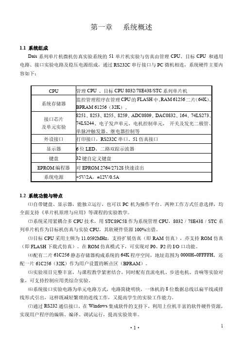
第一章系统概述1.1 系统组成Dais系列单片机微机仿真实验系统的51单片机实验与仿真由管理CPU、目标CPU 和通用电路、接口实验电路及稳压电源组成,通过RS232C串行接口与PC微机相连,系统硬件主要内容如下:CPU 管理CPU 、目标CPU 8032/78E438/STC系列单片机系统存储器监控管理程序在管理CPU的FLASH中、RAM 61256二片(64K)、BPRAM 61256(32K)。
接口芯片及单元实验8251、8253、8255、8259、ADC0809、DAC0832、164、74LS273、74LS244、电子发声单元,电机控制单元,开关及发光二极管、单脉冲触发器、继电器控制等外设接口打印接口,RS232C串口、51仿真接口显示器6位LED、二路双踪示波器键盘32键自定义键盘EPROM编程器对EPROM 2764/27128快速读出系统电源+5V/2A,±12V/0.5A1.2 系统功能与特点⑴自带键盘、显示器,能独立运行,也可以PC机为操作平台。
两种工作方式任意选择,均全面支持《单片机原理与应用》等课程的实验教学。
⑵系统采用紧耦合多CPU技术,用STC89C58作为系统管理CPU,8032 / 78E438 / STC系列单片机作为目标机仿真与实验CPU,其软硬件资源100%出借。
⑶目标CPU采用主频为11.0592MHz,支持扩展仿真(即RAM仿真),亦支持ROM仿真(即FLASH下载式仿真)。
在ROM仿真模式下,可实现对P0、P2的I/O口功能。
⑷配有二片61C256静态存储器构成系统的64K程序空间,地址范围为0000H~0FFFFH,还配一片61C256(32K)作为用户设置的断点区(BPRAM)。
⑸实验项目完整丰富,与课程教学紧密结合,同时配有直流电机、步进电机、音响等实验对象,可支持控制应用类综合实验。
⑹系统接口实验电路为单元电路方式,电路简捷明快,一体机的8位数据总线以扁平线或排线形式引出,这样既减轻繁琐的连线工作,又提高学生的实验工作能力。
横河PLC-FA-M3概述
FA-M3 主单元
顺控 CPU 模块
光纤 FA-总线 2 模块
电源 模块
顺控 CPU (最多3个槽位)) 辅助单元 1
系统配置
上级通信
- 通过以太网与工作站或个人电脑连接
工作站或个人电脑
以太网 FA-M3
- 通过个人电脑链接模块与图形显示控制面板连接
工作站或个人电脑
FA-M3
调制解调器模块
公共电话线
外形尺寸٠FA-M3 符合的标准......................................................................................................39
Yokogawa Electric Corporation
GS 34M6A01-01C © 版权所有 2006 年 1 月
通用技术规格٠电源规格........................................................................................ 5 性能规格 ................................................................................................................. 6 FA-M3 Value /FA-M3 Value II 的顺控 CPU 模块性能规格 ...........................9, 10 梯形图顺序基本指令/ ...........................................................................................11 梯形图顺序应用指令.............................................................................................12
U盘维修复活工具介绍

慧荣SM32x主控最新量产工具V1.17.42 H1029 (20081101发布) /read.php?tid=65117SM324BC+K9W SLC FLASH专用版量产工具(20081022发布)/read.php?tid=60187SM3251_321CC_DG_针对黑片的最新量产工具V1.17.40 (20081008发布)/read.php?tid=59116SM32X量产工具H0828版/read.php?tid=57092慧荣SM32x主控最新量产工具V1.17.38 H0821/read.php?tid=51044SM32X量产工具H0328汉化版/read.php?tid=30538SM32X量产工具H0229(V1.17.20汉化版)/read.php?tid=27371SMI SM32x H20080109量产修复工具简体中文汉化版/read.php?tid=272232008年首版SMI H0109量产工具及FLASH支持列表/read.php?tid=27218SM32x量产工具G2*******汉化版-每个字都是手工输入的,望支持/read.php?tid=25553SM32x量产工具G1219汉化版/read.php?tid-25553.htmlSM321&SM323 U盘量产修复工具下载,适用朗科U盘/read.php?tid=3970SMI32X主控U盘量产修复程序下载/read.php?tid=5811SM321最新版本1.7量产工具(支持多种芯片)/read.php?tid=15377最新惠荣SMI SM223 CF卡量产工具,支持SSD固态硬盘量产!/read.php?tid=52025群联Phison方案群联Phison UP10 UP12 UP13 UP14 u盘量产工具V1.06官方版本Phison PS2233 量产工具v1.03 破解版支持自定义VID PID【仅发数码之家】/read.php?tid=65779PS2233量产工具V1.03数码之家首发/read.php?tid=61127PS2232(UP13/UP14) MP TOOL V1.05.00新鲜版(目前最新)/read.php?tid=60779&fpage=3群联UP13/14(PS2232)最新量产工具放出(版本号奇怪,为1.0.20.3,不是1.96往后排)! /read.php?tid=60541Phison UP13/UP14/UP12量产工具V1.96/read.php?tid=31113PHISON UP12(PS2231) &UP10(PS2136)量产工具V1.89/read.php?tid-20398.html群联phison 2143-2134系列U盘量产格式化修复程序下载V1.28/read.php?tid=5806群联phison UP8-R 主控U盘量产格式化工具下载V2.0/read.php?tid=5800PHISON UP8-Y 专用量产工具V1.65/read.php?tid-18943.html群联UP10(PS2136)、UP11低格工具/read.php?tid=15433phison UP10主控U盘量产修复工具下载v1.78,感谢zhby9462提供/read.php?tid=6984群联Phison最新版量产工具V1.81 适用于PS2136(UP10)等主控/read.php?tid=15046群联Phison UP12 (PS2231)量产修复工具V1.85/read.php?tid-17925.htmlPNY U盘修复工具Pretest v1.11(群联)/read.php?tid=16858群联Phison UP10低格工具 1.30.0.0版下载/read.php?tid-23352.html群联Phison UP14(PS2232)主控u盘加密工具!/read.php?tid=60599群联Phsion UP10 ~14(PS2232)u盘主控最新加密工具V2.64中文版。
三菱编程软件(FB)
4 利用已存在的 FB 创建顺控程序
4-1 到 4-10
4.1 为 FB 创建工程 ......................................................................4 - 1 4.1.1 创建新工程 .....................................................................4 - 1 4.1.2 读取已存在的工程 ...............................................................8
1.1 什么是功能块(FB)? ..................................................................1 - 1 1.2 特点 ...............................................................................1 - 2 1.3 创建 FB 所用窗口的结构和名称 ........................................................1 - 2 1.4 使用 FB 之前您应该了解什么 ..........................................................1 - 5 1.5 规格 ...............................................................................1 - 5
3.12 修正 FB...........................................................................3 - 43 3.13 对顺控程序进行在线程序写入 .......................................................3 - 44
DSP入门教程
中国 DSP 网论坛:/bbs
2)版上发问 3)google 搜 4)再不济,找技术支持,碰运气了 3、如何看待 TI DSP 庞杂的技术文档 新手进行 DSP 开发学习之时,常常感觉技术文档太多,哪本都有用,哪本都想看,无从下 手。此时原则是只看入门必须的、只看和芯片相关的。根据经验,如下的资料必看不可: 1)讲述 DSP 的 CPU,memory,program memory addressing,data memory addressing 的资料 都需要看、外设资源的资料可以只看自己用到的部分; 2)C 和汇编的编程指南需要看 3)汇编指令和 C 语言的运行时间支持库、DSPLIB 等资料需要看其他的如:Applications Guide,Optimizing CC++ Compiler User's Guide,Assembly Language Tools User's Guide 等资 料留待入门之后再去看体会会更深一些。 4、如何高效开始 TI DSP 的硬件开发 1)根据应用领域选择 TI 推荐的 DSP 类型 2)参考选定的 DSP 之 EVM 板,DSK 等原理图,完成 DSP 最小系统的搭建(包括外扩内 存空间、电源复位系统、各控制信号管脚的连接、JTAG 口的连接等); 3)根据具体应用需要,选择外围电路的扩展,一般如语音、视频、控制等领域均有成熟的 电路可以从 TI 网站得到。外围电路与 DSP 的接口可参看 EVM 或 DSK,以及所选外围电路 芯片的典型接口设计原理图;最好外围电路芯片也选择 TI 的,这样的话不管硬件接口有现 成原理图、很多连 DSP 与其接口的基本控制源码都有。 4)地址译码、IO 扩展等用 CPLD 或者 FPGA 来做,将 DSP 的地址线、数据线、控制信号 线如 IS/PS/DS 等都引进去有利于调试 5、如何高效开始 TI DSP 的软件开发 如果你不是纯做算法,而是在一个目标版上进行开发,需要使用 DSP 的片上外设,需要控 制片外接口电路, 那么建议在写程序前先好好将这个目标版的电路设计搞清楚。 最重要的是 程序、 数据、 I/O 空间的译码。 不管是否纯做算法还是软硬结合, DSP 的 CPU,memory,program memory addressing, data mem.ory addressing 的资料都需要看. 1)看 CCS 的使用指南 2)明白 CMD 文件的编写
HT46R23资料

HT46R238-Bit OTP MicrocontrollerI 2C is a trademark of Philips Semiconductors.Rev.1.301August 17,2001General DescriptionThe device is an 8-bit high performance RISC-like microcontroller designed for multiple I/O product appli-cations.It is particularly suitable for use in products such as washing machine controllers and home appli-ances.A HALT feature is included to reduce power con-sumption.The program and option memories can be electrically programmed,making this microcontroller suitable for product development applications.Features·Operating voltage:f SYS =4MHz:3.3V~5.5V f SYS =8MHz:4.5V~5.5V·23bidirectional I/O lines (max.)·1interrupt input shared with an I/O line·16-bit programmable timer/event counter with overflowinterrupt and 7-stage prescaler·On-chip crystal and RC oscillator ·Watchdog Timer·4096´15program memory PROM ·192´8data memory RAM·Supports PFD for sound generation·HALT function and wake-up feature reduce powerconsumption·Up to 0.5m s instruction cycle with 8MHz system clockat V DD =5V·8-level subroutine nesting·8channels 10-bit resolution (9-bit accuracy)A/D con-verter·2-channel (6+2)/(7+1)-bit PWM output shared withtwo I/O lines·Bit manipulation instruction ·15-bit table read instruction ·63powerful instructions·All instructions in one or two machine cycles ·Low voltage reset function ·I 2C BUS (slave mode)·24/28-pin SKDIP/SOPpackageBlock DiagramPin AssignmentRev.1.302August 17,2001cPin DescriptionPin Name I/O ROM CodeOption Description PB0/AN0PB1/AN1PB2/AN2PB3/AN3 PB4/AN4 PB5/AN5 PB6/AN6 PB7/AN7I/O Pull-highBidirectional8-bit input/output port.Software instructions determine theCMOS output,Schmitt trigger input with or without pull-high resistor(deter-mined by pull-high option:port option)or A/D input.Once a PB line is selected as an A/D input(by using software control),theI/O function and pull-high resistor are disabled automatically.PA0~PA2 PA3/PFDPA4/TMR PA5/INT PA6/SDA PA7/SCL I/OPull-highWake-upPA3or PFDI/O or Serial BusBidirectional8-bit input/output port.Each bit can be configured as wake-upinput by ROM code option.Software instructions determine the CMOS out-put or Schmitt trigger input with or without pull-high resistor(determined bypull-high options:bit option).The PFD,TMR and INT are pin-shared withPA3,PA4and PA5,respectively.Once the I2C BUS function is used,the in-ternal registers related to PA6and PA7can not be used.VSS¾¾Negative power supply,ground.PC0~PC4I/O Pull-high Bidirectional5-bit input/output port.Software instructions determine the CMOS output,Schmitt trigger input with or without pull-high resistor(deter-mine by pull-high option:port option).PD0/PWM0 PD1/PWM1I/OPull-highI/O or PWMBidirectional2-bit input/output port.Software instructions determine theCMOS output,Schmitt trigger input with or without a pull-high resistor(de-termined by pull-high option:port option).The PWM0/PWM1output func-tion are pin-shared with PD0/PD1(dependent on PWM optios).RES I¾Schmitt trigger reset input.Active low. VDD¾¾Positive power supplyOSC1 OSC2IOCrystalor RCOSC1,OSC2are connected to an RC network or a Crystal(determined byROM code option)for the internal system clock.In the case of RC opera-tion,OSC2is the output terminal for1/4system clock.Absolute Maximum RatingsSupply Voltage...........................V SS-0.3V to V SS+5.5V Storage Temperature............................-50°C to125°C Input Voltage..............................V SS-0.3V to V DD+0.3V Operating Temperature...........................-40°C to85°CNote:These are stress ratings only.Stresses exceeding the range specified under²Absolute Maximum Ratings²may cause substantial damage to the device.Functional operation of this device at other conditions beyond those listed in the specification is not implied and prolonged exposure to extreme conditions may affect device reliabil-ity.Rev.1.303August17,2001Symbol ParameterTest ConditionsMin.Typ.Max.Unit V DD ConditionsV DD1Operating Voltage¾f SYS=4MHz 3.3¾ 5.5V V DD2Operating Voltage¾f SYS=8MHz 4.5¾ 5.5VI DD1Operating Current(Crystal OSC)3.3V No load,fSYS=4MHzADC disable¾ 1.33mA 5V¾ 3.35mAI DD2Operating Current(RC OSC)3.3V No load,fSYS=4MHzADC disable¾ 1.33mA 5V¾ 3.35mAI DD3Operating Current5V No load,fsys=8MHzADC disable¾48mAI ADC Only ADC Enable,Others Disable 3.3VNo load¾12mA 5V¾24mAI STB1Standby Current(WDT Enabled)3.3VNo load,system HALT¾¾5m A 5V¾¾10m AI STB2Standby Current(WDT Disabled)3.3VNo load,system HALT¾¾1m A 5V¾¾2m AV AD A/D Input Voltage¾¾0¾V DD VV IL1Input Low Voltage for I/O Ports,TMR and INT 3.3V¾0¾0.3V DD V 5V¾0¾0.3V DD VV IH1Input High Voltage for I/O Ports,TMR and INT 3.3V¾0.7V DD¾V DD V 5V¾0.7V DD¾V DD VV IL2Input Low Voltage(RES)3.3V¾0¾0.4V DD V 5V¾0¾0.4V DD VV IH2Input High Voltage(RES)3.3V¾0.9V DD¾V DD V 5V¾0.9V DD¾V DD VV LVR Low Voltage Reset¾¾ 2.73 3.3VI OL I/O Port Sink Current 3.3V V OL=0.1V DD48¾mA 5V V OL=0.1V DD1020¾mAI OH I/O Port Source Current 3.3V V OH=0.9V DD-2-4¾mA 5V V OH=0.9V DD-5-10¾mAR PH Pull-high Resistance 3.3V¾406080k W 5V¾103050k WE AD A/D Conversion Error5V¾¾±0.5±1LSB Rev.1.304August17,2001Symbol ParameterTest ConditionsMin.Typ.Max.Unit V DD Conditionsf SYS1System Clock(Crystal OSC)3.3V¾400¾4000kHz 5V¾400¾8000kHzf SYS2System Clock(RC OSC)3.3V¾400¾4000kHz 5V¾400¾8000kHzf TIMER Timer I/P Frequency(TMR)3.3V¾0¾4000kHz 5V¾0¾8000kHzt AD A/D Clock Period5V¾1¾¾m s t ADC A/D Conversion Time¾¾¾76¾t ADt WDTOSC Watchdog Oscillator 3.3V¾4386168m s 5V¾3672144m st RES External Reset Low Pulse Width¾¾1¾¾m st SST System Start-up Timer Period¾Power-up,reset orwake-up from HALT¾1024¾*t SYS t INT Interrupt Pulse Width¾¾1¾¾m st HBUS I2C BUS Clock Period¾Connect to externalpull-high resistor2k W64¾¾*t SYS Note:*t SYS=1/f SYSRev.1.305August17,2001Functional DescriptionExecution flowThe system clock for the microcontroller is derived from either a crystal or an RC oscillator.The system clock is internally divided into four non-overlapping clocks.One instruction cycle consists of four system clock cycles. Instruction fetching and execution are pipelined in such a way that a fetch takes an instruction cycle while de-coding and execution takes the next instruction cycle. However,the pipelining scheme causes each instruc-tion to effectively execute in a cycle.If an instruction changes the program counter,two cycles are required to complete the instruction.Program counter-PCThe program counter(PC)controls the sequence in which the instructions stored in program PROM are exe-cuted and its contents specify full range of program memory.After accessing a program memory word to fetch an in-struction code,the contents of the program counter are in-cremented by one.The program counter then points to the memory word containing the next instruction code. When executing a jump instruction,conditional skip ex-ecution,loading PCL register,subroutine call,initial re-set,internal interrupt,external interrupt or return from subroutine,the PC manipulates the program transfer by loading the address corresponding to each instruction. The conditional skip is activated by instructions.Once the condition is met,the next instruction,fetched during the current instruction execution,is discarded and a dummy cycle replaces it to get the proper instruction. Otherwise proceed with the next instruction.The lower byte of the program counter(PCL)is a read-able and writeable register(06H).Moving data into the PCL performs a short jump.The destination will be within256locations.When a control transfer takes place,an additional dummy cycle is required.FcFcFcExecution flowModeProgram Counter*11*10*9*8*7*6*5*4*3*2*1*0Initial Reset000000000000 External Interrupt000000000100 Timer/Event Counter Overflow000000001000 A/D Converter Interrupt000000001100 I2C BUS Interrupt000000010000 Skip PC+2Loading PCL*11*10*9*8@7@6@5@4@3@2@1@0 Jump,Call Branch#11#10#9#8#7#6#5#4#3#2#1#0 Return from Subroutine S11S10S9S8S7S6S5S4S3S2S1S0Program counterNote:*11~*0:Program counter bits S11~S0:Stack register bits#11~#0:Instruction code bits@7~@0:PCL bitsRev.1.306August17,2001Program memory-PROMThe program memory is used to store the program in-structions which are to be executed.It also contains data,table,and interrupt entries,and is organized into 4096´15bits,addressed by the program counter and ta-ble pointer.Certain locations in the program memory are reserved for special usage:·Location000HThis area is reserved for program initialization.After chip reset,the program always begins execution at lo-cation000H.·Location004HThis area is reserved for the external interrupt service program.If the INT input pin is activated,the interrupt is enabled and the stack is not full,the program begins execution at location004H.·Location008HThis area is reserved for the timer/event counter inter-rupt service program.If a timer interrupt results from a timer/event counter overflow,and if the interrupt is en-abled and the stack is not full,the program begins exe-cution at location008H.·Location00CHThis area is reserved for the A/D converter interrupt service program.If an A/D converter interrupt results from an end of A/D conversion,and if the interrupt is enabled and the stack is not full,the program begins execution at location00CH.·Location010HThis area is reserved for the I2C BUS interrupt service program.If the I2C BUS interrupt resulting from a slave address is match or completed one byte of data transfer,and if the interrupt is enable and the stack is not full,the program begins execution at location 010H.·Table locationAny location in the PROM space can be used as look-up tables.The instructions²TABRDC[m]²(the current page,1page=256words)and²TABRDL[m]²(the last page)transfer the contents of the lower-order byte to the specified data memory,and the higher-order byte to TBLH(08H).Only the destination of the lower-order byte in the table is well-defined,the other bits of the table word are transferred to the lower portion of TBLH,and the remaining1bit is read as²0². The Table Higher-order byte register(TBLH)is read only.The table pointer(TBLP)is a read/write register (07H),which indicates the table location.Before ac-cessing the table,the location must be placed in TBLP.The TBLH is read only and cannot be restored. If the main routine and the ISR(Interrupt Service Rou-tine)both employ the table read instruction,the con-tents of the TBLH in the main routine are likely to be changed by the table read instruction used in the ISR. Errors can occur.In other words,using the table read instruction in the main routine and the ISR simulta-neously should be avoided.However,if the table read instruction has to be applied in both the main routine and the ISR,the interrupt is supposed to be disabled prior to the table read instruction.It will not be enabled until the TBLH has been backed up.All table related instructions require two cycles to complete the opera-tion.These areas may function as normal program memory depending upon the requirements.Program memoryInstructionTable Location*11*10*9*8*7*6*5*4*3*2*1*0TABRDC[m]P11P10P9P8@7@6@5@4@3@2@1@0 TABRDL[m]1111@7@6@5@4@3@2@1@0Table locationNote:*11~*0:Table location bits P11~P8:Current program counter bits @7~@0:Table pointer bitsRev.1.307August17,2001Stack register-STACKThis is a special part of the memory which is used to save the contents of the program counter(PC)only.The stack is organized into8levels and is neither part of the data nor part of the program space,and is neither read-able nor writeable.The activated level is indexed by the stack pointer(SP)and is neither readable nor writeable. At a subroutine call or interrupt acknowledgment,the contents of the program counter are pushed onto the stack.At the end of a subroutine or an interrupt routine, signaled by a return instruction(RET or RETI),the pro-gram counter is restored to its previous value from the stack.After a chip reset,the SP will point to the top of the stack.If the stack is full and a non-masked interrupt takes place,the interrupt request flag will be recorded but the acknowledgment will be inhibited.When the stack pointer is decremented(by RET or RETI),the interrupt will be serviced.This feature prevents stack overflow al-lowing the programmer to use the structure more easily. In a similar case,if the stack is full and a²CALL²is sub-sequently executed,stack overflow occurs and the first entry will be lost(only the most recent8return ad-dresses are stored).Data memory-RAMThe data memory is designed with224´8bits.The data memory is divided into two functional groups:spe-cial function registers and general purpose data mem-ory(192´8).Most are read/write,but some are read only.The special function registers include the indirect ad-dressing registers(00H;02H),timer/event counter higher-order byte register(TMRH;0CH),timer/event counter low-order byte register(TMRL;0DH), timer/event counter control register(TMRC;0EH),pro-gram counter lower-order byte register(PCL;06H), memory pointer registers(MP0;01H,MP1;03H),accu-mulator(ACC;05H),table pointer(TBLP;07H),table higher-order byte register(TBLH;08H),status register (STATUS;0AH),interrupt control register(INTC0; 0BH),PWM data register(PWM0;1AH,PWM1;1BH), the I2C BUS slave address register(HADR;20H),the I2C BUS control register(HCR;21H),the I2C BUS status regis-ter(HSR;22H),the I2C BUS data register(HDR;23H),the A/D result lower-order byte register(ADRL;24H),the A/D result higher-order byte register(ADRH;25H),the A/D con-trol register(ADCR;26H),the A/D clock setting register (ACSR;27H),I/O registers(PA;12H,PB;14H,PC;16H, PD;18H)and I/O control registers(PAC;13H,PBC;15H, PCC;17H,PDC;19H).The remaining space before the 40H is reserved for future expanded usage and reading these locations will get²00H².The general purpose data memory,addressed from40H to FFH,is used for data and control information under instruction commands.All of the data memory areas can handle arithmetic, logic,increment,decrement and rotate operations di-rectly.Except for some dedicated bits,each bit in the data memory can be set and reset by²SET[m].i²and ²CLR[m].i².They are also indirectly accessible through memory pointer registers(MP0;01H/MP1;03H).RAM mappingRev.1.308August17,2001Indirect addressing registerLocation00H and02H are indirect addressing registers that are not physically implemented.Any read/write op-eration of[00H]or[02H]will access data memory pointed to by MP0[01H]or MP1[03H]respectively. Reading location00H or02H itself indirectly will return the result00H.Writing indirectly result in no operation. The memory pointer registers(MP0and MP1are8-bit registers).AccumulatorThe accumulator is closely related to ALU operations.It is also mapped to location05H of the data memory and can carry out immediate data operations.The data movement between two data memory locations must pass through the accumulator.Arithmetic and logic unit-ALUThis circuit performs8-bit arithmetic and logic operations. The ALU provides the following functions:·Arithmetic operations(ADD,ADC,SUB,SBC,DAA)·Logic operations(AND,OR,XOR,CPL)·Rotation(RL,RR,RLC,RRC)·Increment and Decrement(INC,DEC)·Branch decision(SZ,SNZ,SIZ,SDZ....)The ALU not only saves the results of a data operation but also changes the status register.Status register-STATUSThis8-bit register(0AH)contains the zero flag(Z),carry flag(C),auxiliary carry flag(AC),overflow flag(OV), power down flag(PD),and watchdog time-out flag(TO). It also records the status information and controls the operation sequence.With the exception of the TO and PD flags,bits in the status register can be altered by instructions like most other registers.Any data written into the status register will not change the TO or PD flag.In addition operations related to the status register may give dif-ferent results from those intended.The TO flag can be affected only by system power-up,a WDT time-out or executing the²CLR WDT²or²HALT²in-struction.The PD flag can be affected only by exe-cuting the²HALT²or²CLR WDT²instruction or a system power-up.The Z,OV,AC and C flags generally reflect the status of the latest operations.In addition,on entering the interrupt sequence or exe-cuting the subroutine call,the status register will not be pushed onto the stack automatically.If the contents of the status are important and if the subroutine can cor-rupt the status register,precautions must be taken to save it properly.InterruptThe device provides an external interrupt,an internal timer/event counter interrupt,the A/D converter interrupt and the I2C BUS interrupts.The interrupt control register 0(INTC0;0BH)and interrupt control register1 (INTC1;1EH)contains the interrupt control bits to set the enable/disable and the interrupt request flags.Once an interrupt subroutine is serviced,all the other in-terrupts will be blocked(by clearing the EMI bit).This scheme may prevent any further interrupt nesting.Other interrupt requests may happen during this interval but only the interrupt request flag is recorded.If a certain in-terrupt requires servicing within the service routine,the EMI bit and the corresponding bit of INTC0and INTC1 may be set to allow interrupt nesting.If the stack is full, the interrupt request will not be acknowledged,even if the related interrupt is enabled,until the SP is decremented. If immediate service is desired,the stack must be pre-vented from becoming full.All these kinds of interrupts have a wake-up capability. As an interrupt is serviced,a control transfer occurs by pushing the program counter onto the stack,followed byLabels Bits FunctionC0C is set if the operation results in a carry during an addition operation or if a borrow does not take place during a subtraction operation;otherwise C is cleared.C is also affected by a rotate through carry instruction.AC1AC is set if the operation results in a carry out of the low nibbles in addition or no borrow from the high nibble into the low nibble in subtraction;otherwise AC is cleared.Z2Z is set if the result of an arithmetic or logic operation is zero;otherwise Z is cleared.OV3OV is set if the operation results in a carry into the highest-order bit but not a carry out of the highest-order bit,or vice versa;otherwise OV is cleared.PD4PD is cleared by system power-up or executing the²CLR WDT²instruction.PD is set by exe-cuting the²HALT²instruction.TO5TO is cleared by system power-up or executing the²CLR WDT²or²HALT²instruction.TO is set by a WDT time-out.¾6,7Unused bit,read as²0²Status registerRev.1.309August17,2001a branch to a subroutine at specified location in the pro-gram memory.Only the program counter is pushed onto the stack.If the contents of the register or status register (STATUS)are altered by the interrupt service program which corrupts the desired control sequence,the con-tents should be saved in advance.External interrupts are triggered by a high to low transi-tion of and the related interrupt request flag(EIF;bit 4of INTC0)will be set.When the interrupt is enabled, the stack is not full and the external interrupt is active,a subroutine call to location04H will occur.The interrupt request flag(EIF)and EMI bits will be cleared to disable other interrupts.The internal timer/event counter interrupt is initialized by setting the timer/event counter interrupt request flag (TF;bit5of INTC0),caused by a timer overflow.When the interrupt is enabled,the stack is not full and the TF bit is set,a subroutine call to location08H will occur.The related interrupt request flag(TF)will be reset and the EMI bit cleared to disable further interrupts.The A/D converter interrupt is initialized by setting the A/D converter request flag(ADF;bit6of INTC0), caused by an end of A/D conversion.When the interrupt is enabled,the stack is not full and the ADF is set,a sub-routine call to location0CH will occur.The related inter-rupt request flag(ADF)will be reset and the EMI bit cleared to disable further interrupts.Register Bit bel FunctionINTC0 (0BH)0EMIControls the master(global)interrupt(1=enabled;0=disabled)1EEIControls the external interrupt(1=enabled;0=disabled)2ETIControls the timer/eventcounter interrupt(1=enabled;0=disabled)3EADIControls the A/D converterinterrupt(1=enabled;0=disabled)4EIFExternal interrupt request flag(1=active;0=inactive)5TFInternal timer/event counterrequest flag(1=active;0=inactive)6ADFA/D converter request flag(1=active;0=inactive)7¾Unused bit,read as²0²INTC0registerThe I2C BUS interrupt is initialized by setting the I2C BUS interrupt request flag(HIF;bit4of INTC1),caused by a slave address match(HAAS=²1²)or one byte of data transfer is completed.When the interrupt is enabled,the stack is not full and the HIF bit is set,a subroutine call to location10H will occur.The related interrupt request flag (HIF)will be reset and the EMI bit cleared to disable further interrupts.During the execution of an interrupt subroutine,other in-terrupt acknowledgments are held until the²RETI²in-struction is executed or the EMI bit and the related interrupt control bit are set to1(of course,if the stack is not full).T o return from the interrupt subroutine,²RET²or ²RETI²may be invoked.RETI will set the EMI bit to en-able an interrupt service,but RET will not. Interrupts,occurring in the interval between the rising edges of two consecutive T2pulses,will be serviced on the latter of the two T2pulses,if the corresponding inter-rupts are enabled.In the case of simultaneous requests the following table shows the priority that is applied. These can be masked by resetting the EMI bit.No.Interrupt Source Priority Vectora External Interrupt104Hb Timer/event Counter Overflow208Hc A/D Converter Interrupt30CHd I2C BUS Interrupt410H The timer/event counter interrupt request flag(TF),ex-ternal interrupt request flag(EIF),A/D converter request flag(ADF),the I2C BUS interrupt request flag(HIF),en-able timer/event counter bit(ETI),enable external inter-rupt bit(EEI),enable A/D converter interrupt bit(EADI), enable I2C BUS interrupt bit(EHI)and enable master in-terrupt bit(EMI)constitute an interrupt control register0 (INTC0)and an interrupt control register1(INTC1) which are located at0BH and1EH in the data memory. EMI,EEI,ETI,EADI,EHI are used to control the en-abling/disabling of interrupts.These bits prevent the re-quested interrupt from being serviced.Once the interrupt request flags(TF,EIF,ADF,HIF)are set,they will remain in the INTC0and INTC1register until the in-terrupts are serviced or cleared by a software instruc-tion.Register Bit bel FunctionINTC1(1EH)0EHIControls the I2C BUS inter-rupt(1=enabled;0=disabled)1¾Unused bit,read as²0²2¾Unused bit,read as²0²3¾Unused bit,read as²0²4HIFI2C BUS interrupt requestflag(1=active;0=inactive)5¾Unused bit,read as²0²6¾Unused bit,read as²0²7¾Unused bit,read as²0²INTC1registerRev.1.3010August17,2001It is recommended that a program does not use the²CALL subroutine²within the interrupt subroutine.In-terrupts often occur in an unpredictable manner or need to be serviced immediately in some applications. If only one stack is left and enabling the interrupt is not well controlled,the original control sequence will be dam-aged once the²CALL²operates in the interrupt subrou-tine.Oscillator configurationThere are two oscillator circuits in the microcontroller. Both are designed for system clocks,namely the RC os-cillator and the Crystal oscillator,which are determined by the ROM code option.No matter what oscillator type is selected,the signal provides the system clock.The HALT mode stops the system oscillator and ignores anexternal signal to conserve power.If an RC oscillator is used,an external resistor between OSC1and VSS is required and the resistance must range from30k W to750k W.The system clock,divided by4,is available on OSC2,which can be used to syn-chronize external logic.The RC oscillator provides the most cost effective solution.However,the frequency of oscillation may vary with VDD,temperatures and the chip itself due to process variations.It is,therefore,not suitable for timing sensitive operations where an accu-rate oscillator frequency is desired.If the Crystal oscillator is used,a crystal across OSC1 and OSC2is needed to provide the feedback and phase shift required for the oscillator,and no other external components are required.Instead of a crystal,a resona-tor can also be connected between OSC1and OSC2to get a frequency reference,but two external capacitors in OSC1and OSC2are required(If the oscillating fre-quency is less than1MHz).The WDT oscillator is a free running on-chip RC oscillator, and no external components are required.Even if the sys-tem enters the power down mode,the system clock is stopped,but the WDT oscillator still works with a period of approximately72m s/5V.The WDT oscillator can be dis-abled by ROM code option to conserve power. Watchdog Timer-WDTThe clock source of the WDT is implemented by an dedi-cated RC oscillator(WDT oscillator)or instruction clock (system clock divided by4)decided by ROM code op-tions.This timer is designed to prevent a software mal-function or sequence jumping to an unknown location with unpredictable results.The watchdog timer can be disabled by a ROM code option.If the watchdog timer is disabled,all the executions related to the WDT result in no operation.Once an internal WDT oscillator(RC oscillator with pe-riod72m s normally)is selected,it is divided by212~215 (by ROM code option to get the WDT time-out period). The minimum period of WDT time-out period is about 300ms~600ms.This time-out period may vary with tem-perature,VDD and process variations.By selection the WDT ROM code option,longer time-out periods can be realized.If the WDT time-out is selected215,the maxi-mum time-out period is divided by215~216about 2.3s~4.7s.If the WDT oscillator is disabled,the WDT clock may still cone from the instruction clock and operate in the same manner except that in the halt state the WDT may stop counting and lose its protecting purpose.In this situation the logic can only be restarted by external logic.If the device operates in a noisy environment,using the on-chip RC oscillator(WDT OSC)is strongly recom-mended,since the HALT will stop the system clock. The WDT overflow under normal operation will initialize ²chip reset²and set the status bit TO.Whereas in the halt mode,the overflow will initialize a²warm reset²only the PC and SP are reset to zero.T o clear the contents of WDT, three methods are adopted;external reset(a low level to RES),software instructions,or a HALT instruction.The software instructions include CLR WDT and the other set-c cSystem oscillatorWatchdog TimerRev.1.3011August17,2001。
MBR分区表
MBR分区表构成MBR分区表以80为起始,以55AA为结束,共64个字节,分为4个分区表,一个可启动分区和三个不可启动分区。
其结构如下:分区表一:第1个字节80(HEX) *可启动分区第2~4字节01/01/00(HEX)*开始磁头/开始扇区/开始柱面换算一下,二进制表示就是。
0000 0001/00000001/0000 0000(BIN)*开始磁头/开始扇区/开始柱面以下将使用16进制表示,不再换算成二进制!第五个字节0C *分区类型FAT32 NTFS为07,可自己变更第6~8字节FE/FF/FF *结束磁头/结束扇区/结束柱面第9~12字节00 00 00 3F *分区前的隐藏扇区63个隐藏扇区,此设计使0磁道使用0扇区,而1到62扇区不使用,减少读取,以此保护分区表,个人认为是个很不错的设计,不过很少有人知道这个。
第13~16字节5B 24 40 01 *分区大小20980827个扇区当然好要算上分区表的63个扇区一共20980889个扇区合10GB 公式为20980889*512/(1024^3)=10GB------------------------------------------------------我是一条分割线-----------------------------------------------分区表二:第17个字节00:不可启动分区第18~20字节开始磁头/开始扇区/开始柱面第21字节0F *分区类型为扩展分区第22~24字节结束磁头/结束扇区/结束柱面第25~28字节分区前的隐藏扇区第29~32字节分区大小分区表三,分区表四,以此类推,不再解释。
至于分区表的修改WinHex(DISKEDIT DOS下)是个不错的软件,了解了这些,就可以自己重建分区表了。
另:MBR是主分区表,误操作使MBR损坏时,DBR或者DBR备份应该没损坏,我们可以通过搜索55AA来获得DBR信息(往前找就行了),来寻找DBR从而了解更多信息(主要是分区大小和开始结束的扇区,磁头,柱头),来帮助我们重建分区表。
罗托克电动头中文说明书
IQ10至IQ35
B型非推力底座
卸下底盘的四个螺栓,确保底盘的安全,卸下底盘。
此时可看到驱动轴套和卡簧。
B3和B4型的拆卸:
(参见图7a)
用外卡簧钳涨开卡簧,同时向外拉驱动轴套。驱动轴套将从
执行器中心套筒上脱开,但卡簧仍留在轴套的槽中。
图7a
B3和B4型的重新组装
润滑驱动轴套和卡簧。将卡簧装入驱动轴套的槽中,将驱动轴套送入执行器中心套筒底部,对准键和槽。
提升1
侧面安装
非提升杆式阀门-11
顶部安装
手轮密封11
IQM调节型执行器12
IQML线性推力装置12
IQML线性行程的调整12
6接线14
地线的连接14
端子箱盖的拆卸14
电缆入口14
端子的接线15
端子箱盖的复位15
7设定16
设定程序16
设定器17
进入设定程序18
如果需要进一步有关RotorkIQ系列执行器的资料和指南,我们将根据需要提供。
如果执行器不能立即安装,则应将它保存在一个干燥的地方,直到准备接线。
如果执行器已安装好,但还没有接线,那么建议您将电缆入口的塑料塞换成缠有聚四氟乙烯的密封金属塞。
如无意外,Rotork产品的双密封结构能很好地保护内部的电气元件。
图15上紧止挡圈的定位螺栓
IQ40至IQ95
B型非推力底座
B1型
输出轴的孔和键均符合ISO 5210标准。驱动轴套无需加工。
B3和B4型
此两种驱动轴套可根据顶部带帽的螺栓来鉴别。
B3在提供时已按ISO5210标准预加工。
B4在提供时为实心,需按阀门或齿轮箱的驱动轴进行加工。
单片机校园网资料
{2013级}土木工程系MCS-51单片机上机实验安排专页最新提供:实验人员分组名单(2015.10.28), 电子版实验报告样本,教材课后习题答案(PDF格式)(机房机器截图方法:按“Print Screen”键,屏幕内容会放入系统剪切板,然后在Word中用Ctrl+V贴过来,选中图片,点击图片工具栏上的“裁剪”按钮,然后调整图片的边缘到合适位置即可,四面都能调整。
如果不出“图片”工具栏,点“视图-》工具栏-》图片”,挑上勾就能出来了。
保存的时候记得压缩一下图片,不保存裁掉的部分,能省些空间,具体操作方法是在保存对话框的右上角点“工具”,然后...)实验地点:软件部分(9-12周)在实验楼机房3楼ABC区,硬件部分(13-16周)在实验楼5楼机房。
实验时间:交通C131/2/3周日第1大节,土木C134/5和交运C131周日第2大节,给排水C131/2和交运C132周日第3大节。
本课上机须知(要点:实验时不要做与实验无关的事情!)本课实验用软件:(工具软件:PDF阅读器)伟福6000绿色版(WAVE6000使用说明.PDF)KEIL C51 V3.0, KEI L最新版(V4)(KEIL软件安装使用说明)硬件仿真器Proteus7.4版,7.12完美破解版 (Proteus软件安装步骤) (Keil 与proteus完美结合教程.pdf)相关资料:软件实验源程序:点此下载(使用方法:用KEIL软件的工程菜单下的“打开工程...”功能,寻找对应的uv2文件打开)实验书内容节选整体压缩包(手机翻拍,效果较差,但能看清是什么字。
适用内容为第1章、第2章和第4章的部分内容)封面,封底,前言,目录1,目录2第一章单片机集成开发环境(1,2,3,4,5,6,7,8,9,10,11,12,13,14,15,16,17)第2章 Proteus的单片机系统软件仿真,第4章单片机基础实验最新增补:2015.10.31翻拍的部分实验书内容,较上面的效果好些(多图杀猫,谨慎下载)。
STC89C51RC-RD单片机使用说明
宏晶科技:www.MCU-Memory.com Mobile:13922805190(姚永平) Tel:0755-82948409 Fax: 0755-82944243
STC89C51RC / RD+ 系列单片机 管脚图
WR/P3.6 P1.4 RD/P3.7 P1.3
R C / R D + 系列为真正的看门狗,缺省为关闭(冷启动),启动后无法关闭,可放心省去外部看门狗。
内部 Flash 擦写次数为 100,000 次以上,STC89C51RC/RD+ 系列单片机出厂时就已完全加密,无法解密。
用户程序是用 ISP/IAP 机制写入,一边校验一边写,无读出命令,彻底无法解密。DIP-40,PLCC-44,
STC89C51RC, STC89C52RC, STC89C53RC,
STC89LE51RC STC89LE52RC STC89LE53RC
STC89C54RD+, STC89LE54RD+ STC89C58RD+, STC89LE58RD+ STC89C516RD+, STC89LE516RD+
STC89LE516AD, STC89LE58AD STC89LE54AD, STC89LE52AD
PQFP-44 三种封装(PLCC、QFP 有 P4 口),RC/RD+ 系列单片机 P4 口地址为 E8H,并有 2 个附加外部中断,
P4.2/INT3,P4.3/INT2。STC89LE516AD/X2 系列单片机 P4 口地址为 C0H,无附加外部中断。 宏晶科技:专业单片机 / 存储器供应商 www.MCU-Memory.com STC 增强型 8051 单片机中文指南(RC/RD+ 系列) 2
32K 1280 √ √ √ √ √ √ 8K+ 2 1ch+ 8 4 3 W78E58 P89C58 AT89C51RC
- 1、下载文档前请自行甄别文档内容的完整性,平台不提供额外的编辑、内容补充、找答案等附加服务。
- 2、"仅部分预览"的文档,不可在线预览部分如存在完整性等问题,可反馈申请退款(可完整预览的文档不适用该条件!)。
- 3、如文档侵犯您的权益,请联系客服反馈,我们会尽快为您处理(人工客服工作时间:9:00-18:30)。
HANGZHOU KAWAI ELECTRIC CO., LTD.
MSP0706
版次: B版
编制王树明日期:2005年04月25日
审核胡光驰日期: 2005年04月25日
批准陈苹日期: 2005年04月29日
分发号
2005-04-30发布 2005-04-30实施
管理管理体系程序文件文件编号MSP0706
标题能、资源管理程序页次 1/5 修改次/版次 0/B
1. 目的
加强能、资源的管理,最大限度地提高能资源的有效利用率。
2. 适用范围
公司原材料、辅助材料、水、电等能资源的使用及其相关活动。
3. 职责
3.1 财务部负责确定产品单耗,主管材料消耗、废品损失的考核和管理。
3.2 工程部主管用水、用电的分析、控制及考核管理。
3.3 仓库负责原材料、辅助材料的贮存、发放的控制管理。
3.4各相关部门负责本部门原材料、辅助材料、水、电等能资源的消耗控制和管理,制定改进措施,降低损耗,节约能资源。
4. 工作程序
4.1原材料的控制
4.1.1体系管理室负责编制并监督运行《定额领料管理规定》。
4.1.2财务部编制《产品单耗表》,生产计划员编制《生产计划表》,通过网络传递给技术部、财务部、采购计划、仓库等部门,并下发书面通知给各相关制造部门。
4.1.3仓库根据《生产计划表》和《产品单耗表》,在网上编制《材料领用计划表》。
4.1.4制造部门根据《生产计划表》,填写相应批号产品的《材料领用单》或《管材领用清单》(热威管材),新批号开始领用时,部门主管
应核实签字确认。
《材料领用单》和《管材领用清单》一式三联,领用
管理体系程序文件文件编号MSP0706
标题能、资源管理程序页次 2/5 修改次/版次 0/B
部门一联,仓库两联,一联入库记帐,一联领用计划核对。
4.1.5仓库将《材料领用单》、《管材领用清单》与《材料领用计划表》核对无误后,签名并核销材料领用计划。
4.1.6仓库物管员根据核对后的《材料领用单》进行发货,并在“材料卡”上做好出库记录。
4.1.7过程中发现材料不良或产生了废品,制造部门要及时进行鉴定,并开具《不良品退库通知单》和《废品入库单》,不良品材料和废品经检验确认后送交仓库,仓库物管员核对后签收。
4.1.8因材料不良需补数时,由采购通知供应商补数,制造部门开具红字《材料领用单》冲帐,开具蓝字《材料领用单》进行补领。
因废品需补数时,由各制造部门填写《材料补数申请单》,交采购计划核准签字。
指标内补数由部门主管确认、部门经理审批,超指标补数由部门经理确认、制造总监和总经理(或其授权人)审批。
《材料补数申请单》按需要发至各有关部门,各部门配合做好相应的补数工作。
4.1.9仓库根据《生产计划表》和《材料补数申请单》,编制补数《材料领用计划表》。
4.1.10领料员根据《材料补数申请单》,填写相应补数产品的《材料补数领用单》或《管材领用清单》。
4.1.11 仓库严格按计划发料、凡计划外的补数材料一律按材料补数规定发放。
4.1.12每个生产批号完成后,制造部门要及时清理剩余的成品、半成品
管理体系程序文件文件编号MSP0706
页次 3/5
标题能、资源管理程序
及零配件,并办理入库手续。
4.1.13仓库记帐员每月对原材料领用、消耗情况进行统计、汇总,并将统计结果在网络上传递给有关部门。
4.1.14财务部根据原材料领用、消耗的统计和过程抽查核对结果,修正《产品单耗表》,并进行成本管理考核。
4.2辅助材料的控制
4.2.1技术部根据工艺需要和生产实际情况,制定清洗用化学危险品用量消耗定额,使用部门按定额领用。
确实需要增加时,使用部门提出申请、说明原因,由各部门经理审批。
4.2.2各部门开《领料单》到仓库领用油料等辅助材料,《领料单》一式三联,一联留底,两联仓库。
无库存时由仓库填写《采购单》报采购,其他辅助材料由领用部门向仓库提出领用申请,仓管员填写《采购单》,经申请部门经理批准后进行采购,办公用品、印刷用品、劳保用品等需经人事副总批准。
4.2.3各使用部门必须严格控制油料等辅助材料消耗,并按有关限额管理规定领用。
4.2.4财务部根据油料等辅助材料领用、消耗的情况进行成本管理考核。
4.3水的控制
4.3.1安全管理室按目标和指标及有关管理方案要求,督促责任部门执行相应的节水管理办法和具体措施。
安全管理室对各区域的用水量下达定额并进行月度消耗统计分析,分析结果记录在《用水统计分析表》上。
管理体系程序文件文件编号MSP0706
页次 4/5
标题能、资源管理程序
4.3.2安全管理室每月对各区域用水量进行平衡分析时,发现异常情况按《纠正/预防和改进程序》及时采取相应的措施。
4.3.3各区域的管理人员要监督员工用水后及时关紧阀门,形成节约用水的良好风气,避免不必要的浪费。
4.3.4水管和水阀门出现故障,各部门要及时通知维修部门修理和更换。
4.4电的控制
4.4.1工程部按目标和指标及有关管理方案要求,督促责任部门执行相应的节电管理办法和具体措施。
工程部对各区域的用电量下达定额并进行月度消耗统计分析,分析结果记录在《用电统计分析表》上。
4.4.2工程部对各区域用电量进行平衡分析时,发现异常情况按《纠正/预防和改进程序》及时采取相应的措施。
4.4.3各部门按具体方案要求落实节电措施,确保目标与指标的实现。
4.4.4对于各部门耗电量较大的设备,设备管理室应制定《设备维护保养计划》,定期对设备进行维护保养,加强检修,杜绝设备非正常运转。
4.4.5各部门内的照明灯应做到“人离灯灭”。
所有的空调使用应严格按设备管理室的有关管理规定执行。
4.4.6新安装的照明灯,应尽可能地采用“节能灯”。
4.4.7安全管理室应对用电情况进行检查,对各部门用电中存在的问题,按《纠正/预防和改进程序》执行。
4.5能、资源的再利用按《水、气、声及固废控制程序》执行。
4.6本程序所形成和涉及的记录按《记录控制程序》执行。
管理体系程序文件文件编号MSP0706
页次 5/5
标题能、资源管理程序
5. 相关/支持性文件
MSP0401《管理方案控制程序》
MSP0806《纠正/预防和改进程序》
MSP0405《记录控制程序》
MSP0705《水、气、声及固废控制程序》 MSC0708-5《定额领料管理规定》
6. 记录
MSR0706-5《产品单耗表》
MSR0706-1《材料领用单》
MSR0706-1a《材料补数领用单》
MSR0706-1b《管材领用清单》
MSR0706-2《材料领用计划表》
MSR0706-3《用水统计分析表》
MSR0706-4《用电统计分析表》
MSR0701-6《生产计划表》
MSR0703-1《采购单》
MSR0704-4《设备维护保养计划》
MSR0704-7《材料补数申请单》
MSR0804-3《废品入库单》
MSR0804-5《不良品退库通知单》
《领料单》。