A High Resolution, Low Offset And High Speed Comparator
LF353 PDF
Industrial Temperature Range (– 25°C to +85°C) LM201A 0.075 2.0 10 10 50 1.0 0.5 General Purpose N/626, D/751
Internally Compensated
Commercial Temperature Range (0°C to +70°C) LF351 LF411C MC1436, C MC1741C MC1776C MC3476 MC34001 MC34001B MC34071 MC34071A MC34080B MC34081B MC34181 TL071AC TL071C TL081AC TL081C 200 pA 200 pA 0.04 0.5 0.003 0.05 200 pA 200 pA 0.5 500 nA 200 pA 200 pA 0.1 nA 200 pA 200 pA 200 pA 400 pA 10 2.0 10 6.0 6.0 6.0 10 5.0 5.0 3.0 1.0 1.0 2.0 6.0 10 6.0 15 10 10 12 15 15 15 10 10 10 10 10 10 10 10 10 10 10 100 pA 100 pA 10 200 3.0 25 100 pA 100 pA 75 50 100 pA 100 pA 0.05 50 pA 50 pA 100 pA 200 pA 25 25 70 20 100 50 25 50 25 50 25 25 25 50 25 50 25 4.0 8.0 1.0 1.0 1.0 1.0 4.0 4.0 4.5 4.5 16 8.0 4.0 4.0 4.0 4.0 4.0 13 25 2.0 0.5 0.2 0.2 13 13 10 10 55 30 10 13 13 13 13 ±5.0 +5.0 ±15 ±3.0 ±1.2 ±1.5 ±5.0 ±5.0 +3.0 +3.0 ±5.0 ±5.0 ±2.5 ±5.0 ±5.0 ±5.0 ±5.0 ±18 ±22 ±34 ±18 ±18 ±18 ±18 ±18 +44 +44 ±22 ±22 ±18 ±18 ±18 ±18 ±18 JFET Input JFET Input, Low Offset, Low Drift High Voltage General Purpose µPower, Programmable Low Cost, µPower, Programmable JFET Input JFET Input High Performance Single Supply Decompensated High Speed, JFET Input Low Power, JFET Input Low Noise, JFET Input Low Noise, JFET Input JFET Input JFET Input N/626, D/751 N/626, D/751 P1/626, D/751 P1/626, D/751 P1/626, D/751 P1/626 P/626, D/751 P/626, D/751 P/626, D/751 P/626, D/751 P/626, D/751 P/626, D/751 P/626 P/626 D/751 P/626 D/751
AD650
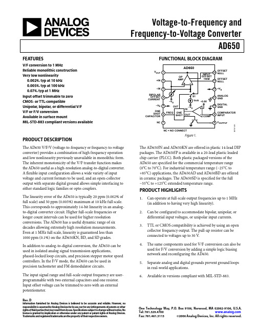
Voltage-to-Frequency and Frequency-to-Voltage ConverterAD650Rev. DInformation furnished by Analog Devices is believed to be accurate and reliable. However , no responsibility is assumed by Analog Devices for its use, nor for any infringements of patents or other rights of third parties that may result from its use. Specifications subject to change without notice. No license is granted by implication or otherwise under any patent or patent rights of Analog Devices. T rademarks and registered trademarks are the property of their respective owners.One Technology Way, P.O. Box 9106, Norwood, MA 02062-9106, U.S.A.Tel: 781.329.4700 Fax: 781.461.3113 ©2006 Analog Devices, Inc. All rights reserved.FEATURESV/F conversion to 1 MHzReliable monolithic construction Very low nonlinearity 0.002% typ at 10 kHz 0.005% typ at 100 kHz 0.07% typ at 1 MHzInput offset trimmable to zero CMOS- or TTL-compatibleUnipolar, bipolar, or differential V/F V/F or F/V conversionAvailable in surface mountMIL-STD-883 compliant versions availableFUNCTIONAL BLOCK DIAGRAM00797-001F OUTPUTCOMPARATOR INPUT DIGITAL GNDANALOG GND +V S OFFSET NULL NC ONE SHOT CAPACITOR–V S BIPOLAR CURRENT–IN +IN V OUT OFFSET NULL NC = NO CONNECTFigure 1.PRODUCT DESCRIPTIONThe AD650 V/F/V (voltage-to-frequency or frequency-to-voltageconverter) provides a combination of high frequency operation and low nonlinearity previously unavailable in monolithic form. The inherent monotonicity of the V/F transfer function makes the AD650 useful as a high-resolution analog-to-digital converter. A flexible input configuration allows a wide variety of input voltage and current formats to be used, and an open-collector output with separate digital ground allows simple interfacing to either standard logic families or opto-couplers.The linearity error of the AD650 is typically 20 ppm (0.002% of full scale) and 50 ppm (0.005%) maximum at 10 kHz full scale. This corresponds to approximately 14-bit linearity in an analog-to-digital converter circuit. Higher full-scale frequencies or longer count intervals can be used for higher resolution conversions. The AD650 has a useful dynamic range of six decades allowing extremely high resolution measurements. Even at 1 MHz full scale, linearity is guaranteed less than 1000 ppm (0.1%) on the AD650KN, BD, and SD grades. In addition to analog-to-digital conversion, the AD650 can be used in isolated analog signal transmission applications,phased-locked loop circuits, and precision stepper motor speed controllers. In the F/V mode, the AD650 can be used in precision tachometer and FM demodulator circuits.The input signal range and full-scale output frequency are user-programmable with two external capacitors and one resistor. Input offset voltage can be trimmed to zero with an external potentiometer.The AD650JN and AD650KN are offered in plastic 14-lead DIP packages. The AD650JP is available in a 20-lead plastic leaded chip carrier (PLCC). Both plastic packaged versions of the AD650 are specified for the commercial temperature range (0°C to 70°C). For industrial temperature range (−25°C to +85°C) applications, the AD650AD and AD650BD are offered in ceramic packages. The AD650SD is specified for the full −55°C to +125°C extended temperature range.PRODUCT HIGHLIGHTS1. Can operate at full-scale output frequencies up to 1 MHz(in addition to having very high linearity). 2. Can be configured to accommodate bipolar, unipolar, ordifferential input voltages, or unipolar input currents. 3. TTL or CMOS compatibility is achieved by using an opencollector frequency output. The pull-up resistor can be connected to voltages up to 30 V . 4. The same components used for V/F conversion can also beused for F/V conversion by adding a simple logic biasing network and reconfiguring the AD650. 5. Separate analog and digital grounds prevent ground loopsin real-world applications. 6. Available in versions compliant with MIL-STD-883.AD650Rev. D | Page 2 of 20TABLE OF CONTENTSFeatures..............................................................................................1 Functional Block Diagram..............................................................1 Product Description.........................................................................1 Product Highlights...........................................................................1 Revision History...............................................................................2 Specifications.....................................................................................3 Absolute Maximum Ratings............................................................5 ESD Caution..................................................................................5 Pin Configurations and Function Descriptions...........................6 Circuit Operation.............................................................................7 Unipolar Configuration...............................................................7 Component Selection...................................................................8 Bipolar V/F..................................................................................10 Unipolar V/F, Negative Input Voltage.....................................10 F/V Conversion..........................................................................10 High Frequency Operation.......................................................10 Decoupling and Grounding......................................................12 Temperature Coefficients..........................................................12 Nonlinearity Specification........................................................13 PSRR.............................................................................................14 Other Circuit Considerations...................................................14 Applications.....................................................................................16 Differential Voltage-to-Frequency Conversion......................16 Autozero Circuit.........................................................................16 Phase-Locked Loop F/V Conversion......................................17 Outline Dimensions.......................................................................19 Ordering Guide.. (20)REVISION HISTORY3/06—Rev. C to Rev. DUpdated Format..................................................................Universal Changes to Product Highlights.......................................................1 Changes to Table 1............................................................................3 Added Pin Function Descriptions Table ......................................6 Updated Outline Dimensions.......................................................18 Changes to Ordering Guide. (19)AD650Rev. D | Page 3 of 20SPECIFICATIONST = 25°C, V S = ±15 V , unless otherwise noted. Table 1.AD650J/AD650A AD650K/AD650B AD650SModelMin Typ Max Min Typ Max Min Typ Max Units DYNAMIC PERFORMANCE Full-Scale Frequency Range 1 1 1 MHz Nonlinearity 1f MAX = 10 kHz 0.002 0.005 0.002 0.005 0.002 0.005 % f MAX = 100 kHz 0.005 0.02 0.005 0.02 0.005 0.02 % f MAX = 500 kHz 0.02 0.05 0.02 0.05 0.02 0.05 % f MAX = 1 MHz0.1 0.05 0.1 0.05 0.1 % Full-Scale Calibration Error 2100 kHz ± 5 ± 5 ± 5 % 1 MHz ± 10 ± 10 ± 10 %vs. Supply 3−0.015 +0.015 −0.015 +0.015 −0.015 +0.015% of FSR/V vs. Temperature A, B, and S Grades at 10 kHz ±75 ±75 ±75 ppm/°C at 100 kHz ±150 ±150 ±200 ppm/°C J and K Grades at 10 kHz ±75 ±75 ppm/°C at 100 kHz±150 ±150 ppm/°C BIPOLAR OFFSET CURRENT Activated by 1.24 kΩ Between Pin 4 and Pin 5 0.45 0.50.55 0.45 0.50.55 0.45 0.50.55 mADYNAMIC RESPONSEMaximum Settling Time for Full-Scale Step Input 1 pulse of new frequency plus 1 μs 1 pulse of new frequency plus 1 μs 1 pulse of new frequency plus 1 μs Overload Recovery Time Step Input1 pulse of new frequency plus 1 μs 1 pulse of new frequency plus 1 μs 1 pulse of new frequency plus 1 μsANALOG INPUT AMPLIFIER (V/F CONVERSION) Current Input Range (Figure 4) 0 +0.6 0 +0.6 0 +0.6 mA Voltage Input Range (Figure 12) −10 0 −10 0 −10 0 V Differential Impedance 2 MΩ||10 pF 2 MΩ||10 pF 2 MΩ||10 pF Common-Mode Impedance 1000 MΩ||10 pF 1000 MΩ||10 pF 1000 MΩ||10 pF Input Bias Current Noninverting Input 40 100 40 100 40 100 nA Inverting Input ±8 ±20 ±8 ±20 ±8 ±20 nA Input Offset Voltage (Trimmable to Zero)±4 ±4 ±4 mV vs. Temperature (T MIN to T MAX ) ±30 ±30 ±30 μV/°C Safe Input Voltage±V S ±V S ±V S V COMPARATOR (F/V CONVERSION) Logic 0 Level −V S −1 −V S −1 −V S −1 V Logic 1 Level0 +V S 0 +V S 0 +V S V Pulse Width Range 4 0.1 (0.3 × t OS ) 0.1 (0.3 × t OS ) 0.1 (0.3 × t OS ) μs Input Impedance250 250 250 kΩ OPEN COLLECTOR OUTPUT (V/F CONVERSION)Output Voltage in Logic 0 I SINK ≤ 8 mA, T MIN to T MAX0.4 0.4 0.4 V Output Leakage Current in Logic 1 100 100 100 nA Voltage Range 5 0 36 0 36 0 36 VAD650Rev. D | Page 4 of 20AD650J/AD650A AD650K/AD650B AD650S Model Min Typ Max Min Typ Max Min Typ Max Units AMPLIFIER OUTPUT (F/V CONVERSION) Voltage Range(1500 Ω Min Load Resistance) 0 10 0 10 0 10 V Source Current(750 Ω Max Load Resistance) 10 10 10 mA Capacitive Load(Without Oscillation) 100 100 100 pF POWER SUPPLY Voltage, Rated Performance ±9 ±18 ±9 ±18 ±9 ±18 V Quiescent Current 8 8 8 mA TEMPERATURE RANGE Rated Performance N Package 0 +70 0 +70 °C D Package −25 +85 −25 +85 −55 +125 °C1 Nonlinearity is defined as deviation from a straight line from zero to full scale, expressed as a fraction of full scale. 2Full-scale calibration error adjustable to zero. 3Measured at full-scale output frequency of 100 kHz. 4Refer to F/V conversion section of the text. 5Referred to digital ground.Specifications shown in boldface are tested on all production units at final electrical test. Results from those tests are used to calculate outgoing quality levels. All min and max specifications are guaranteed, although only those shown in boldface are tested on all production units.AD650Rev. D | Page 5 of 20ABSOLUTE MAXIMUM RATINGSParameter Rating Total Supply Voltage 36 V Storage Temperature Range −55°C to +150°C Differential Input Voltage ±10 V Maximum Input Voltage ±V S Open Collector Output Voltage Above Digital GND 36 V Current 50 mA Amplifier Short Circuit to Ground Indefinite Comparator Input Voltage ±V SStresses above those listed under Absolute Maximum Ratings may cause permanent damage to the device. This is a stress rating only; functional operation of the device at these or any other conditions above those indicated in the operational section of this specification is not implied. Exposure to absolutemaximum rating conditions for extended periods may affectdevice reliability.ESD CAUTIONESD (electrostatic discharge) sensitive device. Electrostatic charges as high as 4000 V readily accumulate on the human body and test equipment and can discharge without detection. Although this product features proprietary ESD protection circuitry, permanent damage may occur on devices subjected to high energy electrostatic discharges. Therefore, proper ESD precautions are recommended to avoid performancedegradation or loss of functionality.AD650Rev. D | Page 6 of 20PIN CONFIGURATIONS AND FUNCTION DESCRIPTIONSV OUTCURRENTOFFSET NULLOFFSET NULL+V SANALOG GND –V SDIGITAL GNDCAPACITORCOMPARATOR INPUT NCF OUTPUT NC = NO CONNECT00797-010Figure 2. D-14, N-14 Pin ConfigurationsNC = NO CONNECT–INNC BIPOLAR OFFSET CURRENTNC –V S +V S NCANALOG GND NCDIGITAL GND+I NV O U TN C O F F S E T N U L L O F F S E T N U L LO N E S H O C A P A C I T O R N CN CF O U T P U TC O M P A R A T O R I N P U T00797-011Figure 3. P-20A Pin ConfigurationTable 2. Pin Function DescriptionsPin No.D-14, N-14 P-20A Mnemonic Description1 2 V OUTOutput of Operational Amplifier. The operational amplifier, along with C INT , is used in the integrate stage of the V to F conversion. 2 3 +IN Positive Analog Input. 3 4 –INNegative Analog Input.4 6 BIPOLAR OFFSET CURRENT On-Chip Current Source. This can be used in conjunction with an external resistor to remove the operational amplifier’s offset.5 8 –V SNegative Power Supply Input.6 9ONE-SHOT CAPACITOR The Capacitor, C OS , is Connected to This Pin. C OS determines the time period for the one shot. 7 1, 5, 7, 10, 11, 15, 17 NC No Connect.8 12 F OUTPUTFrequency Output from AD650.9 13 COMPARATOR INPUT Input to Comparator. When the input voltage reaches −0.6 V, the one shot is triggered.10 14 DIGITAL GND Digital Ground. 11 16 ANALOG GND Analog Ground.12 18 +V SPositive Power Supply Input.13, 1419, 20OFFSET NULLOffset Null Pins. Using an external potentiometer, the offset of the operational amplifier can be removed.AD650Rev. D | Page 7 of 20CIRCUIT OPERATIONUNIPOLAR CONFIGURATIONThe AD650 is a charge balance voltage-to-frequency converter. In the connection diagram shown in Figure 4, or the block diagram of Figure 5, the input signal is converted into an equivalent current by the input resistance R IN . This current is exactly balanced by an internal feedback current delivered in short, timed bursts from the switched 1 mA internal current source. These bursts of current can be thought of as precisely defined packets of charge. The required number of charge packets, each producing one pulse of the output transistor, depends upon the amplitude of the input signal. Because the number of charge packets delivered per unit time is dependent on the input signal amplitude, a linear voltage-to-frequency transformation is accomplished. The frequency output is furnished via an open collector transistor.A more rigorous analysis demonstrates how the charge balance voltage-to-frequency conversion takes place.A block diagram of the device arranged as a V-to-F converter is shown in Figure 5. The unit is comprised of an input integrator, a current source and steering switch, a comparator, and a one shot. When the output of the one shot is low, the currentsteering switch S 1 diverts all the current to the output of the op amp; this is called the integration period. When the one shot has been triggered and its output is high, the switch S 1 diverts all the current to the summing junction of the op amp; this is called the reset period. The two different states are shown in Figure 6 and Figure 7 along with the various branch currents. It should be noted that the output current from the op amp is the same for either state, thus minimizing transients.00797-003–15VOUTLOGICV INFigure 4. Connection Diagram for V/F Conversion, Positive Input Voltage007S+–CFigure 5. Block Diagram00797-005–V SFigure 6. Reset Mode00797-006–V SFigure 7. Integrate Mode00797-007tFigure 8. Voltage Across C INTAD650Rev. D | Page 8 of 20The positive input voltage develops a current (I IN = V IN /R IN ) that charges the integrator capacitor C INT . As charge builds up on C INT , the output voltage of the integrator ramps downward towards ground. When the integrator output voltage (Pin 1) crosses the comparator threshold (–0.6 V) the comparator triggers the one shot, whose time period, t OS is determined by the one-shot capacitor C OS .Specifically, the one-shot time period issec 100.3F /sec 108.673−×+××=OS OS C t (1)The reset period is initiated as soon as the integrator output voltage crosses the comparator threshold, and the integrator ramps upward by an amount(IN INTOS OS I C )t dt dV t V −=×=ΔmA 1 (2)After the reset period has ended, the device starts anotherintegration period, as shown in Figure 8, and starts rampingdownward again. The amount of time required to reach thecomparator threshold is given as()⎟⎟⎠⎞⎜⎜⎝⎛−=−=Δ=1mA 1mA 11IN OS INT N IN INT OSI t C I I C t dt dV VT (3) The output frequency is now given as FC R V A F t I T t f OS IN IN OS IN OS OUT 1104.4/Hz15.0mA11×+×=×=+= (4) Note that C INT , the integration capacitor, has no effect on the transfer relation, but merely determines the amplitude of the sawtooth signal out of the integrator.One-Shot TimingA key part of the preceding analysis is the one-shot time period given in Equation 1. This time period can be broken down into approximately 300 ns of propagation delay and a second time segment dependent linearly on timing capacitor C OS . When the one shot is triggered, a voltage switch that holds Pin 6 at analog ground is opened, allowing that voltage to change. An internal 0.5 mA current source connected to Pin 6 then draws its current out of C OS , causing the voltage at Pin 6 to decrease linearly. At approximately –3.4 V , the one shot resets itself, thereby ending the timed period and starting the V/Fconversion cycle over again. The total one-shot time period can be written mathematically asDELAY GATE DISCHARGE OS OS T I C V t +Δ= (5) substituting actual values quoted in Equation 5, sec 10300A105.0V 4.393−−×+×−×−=OS OS C t (6)This simplifies into the timed period equation (see Equation 1).COMPONENT SELECTIONOnly four component values must be selected by the user. These are input resistance R IN , timing capacitor C OS , logic resistor R2, and integration capacitor C INT . The first two determine the input voltage and full-scale frequency, while the last two aredetermined by other circuit considerations.Of the four components to be selected, R2 is the easiest to define. As a pull-up resistor, it should be chosen to limit the current through the output transistor to 8 mA if a TTLmaximum V OL of 0.4 V is desired. For example, if a 5 V logicsupply is used, R2 should be no smaller than 5 V/8 mA or 625 Ω. A larger value can be used if desired.R IN and C OS are the only two parameters available to set the full- scale frequency to accommodate the given signal range. The swing variable that is affected by the choice of R IN and C OS is nonlinearity. The selection guides of Figure 9 and Figure 10 show this quitegraphically. In general, larger values of C OS and lower full-scale input currents (higher values of R IN ) provide better linearity. In Figure 10, the implications of four different choices of R IN are shown. Although the selection guide is set up for a unipolarconfiguration with a 0 V to 10 V input signal range, the resultscan be extended to other configurations and input signal ranges.For a full-scale frequency of 100 kHz (corresponding to 10 Vinput), among the available choices R IN = 20 kΩ and C OS = 620 pF gives the lowest nonlinearity, 0.0038%. In addition, the highest frequency that gives the 20 ppm minimum nonlinearity isapproximately 33 kHz (40.2 kΩ and 1000 pF). For input signal spans other than 10 V , the input resistance must be scaled proportionately. For example, if 100 kΩ is called out for a 0 V to 10 V span, 10 kΩ would be used with a 0 V to 1 V span, or 200 kΩ with a ±10 V bipolar connection.The last component to be selected is the integration capacitor C INT . In almost all cases, the best value for C INT can be calculated using the equation(minimum pF 1000sec/104)MAXINT f F C −=(7)When the proper value for C INT is used, the charge balance architecture of the AD650 provides continuous integration of the input signal, therefore, large amounts of noise and interference can be rejected. If the output frequency ismeasured by counting pulses during a constant gate period, the integration provides infinite normal-mode rejection forfrequencies corresponding to the gate period and its harmonics. However, if the integrator stage becomes saturated by anexcessively large noise pulse, then the continuous integration ofthe signal is interrupted, allowing the noise to appear at the output.AD650Rev. D | Page 9 of 20If the approximate amount of noise that appears on C INT is known (V NOISE ), then the value of C INT can be checked using the following inequality:NOISES OS INT V V A t C −−+××>−V 31013For example, consider an application calling for a maximum frequency of 75 kHz, a 0 V to 1 V signal range, and supplyvoltages of only ±9 V . The component selection guide of Figure 9 is used to select 2.0 kΩ for R IN and 1000 pF for C OS . This results in a one-shot time period of approximately 7 μs. Substituting 75 kHz into Equation 7 yields a value of 1300 pF for C INT . When the input signal is near zero, 1 mA flows through the integration capacitor to the switched current sink during the reset phase, causing the voltage across C INT to increase by approximately 5.5 V . Because the integrator output stage requires approximately 3 V headroom for proper operation, only 0.5 V margin remains for integrating extraneous noise on the signal line. A negative noise pulse at this time could saturate the integrator, causing an error in signal integration. Increasing C INT to 1500 pF or 2000 pF provides much more noise margin, thereby eliminating this potential trouble spot.1MHz100kHz10kHz501001000F R E Q U E N C Y F U L L -S C A L EC OS (pF)00797-008Figure 9. Full-Scale Frequency vs. C OS10020501001000T Y P I C A L N O N L I N E A R I T Y (p p m )C OS (pF)100000797-009Figure 10. Typical Nonlinearity vs. C OSAD650Rev. D | Page 10 of 20BIPOLAR V/FFigure 11 shows how the internal bipolar current sink is used to provide a half-scale offset for a ±5 V signal range, while providing a 100 kHz maximum output frequency. The nominally 0.5 mA (±10%) offset current sink is enabled when a 1.24 kΩ resistor is connected between Pin 4 and Pin 5. Thus, with the grounded 10 kΩ nominal resistance shown, a −5 V offset is developed at Pin 2. Because Pin 3 must also be at −5 V , the current through R IN is 10 V/40 kΩ = +0.25 mA at V IN = +5 V , and 0 mA at V IN = –5 V . Components are selected using the same guidelines outlined for the unipolar configuration with one alteration. The voltage across the total signal range must be equated to the maximum input voltage in the unipolar configuration. In other words, the value of the input resistor R IN is determined by the input voltage span, not the maximum input voltage. A diode from Pin 1 to ground is also recommended. This is further discussed in the Other Circuit Considerations section.As in the unipolar circuit, R IN and C OS must have low temperature coefficients to minimize the overall gain drift. The 1.24 kΩ resistor used to activate the 0.5 mA offset current should also have a low temperature coefficient. The bipolar offset current has a temperature coefficient of approximately −200 ppm/°C.UNIPOLAR V/F, NEGATIVE INPUT VOLTAGEFigure 12 shows the connection diagram for V/F conversion of negative input voltages. In this configuration, full-scale output frequency occurs at negative full-scale input, and zero output frequency corresponds with zero input voltage.A very high impedance signal source can be used because it only drives the noninverting integrator input. Typical input impedance at this terminal is 1 GΩ or higher. For V/F conversion of positive input signals using the connection diagram of Figure 4, the signal generator must be able to source the integration current to drive the AD650. For the negative V/F conversion circuit of Figure 12, the integration current is drawn from ground through R1 and R3, and the active input is high impedance. Circuit operation for negative input voltages is very similar to positive input unipolar conversion described in the Unipolar Configuration section. For best operating results use Equation 7 and Equation 8 in the Component Selection section.F/V CONVERSIONThe AD650 also makes a very linear frequency-to-voltage converter. Figure 13 shows the connection diagram for F/V conversion with TTL input logic levels. Each time the input signal crosses the comparator threshold going negative, the one shot is activated and switches 1 mA into the integrator input for a measured time period (determined by C OS ). As the frequency increases, the amount of charge injected into the integration capacitor increases proportionately. The voltage across the integration capacitor is stabilized when the leakage current through R1 and R3 equals the average current being switched into the integrator. The net result of these two effects is an average output voltage that is proportional to the inputfrequency. Optimum performance can be obtained by selecting components using the same guidelines and equations listed in the Bipolar V/F section.For a more complete description of this application, refer to Analog Devices’ Application Note AN-279.HIGH FREQUENCY OPERATIONProper RF techniques must be observed when operating the AD650 at or near its maximum frequency of 1 MHz. Lead lengths must be kept as short as possible, especially on the one shot and integration capacitors, and at the integrator summing junction. In addition, at maximum output frequencies above 500 kHz, a 3.6 kΩ pull-down resistor from Pin 1 to −V S isrequired (see Figure 14). The additional current drawn through the pulldown resistor reduces the op amp’s output impedance and improves its transient response.00797-012V ±5V+15VF OUTFigure 11. Connections for ±5 V Bipolar V/F with 0 kHz to 100 kHz TTL Output00797-013+15VLOGICF OUTFigure 12. Connection Diagram for V/F Conversion, Negative Input Voltage00797-014–15VINFigure 13. Connection Diagram for F/V Conversion00797-015+15VOUTVFigure 14. 1 MHz V/F Connection DiagramDECOUPLING AND GROUNDINGIt is effective engineering practice to use bypass capacitors on the supply-voltage pins and to insert small-valued resistors (10 Ω to 100 Ω) in the supply lines to provide a measure of decoupling between the various circuits in a system. Ceramic capacitors of 0.1 μF to 1.0 μF should be applied between the supply-voltage pins and analog signal ground for proper bypassing on the AD650.In addition, a larger board level decoupling capacitor of 1 μF to 10 μF should be located relatively close to the AD650 on each power supply line. Such precautions are imperative in high resolution, data acquisition applications where users expect to exploit the full linearity and dynamic range of the AD650. Although some types of circuits can operate satisfactorily with power supply decoupling at only one location on each circuit board, such practice is strongly discouraged in high accuracy analog design.Separate digital and analog grounds are provided on theAD650. The emitter of the open collector frequency output transistor is the only node returned to the digital ground. All other signals are referred to analog ground. The purpose of the two separate grounds is to allow isolation between the high precision analog signals and the digital section of the circuitry. As much as several hundred millivolts of noise can be tolerated on the digital ground without affecting the accuracy of the VFC. Such ground noise is inevitable when switching the large currents associated with the frequency output signal.At 1 MHz full scale, it is necessary to use a pull-up resistor of about 500 Ω in order to get the rise time fast enough to provide well defined output pulses. This means that from a 5 V logic supply, for example, the open collector output draws 10 mA. This much current being switched causes ringing on long ground runs due to the self-inductance of the wires. For instance, 20 gauge wire has an inductance of about 20 nH per inch; a current of 10 mA being switched in 50 ns at the end of 12 inches of 20 gauge wire produces a voltage spike of 50 mV. The separate digital ground of the AD650 easily handles these types of switching transients.A problem remains from interference caused by radiation of electromagnetic energy from these fast transients. Typically, a voltage spike is produced by inductive switching transients; these spikes can capacitively couple into other sections of the circuit. Another problem is ringing of ground lines and power supply lines due to the distributed capacitance and inductance of the wires. Such ringing can also couple interference into sensitive analog circuits. The best solution to these problems is proper bypassing of the logic supply at the AD650 package. A 1 μF to 10 μF tantalum capacitor should be connected directly to the supply side of the pull-up resistor and to the digital ground (Pin 10). The pull-up resistor should be connected directly to the frequency output (Pin 8). The lead lengths on the bypass capacitor and the pull-up resistor should be as short as possible. The capacitor supplies (or absorbs) the current transients, and large ac signals flows in a physically small loop through the capacitor, pull-up resistor, and frequency output transistor. It is important that the loop be physically small for two reasons: first, there is less self-inductance if the wires are short, and second, the loop does not radiate RFI efficiently. The digital ground (Pin 10) should be separately connected to the power supply ground. Note that the leads to the digital power supply are only carrying dc current and cannot radiate RFI. There can also be a dc ground drop due to the difference in currents returned on the analog and digital grounds. This does not cause any problem. In fact, the AD650 tolerates as much as 0.25 V dc potential difference between the analog and digital grounds. These features greatly ease power distribution and ground management in large systems. Proper technique for grounding requires separate digital and analog ground returns to the power supply. Also, the signal ground must be referred directly to analog ground (Pin 11) at the package. All of the signal grounds should be tied directly to Pin 11, especially the one-shot capacitor. More information on proper grounding and reduction of interference can be found in “Noise Reduction Techniques in Electronic Systems, 2nd edition” by Henry W. Ott, (John Wiley & Sons, Inc., 1988).TEMPERATURE COEFFICIENTSThe drift specifications of the AD650 do not include temperature effects of any of the supporting resistors or capacitors. The drift of the input resistors R1 and R3 and the timing capacitor C OS directly affect the overall temperature stability. In the application of Figure 5, a 10 ppm/°C input resistor used with a 100 ppm/°C capacitor can result in a maximum overall circuit gain drift of:150 ppm/°C (AD650A) + 100 ppm/°C (C OS)+ 10 ppm/°C (R IN) = 260 ppm/°CIn bipolar configuration, the drift of the 1.24 kΩ resistor used to activate the internal bipolar offset current source directly affects the value of this current. This resistor should be matched to the resistor connected to the op amp noninverting input, Pin 2 (see Figure 11). That is, the temperature coefficients of these two resistors should be equal. If this is the case, then the effects of the temperature coefficients of the resistors cancel each other, and the drift of the offset voltage developed at the op amp noninverting input is solely determined by the AD650. Under these conditions, the TC of the bipolar offset voltage is typically −200 ppm/°C and is a maximum of −300 ppm/°C. The offset voltage always decreases in magnitude as temperature is increased.。
LM311 电压比较器
Absolute Maximum Ratings for the LM111
If Military Aerospace specified devices are required please contact the National Semiconductor Sales Office Distributors for availability and specifications (Note 7) Total Supply Voltage (V84) 36V Output to Negative Supply Voltage (V74) Ground to Negative Supply Voltage (V14) Differential Input Voltage Input Voltage (Note 1) Output Short Circuit Duration Operating Temperature Range LM111 LM211 50V 30V g 30V g 15V 10 sec b 55 C to 125 C b 25 C to 85 C
Note Do Not Ground Strobe Pin Output is turned off when current is pulled from Strobe Pin
Increases typical common mode slew from 7 0V ms to 18V ms
Detector for Magnetic Transducer
for the LM111 and LM211 (Note 3) Conditions Min Typ 07 40 60 40 200 200 0 75 20 02 15 50 10 40 20 150 Max 30 10 100 Units mV nA nA V mV ns V mA nA mV nA nA V V mA mA mA
TLE4942中文

Differential Two-Wire Hall Effect Sensor IC差分两线制霍尔效应传感器ICFeatures 特征• Two-wire PWM current interface 两线制PWM电流接口• Detection of rotation direction 转动方向的探测• Airgap diagnosis 空隙诊断位置诊断• Assembly position diagnosis 安装安装位置诊断• Dynamic self-calibration principle 动态自校准• Single chip solution 单芯片解决方案• No external components needed 无需外部元器件• High sensitivity PSSO2-1 高灵敏度PSSO2-1• South and north pole pre-induction possible 合适的南北极前感应• High resistance to piezo effects 高阻抗压电效应• Large operating air-gaps 大的操作空隙• Wide operating temperature range 宽使用温度范围电容• TLE4942C: 1.8nF overmolded capacitor 1.8nF包胶包胶电容The Hall Effect sensor IC TLE4942 is designed to provide information about rotational speed, direction of rotation, assembly position and limit airgap to modern vehicle dynamics control systems and ABS. The output has been designed as a twowire current interface based on a Pulse Width Modulation principle. The sensor operates without external components and combines a fast power-up time with a low cut-off frequency. Excellent accuracy and sensitivity is specified for harsh automotive requirements as a wide temperature range, high ESD robustness and high EMC resilience.State-of-the-art BiCMOS technology is used for monolithic integration of the active sensor areas and the signal conditioning.霍尔效应传感器IC TLE4942 是用于有关转动速度,转动方向,组合位置,现代车辆动力学控制系统和ABS,输出被设计成基于脉宽调制原理的双线电流接口,传感器工作不需要外部元件和combines a fast power-up time with a low cut-off frequency,出色的精度和灵敏度用于自动化设备在一个宽的温度范围内,高静电释放和高电磁兼容能力。
MAX9140EUK+
MAX9140/MAX9141/MAX9142/MAX9144
40ns, Low-Power, 3V/5V, Rail-to-Rail Single-Supply Comparators
General Description
The MAX9140/MAX9141 are single and the MAX9142/ MAX9144 are dual/quad high-speed comparators optimized for systems powered from a 3V or 5V supply. The MAX9141 features latch enable and device shutdown. These devices combine high speed, low power, and Rail-to-Rail® inputs. Propagation delay is 40ns, while supply current is only 150µA per comparator.
Input Hysteresis Input Bias Current Input Offset Current Common-Mode Rejection Ratio Power-Supply Rejection Ratio
VOS
VHYST IB IOS
CMRR PSRR
(Note 4) (Note 5) (Note 6)
VCC = 5.5V (Note 7) 2.7V ≤ VCC ≤ 5.5V
TA = +25°C TA = TMIN to TMAX
0.5
2
4.5
1.5
lm331详解

Versatile Monolithic V/Fs can Compute as Well as Convert with High AccuracyThe best of the monolithic voltage-to-frequency (V/F)con-verters have performance that’s so good it equals or ex-ceeds that of modular types.Some of these ICs can be designed into quite a variety of circuits because they’re notably versatile.Along with versatility and high performance come the advantages that are characteristic of all V/F con-verters,including good linearity,excellent resolution,wide dynamic range,and an output signal that’s easy to transmit as well as couple through an isolator.One of the recently introduced monolithic types,the LM131,has both high performance and a design that’s rather flex-ible.For instance,it can compute and convert at the same time;the computation is a part of the conversion.Among other functions,it can provide the product,ratio and square root of analog inputs.This IC has an internal reference for its conversion circuitry that’s also brought out to a pin,so it’s available to external circuits associated with the converter.Not surprisingly,it turns out that any deviations of the reference,due to process variations and temperature changes have equal and oppo-site effects on the scale factors of the converter and the external circuitry.(This presumes,of course,that the scale factor of the external circuitry is a linear function of voltage.)Precision Relaxation OscillatorBefore looking at some applications,quickly take a look at the basic circuit of an LM131V/F converter (Figure 1).Basically,this IC,like any V/F converter,is a precision relax-ation oscillator that generates a frequency linearly propor-tional to the input voltage.As might be expected,the circuit has a capacitor,C L ,with a sawtooth voltage on it.Generally speaking,the circuit is a feedback loop that keeps this capacitor charged to a voltage very slightly higher than the input voltage,V IN .If V IN is high,C L discharges relatively quickly through R L ,and the circuit generates a high fre-quency.If V IN is low,C L discharges slowly,and the converter puts out a low frequency.When C L discharges to a voltage equal to the input,the comparator triggers the one-shot.The one-shot closes the current switch and also turns on the output transistor.With the switch closed,current from the current source recharges C L to a voltage somewhat higher than the input.Charging continues for a period determined by R T and C T .At the end of this period,the one-shot returns to its quiescent state and C L resumes discharging.Resistor R S sets the amount of current put out by the current source.In fact,the current in pin 1,with the switch on,is identical to the current in pin 2.The latter pin is at a constant voltage (nominally 1.90V),so a given resistor value can set the operating currents.When connected to a high imped-ance buffer,this pin provides a stable reference for external circuits.The open-collector output at pin 3permits the output swing to be different from the converter’s supply voltage,if the load circuit requires.The supplies don’t have to be separate,however,and both the converter and its load can use the same voltage.National Semiconductor Application Note D August 1980Versatile Monolithic V/Fs Can Compute as Well as Convert with High AccuracyAN-D©2002National Semiconductor Corporation Precision Relaxation Oscillator(Continued)Steady as She GoesBy far the simplest of the circuits that make use of the reference output voltage from the LM131is one that simply ties this output pin right back to the signal input.This con-nection is just a V/F converter with a constant input,which makes it a constant-frequency oscillator.Even with thissimple circuit (Figure 2),variations in the reference voltage have two opposite effects that cancel each other out,so the circuit is particularly stable.In this type of circuit,the temperature-dependent internal delays tend to cancel as well,which isn’t true of relaxation oscillators based on op amps or comparators.00874201FIGURE 1.A voltage-to-frequency converter such as this is a relaxation oscillator with a frequency proportional tothe input voltage.Current pulses keep C L ’s average voltage slightly greater than the input voltage.A N -D 2Steady as She Goes(Continued)Resistors R L and R S are best taken from the same batch.(R L must be larger than R S,so it’s made up of two resistors.)By doing this,the tempco tracking,which is the criticalparameter,is five to ten times better than it would be if R Lwere a single30.1kΩresistor.Although the reference output,pin2,can’t be loaded withoutaffecting the converter’s sensitivity,the comparator input,pin7,has a high impedance so this connection does no harm.Frequency stability is typically±25ppm/˚C,even with anLM331,which as a V/F converter is specified only to150ppm/˚C maximum.From20Hz to20kHz,stability is excel-lent,and the circuit can generate frequencies up to120kHz.Although the simplest way of using the reference output is totie it back to the input,the reference can also be bufferedand amplified to supply such external circuitry as a resistivetransducer,which might be a strain gauge or a pot(Figure3).As in the stable oscillator already described,deviations ofthe internal reference voltage from the ideal cause the trans-ducer’s and the converter’s sensitivities to change equally inopposite directions,so the effects cancel.In this circuit,op amp A2buffers and amplifies the constantvoltage at pin2of the converter to provide the5V excitationfor the strain gauge.Amplifier A1,connected as an instru-mentation amplifier,raises the output of the strain gauge to ausable level while rejecting common-mode pickup.A potentiometer-type transducer works just as well with thiscircuit.Its wiper output takes the place of A1’s output asshown at the X.The reference terminal is both a constant voltage output anda current programming input.So far,it’s been shown simplywith one or two resistors going to ground.It is,however,afull-fledged signal input that accepts a signal from a currentsource quite well.3Steady as She Goes(Continued)This extra input is what enables the LM131to compute while converting.For instance,it will convert the ratio of two volt-ages to a frequency proportional to the ratio (Figure 4).The circuit is still a V/F converter,but has two signal inputs,both of them going to rather unorthodox places at that.The in-puts,shown as voltages,are converted to currents by two current pumps (voltage-to-current converters).Of course,if currents of the proper ranges are available,the current pumps aren’t needed.The left current pump,which includes Q1and A1,determines how fast capacitor C L discharges between output pulses.The other pump sets the current in the reference circuit to control the amount of recharge cur-rent when the one-shot fires.Tying the comparator input,pin 7,to the reference pin sets the comparator’s trip point at a constant voltage.To get an idea of how the circuit works,consider first the effect of,for instance,tripling the input voltage,V1.This make C L discharge to the comparator trip point three times as fast,so the frequency triples.Next,consider a givenchange,such as doubling the voltage at the other input,V2.This doubles the recharge current to C L during the fixed-width output pulse,which means C L ’s voltage in-creases twice as much during recharging.Since the dis-charge into Q1is linear (for V1constant),it takes twice as long for C L to discharge —the frequency becomes half of what it was before.Although the current pumps in Figure 4must have negative inputs,rearranging the op amps according to Figure 5makes them accept positive inputs instead.Trimming out the offset in the op amp gives the ratio converter better linearity and accuracy.The trim circuit in Figure 5a needs stable positive and negative supplies for the offset trimmer,while the one in Figure 5b needs only a stable positive supply.Unmarked components in Figure 5b are the same as in Figure 5a .Note that the full-scale range of the current pumps can be changed by varying the value of the input resistor(s).If either of these pump circuits is used with a single positive supply,00874205R1,R2,R3:Stable components with low tempco Q1:β≥330a00874206bFIGURE 5.These current pumps adapt the converter circuits in Figure 4and Figure 6to positive input voltages.Optional offset trimming improves linearity and accuracy,especially with input signals that have awide dynamic range.A N -D 4Steady as She Goes(Continued)the op amp should be a type such as 1/2LM358or 1/4LM324,which has a common-mode range that includes the negative-supply bus.Computing Square Roots ImplicitlyAn analog divider computes the square root of a signal when the signal is fed to the divider’s numerator input,and the output is fed back to the divider’s denominator input.00874207This type of computation is called implicit,because the end result of the computation is only implied,not explicitly stated by the equation that defines the computation.In the implicit square root computing loop described in the text,a V/F converter serves as a divider.Since it’s a con-verter,its inputs are voltages (or currents),but its output is a frequency.To connect its output back to one of its inputs so it will compute a square root means that its output frequency must be converted back to a voltage.This is taken care of by the frequency-to-voltage converter.It’ll Take ReciprocalsTaking the ratio of two inputs —in other words,doing division —is only one of the mathematical operations thatcan be combined with converting.Another one is a special case of division,which is taking reciprocals.In this instance,the numerator (V1in Figure 4)is held constant,and the denominator,V2,changes over a wide range such as one or two decades.In this case,since the frequency is the recip-rocal of the input,the period of the output is proportional to the input.When operated this way,the V2current pump should have an offset trimmer.A constant current circuit is still needed to discharge capacitor C L .Nonlinearity (that is,deviation from the ideal law)with an LM331is a little better than 1%for 10kHz full-scale.Increas-ing C T to 0.1µF reduces the nonlinearity to below 0.2%while decreasing full-scale output to 1kHz.Two inputs can also be multiplied while converting to a frequency.The multiplying converter circuit (Figure 6)that does this has a more elaborate current pump than the ratio circuit of Figure 4.This pump is really two cascaded circuits;it includes op amps A2and A3as well as transistors Q2and Q3.Current from this pump goes to pin 5to control the one-shot’s pulse width.(This current ranges from 13.3µA to 1.33µA.)As in the ratio circuit,the left current pump controls the discharge rate of C L .The other pump,however,controls the one-shot’s pulse width to vary the amount that C L charges during the pulse.If the V2input is close to zero,the current from the pump into pin 5is small,and the one-shot develops a wide pulse.This allows C L to charge quite a bit.It takes a relatively long time for C L to discharge to the comparator threshold,so the resulting frequency is low.As V2goes negative (a greater absolute magnitude),the output fre-quency rises.Op amp A3must have a common-mode range that extends to the positive supply voltage,which the speci-fied types do.Multiplying,dividing and converting can all be done at the same time by combining the V2input current pump of Figure 4with the circuit of Figure 6.If a scale-factor trimmer is needed,R4in Figure 6is a good choice,better than input resistors such as R1or ing the latter as trimmers would make the input impedance of the circuit change with trim setting.Two V/F converter ICs along with some extra circuitry will take the square root of a voltage input.Square root functions are used mostly to simulate natural laws,but also to linearize functions that have a natural square-law relationship.One of the latter is converting differential pressure to flow,where flow is proportional to the square root of differential pressure.AN-D5It’ll Take Reciprocals(Continued)Versatile Pin Functions Give Design FlexibilityTwo features —the reference and the one-shot —of the LM131/LM331V/F converter deserve a closer look because they are the key to its versatility.The simplified schematic of the chip,shown here along with a transducer and the com-ponents needed for a basic V/F converter,will help to illus-trate how these features work.The reference circuit,connected to pin 2,is both a constant voltage output and a current setting,scale-factor control input.The constant voltage can supply external circuitry,such as the transducer,that feeds the converter’s input.One great advantage of using the converter’s internal refer-ence to supply the external circuitry is that any variation in the reference voltage affects the sensitivities of the converter and the external circuitry by equal and opposite amounts,so the effects of the variation cancel.While providing a constant voltage output,pin 2also pro-vides scale-factor,or sensitivity control for the converter.Current supplied to an external circuit by this terminal comes from the supply (V S )through the current mirror and the transistor.The op amp drives this transistor to hold pin 2at a constant voltage equal to the internal reference,which is nominally 1.9V.The current mirror provides a current to the switch that’s essentially identical to that in pin 2.This means that a resistor to ground or a signal from a current source will set the current that is switched to pin 1.In most circuits,a capacitor goes from pin 1to ground,and the switched cur-rent from this pin recharges the capacitor during the pulse from the one-shot.The one-shot circuit is somewhat like the well known 555timer’s circuit.In the quiescent state,the reset transistor is on and holds pin 5near ground.When pin 7becomes more positive than pin 6(or pin 6falls below pin 7),the input comparator sets the flip-flop in the one-shot.The flip-flop turns on the current limited output transistor (pin 3)and switches the current coming from the current mirror to pin 1.The flip-flop also turns off the reset transistor,and the timing capacitor C T starts to charge toward V S .This charge is exponential,and C T ’s voltage reaches 2/3of V S in about00874209FIGURE 6.The product of two input voltages becomes an equivalent frequency in this converter.A current pump thatincludes op amps A2and A3controls the pulse duration of the converter’s internal one-shot.A N -D 6Versatile Pin Functions Give Design Flexibility(Continued)1.1R T C T time constants.(The quantity1.1is−ln0.333...) When pin5reaches this voltage,the one-shot’s comparator resets the flip-flop which turns off the current to pin1,dis-charges C T,and turns off the output transistor.If the voltages at pins6and7still call for setting the flip-flopafter pin5has reached2/3V S,internal logic not shown inthis simplified diagram overrides the reset signal from theone-shot’s own comparator,and the flip-flop stays set.In thisinstance,C T continues charging past2/3V S. 7Root Loop Computes(Continued)As a sign of this condition,when the converter hangs up,the one-shot’s timing node,pin 5,continues to charge well be-yond its normal peak of 2/3V S .As soon as the comparator A2detects this rise,it pulls up voltage V X ,current I 1in-creases,and the loop catches its breath again.After all these nonlinear computations,this last circuit is about as linear as it can be.It’s a precision,ultralinear V/F converter based on an LM331A (Figure 8)that has several detail refinements over previous V/F converter circuits.Choosing the proper components and trimming the tempco give less than 0.02%error and 0.003%nonlinearity for a ±20˚C range around room temperature.This circuit has an active integrator,which includes the op amp and the integrating feedback capacitor,C F .The integra-tor converts the input voltage,which is negative,into a positive-going ramp.When the ramp reaches the converter IC’s comparator threshold,the one-shot fires and switches a pulse of current to the integrator’s summing junction.This current makes the integrator’s output ramp down quickly.When the one-shot times out,the cycle repeats.00874211FIGURE 7.Two converter ICs generate an output frequency proportional to the square root of the input voltage.Thecircuit is an implicit loop in which IC1serves as a divider and V/F converter.This IC’s output goes back to itsdenominator input through F/V converter IC2to make the circuit output equal the input’s square root.A N -D 8Root Loop Computes(Continued)There are several reasons this converter circuit gives high performance:•A feedback limiter prevents the op amp from driving pin7 of the LM331A negative.The limiter circuit arrangement bypasses the leakage through CR5to ground via R5,so it won’t reach the summing junction.Bypassing leakage this way is especially important at high temperatures.•The offset trimming pot is connected to the stable1.9V reference at pin2instead of to a power supply bus that might be unstable and noisy.•A small fraction(180µV,full-scale)of the input voltage goes via R4to the R S network,which improves the non-linearity from0.004%to0.002%.•Resistors R2and R3are the same value,so that resis-tors such as Allen-Bradley type CC metal-film types can provide excellent tempco tracking at low cost.(This track-ing is very good when equal values come from the same batch.)Resistor R1should be a low tempco metal-film or wirewound type,with a maximum tempco of±10ppm/˚C or±25ppm/˚C.In addition,C T should be a polystyrene or Teflon type.Poly-styrene is rated to80˚C,while Teflon goes to150˚C.Both types can be obtained with a tempco of−110±30ppm/˚C. Choosing this tempco for C T makes the tempco,due to C T, of the full-scale output frequency110ppm/˚C.Using tight tolerance components results in a total tempco between0ppm/˚C and220ppm/˚C,so the tempco will never be negative.The voltage at CR1and R X has a tempco of −6mV/˚C,which can be used to compensate the tempco of the rest of the circuit.Trimming R X compensates for the tempco of the V/F IC,the capacitor,and all the resistors.A good starting value for selecting R X is430kΩ,which will give the135µA flowing out of pin2a slope of110ppm/˚C.If the output frequency increases with temperature,a little more conductance should be added in parallel with R X. When doing a second round of trimming,though,note that a resistor of,say, 4.3MΩ,has about the same effect on tempco when shunted across a220kΩresistor that it does when shunted across one of430kΩ,namely,−11ppm/˚C. This technique can give tempcos below±20ppm/˚C or even ±10ppm/˚C.00874212FIGURE8.An ultraprecision V/F converter,capable of better than0.02%error and0.003%nonlinearity for a±20˚C range about room temperature,augments the basic converter with an external integrator.AN-D9Root Loop Computes(Continued)Some precautions help this procedure converge:1.Use a good capacitor for C T .The cheapest polystyrene capacitors will shift in value by 0.05%or more per tem-perature cycle.The actual temperature sensitivity would be indistinguishable from the hysteresis,and the circuit would never be stable.2.After soldering,bake and/or temperature-cycle the cir-cuit (at a temperature not exceeding 75˚C if C T is poly-styrene)for a few hours,to stabilize all components and to relieve the strains from soldering.3.Don’t rush the trimming.Recheck the room temperaturevalue,before and after the high temperature data aretaken,to ensure that hysteresis per cycle is reasonably low.4.Don’t expect a perfect tempco at −25˚C if the circuit istrimmed for ±5ppm/˚C between 25˚C and 60˚C.If it’s been trimmed for zero tempco while warm,none of its components will be linear to much better than 5ppm/˚C or 10ppm/˚C when it’s cold.The values shown in this circuit are generally optimum for ±12V to ±16V regulated supplies but any stable supplies between ±4V and ±22V would be usable,after changing a few component values.LIFE SUPPORT POLICYNATIONAL’S PRODUCTS ARE NOT AUTHORIZED FOR USE AS CRITICAL COMPONENTS IN LIFE SUPPORT DEVICES OR SYSTEMS WITHOUT THE EXPRESS WRITTEN APPROVAL OF THE PRESIDENT AND GENERAL COUNSEL OF NATIONAL SEMICONDUCTOR CORPORATION.As used herein:1.Life support devices or systems are devices or systems which,(a)are intended for surgical implant into the body,or (b)support or sustain life,and whose failure to perform when properly used in accordance with instructions for use provided in the labeling,can be reasonably expected to result in a significant injury to the user.2.A critical component is any component of a life support device or system whose failure to perform can be reasonably expected to cause the failure of the life support device or system,or to affect its safety or effectiveness.National Semiconductor Corporation AmericasEmail:support@National Semiconductor EuropeFax:+49(0)180-5308586Email:europe.support@Deutsch Tel:+49(0)6995086208English Tel:+44(0)8702402171Français Tel:+33(0)141918790National Semiconductor Asia Pacific Customer Response Group Tel:65-2544466Fax:65-2504466Email:ap.support@National Semiconductor Japan Ltd.Tel:81-3-5639-7560Fax:81-3-5639-7507A N -DV e r s a t i l e M o n o l i t h i c V /F s C a n C o m p u t e a s W e l l a s C o n v e r t w i t h H i g h A c c u r a c yNational does not assume any responsibility for use of any circuitry described,no circuit patent licenses are implied and National reserves the right at any time without notice to change said circuitry and specifications.。
DL750高级网络和PC连接Web服务器功能说明书
Advanced Networking and PC ConnectivityWeb Server FunctionsConnect the DL750 to your PC through the Ethernet connection. This allows for easy remote operation using Internet Explorer.FTPY ou can easily copyand paste files to andfrom a PC and theThe Wirepuller softwareprogram displays a screenimage of the DLon your PC so that you canmonitor waveform signals.In addition, you can use thePC’s mouse and keyboardHigh-Speed 10 MS/s 12-Bit Isolation Module (701250)Input channels2Input couplings AC, DC, GNDMaximum sampling rate10 MS/sA/D conversion resolution12 bits (150 LSB/div)Input type Isolated unbalancedFrequency range(–3 dB)1DC, up to 3 MHzInput range(10:1)50 mV/div to 200 V/div (in steps of 1, 2, or 5),(1:1) 5 mV/div to 20 V/div (in steps of 1, 2, or 5) Effective measurement range20 div (display range: 10 div)DC offset±5 divMaximum input voltage (1 kHz or less)In combination with 700929 (10:1) 2600 V (DC + ACpeak)Direct input (1:1) 6, 10250 V (DC + ACpeak)Maximum allowable in-phase voltageIn combination with 700929 (10:1) 3400 Vrms (CA T I), 300 Vrms (CA T II) In combination with 7019in steps of 1, 2, or 5+701954 (1:1) 9400 Vrms (CA T I), 300 Vrms (CA T II) Main unit only (1:1) 1142 V (DC + ACpeak) (CA T I and CAT II, 30 Vrms) DC accuracy1±(0.5% of 10 div)Input impedance 1 MΩ± 1%, approx. 35 pFConnector type Isolation type BNC connectorInput filter OFF, 500 Hz, 5 kHz, 50 kHz, 500 kHz Temperature coefficientZero point±(0.05% of 10 div)/°C (typical value)Gain±(0.02% of 10 div)/°C (typical value)High-Speed 1 MS/s 16-Bit Isolation Module (701251)Input channels2Input couplings AC, DC, GNDMaximum sampling rate 1 MS/sA/D conversion resolution16 bits (2400 LSB/div)Input type Isolated unbalancedFrequency range (–3 dB)1DC, up to 300 kHz (20 V/div to 5 mV/div)Input range(10:1)10 mV/div to 200 V/div (in steps of 1, 2, or 5)(1:1) 1 mV/div to 20 V/div (in steps of 1, 2, or 5) Maximum input voltage (1 kHz or less)In combination with 700929 (10:1) 2600 V (DC + ACpeak)Direct input (1:1) 6, 10140 V (DC + ACpeak)Maximum allowable in-phase voltageIn combination with 700929 (10:1) 3400 Vrms (CA T I), 300 Vrms (CA T II) In combination with 701901+701954 (1:1) 9400 Vrms (CA T I), 300 Vrms (CA T II)Main unit only (1:1) 1142 V (DC + ACpeak) (CA T I and CAT II, 30 Vrms) DC accuracy15 mV/div to 20 V/div±(0.25% of 10 div)2 mV/div±(0.3% of 10 div)1 mV/div±(0.5% of 10 div)Input impedance 1 MΩ± 1%, approx. 35 pFConnector type Isolated type BNC connectorInput filter OFF, 400 Hz, 4 kHz, 40 kHzTemperature coefficientZero point 5 mV/div to 20 V/div: ±(0.02% of 10 div)/°C (typical value)2 mV/div: ±(0.05% of 10 div)/°C (typical value)1 mV/div: ±(0.10% of 10 div)/°C (typical value)Gain 1 mV/div to 20 V/div: ±(0.02% of 10 div)/°C (typical value) High-Speed 10 MS/s 12-Bit Non-Isolation Module (701255)Input channels2Input couplings AC, DC, GNDMaximum sampling rate10 MS/sA/D conversion resolution12 bits (150 LSB/div)Input type Non-isolated unbalancedFrequency range (–3 dB)1DC, up to 3 MHzInput range(10:1)50 mV/div to 200 V/div (in steps of 1, 2, or 5)(1:1) 5 mV/div to 20 V/div (in steps of 1, 2, or 5) Effective measurement range20 div (display range 10 div)DC offset±5 divMaximum input voltage (1 kHz or less)In combination with 701940 (10:1)600 V (DC + ACpeak)Direct input (1:1)250 V (DC + ACpeak)DC accuracy1±(0.5% of 10 div)Input impedance 1 MΩ± 1%, approx. 35 pFConnector type Metal type BNC connectorInput filter OFF, 500 Hz, 5 kHz, 50 kHz, 500 kHz Temperature coefficientZero point±(0.05% of 10 div)/°C (typical value)Gain±(0.02% of 10 div)/°C (typical value)Adaptive passive probe (10:1)701940High-Voltage 100 kS/s 16-Bit Isolation Module (with RMS) (701260)Input channels2Input couplings AC, DC, GND, AC-RMS, DC-RMSMaximum sampling rate100 kS/sA/D conversion resolution16 bits (2400 LSB/div)Input type Isolated unbalancedFrequency range (–3 dB)1Waveform measurement modeDC, up to 40 kHzRMS measurement mode DC, 40 Hz to 10 kHzInput range(10:1)200 mV/div to 2000 V/div (in steps of 1, 2, or 5)(1:1)20 mV/div to 200 V/div (in steps of 1, 2, or 5) Effective measurement range20 div (display range 10 div)DC offset±5 divMaximum input voltage (1 kHz or less)In combination with 700929 (10:1) 21000 V (DC + ACpeak)In combination with 701901+701954 (1:1) 6850 V (DC + ACpeak)Maximum allowable in-phase voltageIn combination with 700929 (10:1)H side: 1000 Vrms (CAT II) 4, L side: 400 Vrms (CAT II) 5In combination with 701901+701954 (1:1)H side: 700 Vrms (CA T II) 7, L side: 400 Vrms (CA T II) 8Direct input (when using a cable which doesn’t comply with the safety standard)H/L sides: 30 Vrms (42 V DC + ACpeak)11 DC accuracy (waveform measurement mode)1±(0.25% of 10 div)DC accuracy (RMS measurement mode)1±(1.0% of 10 div)AC accuracy (RMS measurement mode)1Sine wave input±(1.5% of 10 div)Crest factor of 2 or less±(2.0% of 10 div)Crest factor of 3 or less±(3.0% of 10 div)Input impedance 1 MΩ± 1%, approx. 35 pFConnector type Isolated type BNC connectorInput filter OFF, 100 Hz, 1 kHz, 10 kHzT emperature coefficient (waveform measurement mode)Zero point±(0.02% of 10 div)/°C (typical value)Gain±(0.02% of 10 div)/°C (typical value) Response time (RMS mode)Rise (0 to 90% of 10 div)100 ms (typical)Fall (100 to 10% of 10 div)250 ms (typical)Crest factor (only at RMS measurement)3 or less*Please use 701901 (1:1 safety adaptor lead) or 700929 (10:1 safety probe), which complies with the safety standard, for high-voltage input.*It is very dangerous to use cables that do not comply with the safety standard.Temperature/High-Precision Voltage Module (701265)Input channels2Input couplings TC (thermocouple), DC, GNDInput type Isolated unbalancedApplicable sensors (input coupling: TC)K, E, J, T, L, U, N, R, S, B, W, iron-doped gold/chromel Data updating rate500 HzFrequency range (-3 dB)1DC, up to 100 HzVoltage accuracy1 (at voltage mode)±(0.08% of 10 div + 2 µV)T emperature measurement accuracy 1, 12Type Measured range AccuracyK–200°C to 1300°C±(0.1% of reading + 1.5°C)E–200°C to 800°C except –200 to 0°C:J–200°C to 1100°C±(0.2% of reading + 1.5°C) T–200°C to 400°CL–200°C to 900°CU–200°C to 400°CN0°C to 1300°CR, S0°C to 1700°C±(0.1% of reading + 3°C)except0 to 200°C: ±8°C200 to 800°C: ±5°C B0°C to 1800°C±(0.1% of reading + 2°C),except 400 to 700°C: ±8°CEffective range: 400 to 1800°C W0°C to 2300°C±(0.1% of reading + 3°C)Iron-doped gold/chromel0 to 300 K0 to 50 K: ±4 K50 to 300 K: ±2.5 KMaximum input voltage (1 kHz or less)42 V (DC + ACpeak) (CAT I and CA T II, 30 Vrms)Input range (for 10 div display)100 µV/div to 10 V/div (in steps of 1, 2, or 5) Input connector Binding postInput impedance Approx. 1 MΩInput filter OFF, 2 Hz, 8 Hz, 30 HzT emperature coefficient (for voltage)Zero point±((0.01% of 10 div)/°C + 0.05 µV)/°C (typical value)Gain±(0.02% of 10 div)/°C (typical value) Strain Module (NDIS) (701270)Input channels2Input types DC bridge input (automatic balancing), balanceddifferential input, DC amplifier (floating) Automatic balancing method Electronic auto-balanceAutomatic balancing range±10,000 µSTR (1 gauge method)Bridge voltages Select from 2 V, 5 V, or 10 VGauge resistances120 to 1000 Ω (bridge voltage of 2 V)350 to 1000 Ω (bridge voltage of 2/5/10 V) Gauge rate 1.90 to 2.20 (variable in steps of 0.01)A/D resolution16 bits (4800 LSB/div: Upper=ϩFS, Lower=–FS) Maximum sampling rate100 kS/sFrequency range (–3 dB)1DC, up to 20 kHzDC accuracy1±(0.5% of FS + 5 µSTR)Measurement range/measurable rangeMeasurement range (FS)Measurable range (–FS to +FS)500 µSTR–500 µSTR to 500 µSTR1000 µSTR–1000 µSTR to 1000 µSTR2000 µSTR–2000 µSTR to 2000 µSTR5000 µSTR–5000 µSTR to 5000 µSTR10,000 µSTR–10,000 µSTR to 10,000 µSTR20,000 µSTR–20,000 µSTR to 20,000 µSTRmV/V range support mV/V range = 0.5 ϫ (µSTR range/1000)Maximum allowable input voltage (1 kHz or less)10 V (DC + ACpeak)Maximum allowable in-phase voltage42 V (DC + ACpeak) (CAT I and CA T II, 30 Vrms)T emperature coefficientZero point±5 µSTR/°C (typical value)Gain±(0.02% of FS)/°C (typical value)Internal filter OFF, 1 kHz, 100 Hz, 10 HzInput connector NDIS standardAccessory (a set of connector shell for solder connection)2 NDIS connectors (A1002JC)Recommended bridge head (NDIS type) (sold separately)701955 (bridge resistance of 120 Ω) (w/ 5 m cable)701956 (bridge resistance of 350 Ω) (w/ 5 m cable)10Alligator clip (701954)Isolated probe (700929)Safety adaptor lead (701901)Earphone Mic (w/ PUSH switch) (701951)701280 Frequency Module■ Frequency Measurement SectionInput channels2Data update rate25 kHz (40 µs)Measurement range(frequency)0.01 Hz–200 kHz0.1 Hz/div–50 kHz/divHighest measurement resolution50 ns (20 MHz)■ Input SectionCompatible input signals Encoder pulse input of up to ±42 V,Electromagnetic pickup input 6AC power input up to 300 Vrms (700929 Isolation Probe required) Input type Isolated, unbalancedInput coupling AC,DCInput voltage (1:1)±1 V–±50 V (6 ranges, 1-2-5 steps)(10:1)±10 V–±500 V (6 ranges, 1-2-5 steps)Max input voltage (1 kHz or less)When combined with 700929 (10:1) 2420 V (DC+ACpeak)Direct input (1:1) 1042 V (DC+ACpeak)Max allowable common mode voltageWhen combined with 700929 (10:1) 3300 Vrms (CAT II)Direct input (1:1) 1142 V (DC+ACpeak) 30 Vrms (CAT II)Input impedance: 1 MΩ±1%, approx. 35 pFConnector type Isolated BNC connectorInput filters OFF/100 Hz/1 KHz/10 KHz/100 KHzInput pullup function (ON/OFF)Supports open collector, mechanical contact output, 4.7 KΩ(+5 V) Input chatter suppression (ON/OFF)Setting range 1 ms–1000 msComparator section Presets Logic (5 V/3 V/12 V/24 V), electromagnetic pickup, zero-cross,pullup (5 V), AC100 V, AC200 V, user-definedThreshold range±FS range, resolution in units of 1%Hysteresis±1%, ±2.5%, or ±5% of FSLED display (each CH)ACT (green)Operational status (illuminates during pulse input)OVER (red)Overdrive status (illuminates during an input overrange) Compatible probes/cables(10:1 probe) 700929/701940 (1:1 cable) 366926■ Measurement Function DetailsMeasurable items Frequency (Hz), rpm, rps, Period (sec), Duty (%), Power supplyfreq. (Hz), Pulse width (sec), Pulse integration, Velocity Effective measurement range20 div (10 div display range)Resolution of measured data16 bit (2400 LSB/div)Measurement items and rangesMeasured Item Measurement Range RangeFrequency (Hz)0.01 Hz–200 kHz0.1 Hz/div–50 kHz/divrpm0.01 rpm–100,000 rpm0.1 rpm/div–10,000 rpm/divrps0.001 rps–2000 rps0.01 rps/div–200 rps/divPeriod (sec) 5 µs–50 s10 µs/div–5 s/divDuty (%)0%–100%1%/div–20%/divPower supply freq (Hz)(50 Hz, 60 Hz, 400 Hz)±20 Hz0.1 Hz/div–2 Hz/divPulse width (sec) 2 µs–50 s10 µs/div–5 s/divPulse integration up to 2ϫ109 count100ϫ10-21/div–500ϫ1018/divVelocity Same as freq. (can be converted to km/h and other units) Auxiliary M easurement Functions■ Smoothing Filter Apply moving average to smooth stair step shaped waveforms.(moving average)Moving average constant is specified from 0.2 ms to 1000 msec(moving average constant=specified time ÷40 µs) This reduces jitterand increases the resolution.■ Pulse Average Function Measure the specified number of pulses at once, and specify 1 to4096 pulses for the average value output mode. This has the exactsame effect as the smoothing filter, but averaging can be performedat the pulse interval. Even if encoder gaps are unequal, you canmeasure pulses together and average them.■ Deceleration Prediction A measuring function that automatically compensates for the lack of (Braking Applications)encoder pulse information during deceleration and hypothesizes adeceleration curve.■ Stop Prediction Predicts stop from a specified time after pulse stop(Braking Applications)(set up to 10 stages).■ Offset Observation Function Set an observational center, then zoom and display surroundingarea (for fluctuation observation)Offset setting range = (1 div ϫ 1000)■ M easurement Accuracy 1 5■ Frequency/Revolution/Velocity MeasurementsM easurement accuracy±( 0.05% of 10 div + accuracy depending on the input frequency) Accuracy depending on the input frequency 1 Hz–2 kHz:0.05% of input waveform freq +1 mHz2 kHz–10 kHz:0.1% of input waveform freq10 kHz–20 kHz0.3% of input waveform freq20 kHk–200 kHz0.5% of input waveform freq■ Period MeasurementM easurement accuracy±( 0.05% of 10 div + accuracy depending on the input period) Accuracy depending on the input period500 µs–50 s0.05% of input waveform interval100 µs–500 µs0.1% of input waveform interval50 µs–100 µs0.3% of input waveform interval5 µs–50 µs0.5% of input waveform interval + 0.1 µs■Duty MeasurementAccuracy depending on the input frequency0.1 Hz–1 kHz±0.1% of 100%1 kHz–10 kHz±0.2% of 100%10 kHz–50 kHz±1.0% of 100%50 kHz–100 kHz±2.0% of 100%100 kHz–200 kHz±4.0% of 100%■Pulse Width MeasurementM easurement accuracy±( 0.05 % of 10 div + accuracy depending on the input pulse width) Accuracy depending on the input pulse width500 µs–100 s0.05% of input waveform pulse width100 µs–500 µs0.1% of input waveform pulse width50 µs–100 µs0.3% of input waveform pulse width2 µs–50 µs0.5% of input waveform pulse width + 0.1 µs■Power Supply Frequency MeasurementM easurement accuracy Center freq. at 50, 60 Hz, accuracy of ±0.03 Hz, resolution of 0.01 HzCenter freq. at 400 Hz, accuracy of ±0.3 Hz, resolution of 0.01 Hz 1Under standard operating conditions: (temperature 23˚C±5˚C, humidity 55%±10% RH, warmup of at least 30 minutes, and after calibration.)5Given a minimum input of 0.2 Vpp. M easurement conditions:■During freq./Period measurement: 1 Vpp/1µs square wave input (range=±10 V, bandwidth=FULL,hysteresis=±1%)■During Duty/pulse width measurement: 1 Vpp/5 ns square wave input (range=±10 V, bandwidth=FULL, hysteresis=±1%)■During power supply frequency measurement: 90 Vrms sinewave input (range=AC100 V, BW=100 kHz)6Electromagnetic pickup: given output within 0.2 Vpp–42 Vpp. Minimum sensitivity=0.2 V (at 1:1), connected with 1:1 cable. For types that requires a power supply or terminal resistance, apply it to the sensor side 700929In combination with 700929HL3524HLBNC1110Direct input(With a cable which doesn’t comply with the safety standard)701275 Acceleration/Voltage Module (with AAF)Input channels2Input format Switchable between acceleration and voltage inputAAF (anti-aliasing filter) supports both acceleration and voltage Input coupling(AC coupling for acceleration) ACCL, (voltage) AC,DC,GND Max sampling rate100 kS/sA/D conversion resolution16-bit (2400 LSB/div)Input type Isolated, unbalancedFrequency band (-3 dB)1(acceleration) 0.4 Hz–40 kHz (voltage) DC–40 kHzAC coupling (-3 dB point)acceleration/voltage0.4 Hz or lessInput rangeFor acceleration (±5 V=X1 range)X0.1–X1–X100 (1-2-5 steps)For voltage (10:1)50 mV/div–100 V/div (1-2-5 steps) 12For voltage (1:1) 5 mV/div–10 V/div (1-2-5 steps) 12Effective measuring range20 div (10 div display range)DC offset±5 divMax input voltage (1 kHz or less) 1242 V (DC+ACpeak)Max allowable common mode voltage 1142 V (DC+ACpeak) 30 Vrms (CAT II)Accuracy 1For voltage (DC accuracy)±(0.25% of 10 div)For acceleration (AC accuracy)±(0.5% of 10 div) (at 1 kHz)Input impedance 1 MΩ±1%, approx. 35 pFConnector type Metal BNC connectorInput filters OFF/Auto (AAF)/4 kHz/400 Hz/40 HzAnti-aliasing filter (AAF)Cutoff frequency 13fc (cutoff frequency)=fs (sampling frequency) ϫ 40%fc automatically moves to the sampling frequency.Cutoff characteristics-65dB at 2Xfc (Typical)Temperature coefficient (for voltage) 14Zero point±( 0.02% of 10 div )/ ˚C (Typical)Gain±( 0.02% of 10 div )/ ˚C (Typical)Acceleration sensor bias constant current drive =4 mA±10%, voltage < 22 VExample of compatible acceleration sensor: 15Built-in amp type: Kistler Piezotron™, PCB ICP™, Endevco: Isotron2™Something that supports acceleration sensor and bias is 4 mA/22 V Sensor usage Notes:The sensor is highly sensitive to heat and shocks. If changes intemperature or shocks occur that are outside of the standardoperating conditions, measurement may not be possible for severalminutes.Compatible probes/cables for voltage(10:1 probe) 701940/700929 (1:1 cable) 3669261Under standard operating conditions: (temperature 23˚C±5˚C, humidity 55%±10%RH, warmup of at least 30 minutes, and after Calibration.)12The module’s insulation is functional insulation. Even when using a probe, input above 42 V is not considered safe.13when fs= 50 Hz–100 kHz , (when fs <=50 Hz , fc is fixed to 20 Hz)14 excludes AUTO Filter15Piezotron is a registered trademark of Kistler Instrument Corp.. ICP is a registered trademark of PCB Piezotronics Inc.. ISOTRON2 is a registered trademark of ENDEVCO Corp..For detailed specifications and updated information. /tm/DL750/2. Choose only one.3. Zip drive and DC12V power supply cannot be specified together with the DL750P .4. Cannot be specified together.6. The latest firmware for the DL750 series is available on our Web site./tm/DL750/7.Only supported by the initially-released DL750P (ver. 5.01 or later).DL750 support to be offered by 3rd quarter 2005 (ver. 6.01 or later)Universal (Voltage/Temperature) Modules (701261/701262)DL750/DL750P Accessories DL750/DL750P Model Numbers and Suffix CodesPlug-in Module Model Numbers 52. 42 V is safe when using the 701940 with a Non isolated type BNC input.3. The number of current probes that can be powered from the main unit probe power is limited. See the following for details. /tm/probe/4. There is no limit to the number of externally powered probes that can be used.5. One of each connection lead (B9879PX and B9879KX) is included.Input channels 2Input signals Voltage or temperature (thermocouple)AAF (anti-aliasing filter)701261: none, 701262: includedInput couplings TC (thermocouple), DC, AC, GNDInput typesI Isolated unbalancedMaximum sampling rate Voltage 100 kS/sData updating rate Temperature 500 HzA/D conversion resolution Voltage: 16 bits (2400 LSB/div); temperature: 0.1°CFrequency range (-3 dB)Voltage DC to 40 kHzTemperature DC to 100 HzInput range Voltage (1:1) 5 mV/div to 20 V/div (10 div display, in steps of 1-2-5)Temperature K, E, J, T , L, U, N, R, S, B, W, iron-doped gold/chromelEffective measurement range (voltage)20 div (display range 10 div)DC offset (voltage)±5 divDC accuracy (voltage)±(0.25% of 10 div)Temp. measured range/accuracy T ype Measured Range AccuracyK -200°C to 1300°C ±(0.1% of reading + 1.5°C)E -200°C to 800°C However, for -200°C to 0°C,J -200°C to 1100°C ±0.2% of reading + 1.5°C)T -200°C to 400°CL -200°C to 900°CU -200°C to 400°CN 0°C to 1300°CR, S 0°C to 1700°C ±(0.1% of reading + 3°C)However, 0°C for 200°C: ±8°C200°C for 800°C: ±5°CB 0°C to 1800°C ±(0.1% of reading + 2°C)However, 400°C to 700°C: ±8°CEffective range.: 400°C to 1800°CW 0°C to 2300°C ±(0.1% of reading + 3°C)50 to 300 K: ±2.5 KMax. input voltage (1 kHz or less)42 V (DC+ACpeak): for satisfying safety standards150 V (DC+ACpeak): allowable maximum4Max. allowable common mode volt.42 V (DC+ACpeak) (CA T I & CAT II, 30 Vrms)(1 kHz or less)Input connector Binding postInput impedance Approximately 1 M ΩInput filters Voltage OFF , AUTO (AAF), 4 kHz, 400 Hz, 40 Hz (-12 dB/oct except AUTO)Temperature OFF , 30 Hz, 8 Hz, 2 HzAAF (anti-aliasing filter)701262 only Cutoff frequency fc = fs (sampling frequency) ҂ 40%fc automatically linked with the sampling frequency.Cutoff characteristics: -65 dB at 2 Xfc (typical value)Temp. coefficient (for voltage)Zeropoint ±(0.01% of 10 div)/°C (typical value)Gain ±(0.02% of 10 div)/°C (typical value)Compatible cable 366961 (banana-to-alligator 1:1)1.Under reference operating conditions (ambient temp. of 23°C ±5°C, ambient humidity of 55% ±10%RH, after 30-minute warmup period and calibration).2.Does not include reference junction/temperature compensation accuracy.3.Since the input connecter is of a binding post type, it is possible to touch the metal part of the connector.Therefore, for safety reasons, the maximum value is 42 V (DC+ACpeak).4.Maximum value at which the input circuit will not be damaged.5.When fs= 50 Hz to 100 KHz. When fs ≤50 Hz, fc=20 Hz (fixed).6.Except when filters set to AUTO.Zip is a registered trademark of Iomega Corporation in the United States and/or other countries. Other company names and product names appearing in this document are trademarks or registered trademarks of their respective companies.。
10bit500MS_sPipeline-SARADC的设计
摘要模数转换器(ADC)作为现代通信系统中的关键电路,其性能直接决定了通信系统的整体性能。
在需要中等精度高速ADC的应用场合,如无线网802.11ac通信协议等,流水线逐次逼近型模数转换器(Pipeline-SAR ADC)以其兼顾高速和低功耗的结构特点、对先进工艺兼容良好等优良特性被广泛使用。
针对现代高速通信系统的应用场合,论文设计了一款10bit 500MS/s的Pipeline-SAR ADC,其系统架构为两级结构,两级SAR ADC都实现6bit的数据量化,级间放大器提供4倍增益,设置2bit 级间冗余。
在第一级SAR ADC中,提出了一种基于自关断比较器的非环路(Loop-unrolled)结构,在每位比较完成后,通过自关断信号将当前位比较器关断,在不影响比较器锁存级保持数据的前提下,极大减小了Loop-unrolled结构的功耗;同时,针对Loop-unrolled结构多个比较器之间的失调失配,采用了一种基于参考比较器的后台失调校准方法,参考比较器的引入使得该校准方法可以在不增加额外校准时间的前提下完成后台校准,保证了系统的高速特性。
级间放大器采用了一种增益稳定的动态放大器,通过将动态放大器的增益构造为同种参数比例乘积的形式,实现增益稳定,并对其工作时序进行了优化,避免了额外时钟相的引入。
第二级SAR ADC采用了两路交替比较器结构,同时对两个比较器采用了前台失调校准,以避免引入额外的校准时间。
由于级间放大器仅提供4倍增益,第二级的量化范围较小,本文在第二级电容阵列的设计上使用了非二进制冗余,以减小DAC建立误差造成的影响。
本文还设计了数字码整合电路、全局时钟产生电路,以保证整个Pipeline-SAR ADC设计的完整性。
本文基于TSMC 40nm CMOS工艺设计了具体的电路与版图。
后仿真结果表明,在1.1V电源电压下,采样率为500MS/s时,输入近奈奎斯特频率的信号,在tt工艺角下,有效位数(ENOB)达到9.2位,无杂散动态范围(SFDR)达到64.5dB,功耗为7.52mW,FoM值为25.76fJ/conv.step,达到设计指标要求。
DAQBOARD数据采集板系列产品说明书
The DAQBOARD family of data acquisition boards offers more signal conditioning choices than any comparable product, while also providing high-speed performance and low price. These ISA-bus boards offer 10 µsec per-channel, 16-bit measurement capacity over their 16analog input channels and maintain the same performance when expanded up to 256 channels.Moreover, both the boards’ 16 built-in and 256 expansion channels can each be programmed for a different,dynamically selectable gain. This means that a single DAQBOARD can measure various signal types, from thermocouples to strain-gages, while maintaining the 10µsec per-channel rate. Most other data acquisition boards suffer significant speed and performance declines when equipped with expansion channels, because their on-board sequencing supports only built-in channels.The DAQBOARD family’s 256-channel expansion capacity includes low-cost, compact signal conditioning boards for measuring temperature, voltage, and strain, as well as boards for performing isolation, low-pass filtering, and simultaneous sample and hold. These boards can behoused in similarly inexpensive and compact three- or ten-slot enclosures.FLEXIBLE TRIGGERINGThe DAQBOARDs offer an array of both analog and digital triggering capabilities. For example, the units permit you to trigger on the analog input level from any one channel, and also allow you to program the slope and polarity of the trigger level. Because the DAQBOARDS feature ahardware-based trigger, they minimize trigger latency to less than 10 µs. In contrast, most plug-in boards thatemploy software-polling triggers have typical trigger-to-A/D conversion latencies of 100 µs or more. The DAQBOARDs can also be triggered from a TTL-level digital input or from a command from the PC. Pre-trigger data can be collected using any analog channel as the triggering event.ߜ16-bit A/Dߜ100K Reading/sec Real-time Storage-to-Diskߜ8 Differential- or 16 Single-Ended Inputs, Expandable to 256ߜX1, 2, 4, or 8 Programmable Gain (Other Gains Available with Option Cards)ߜExpansion Cards for High Voltage/current,Strain Gage,Thermocouple, Isolation, Filtering and Simultaneous Sample and Holdߜ512-location Scan Memory for User-Defined Channel/Gain SequencingߜAnalog, Digital, or Software Trigger ߜTwo 12-bit Analog Outputs, 100kHz via On-board DMA or FIFOߜ24 General-Purpose Digital I/O Lines,Expandable to 192ߜ16 High-speed Digital-Input Lines,Scannable at up to 100kHz ߜFive Programmable 16-bit Counter/timersData Acquisition Boards For Desktop PCs$1095Basic SystemShown smaller than actual size.The DAQBOARD is no longer available. Please see the OMB-DAQBOARD-2000 as a substitute or contact salesreceived pulses is accumulated, permitting pulse accumulation concurrently with the measurement ofanalog input channels. The units also permit the width of a digital input pulse to be measured on each channel, with resolution to 1 µs.PULSE/FREQUENCY OUTPUTIn pulse/frequency output modes, the DAQBOARD-200’s five counter-timer channels can each be independently programmed to perform one of several functions. In the pulse generation mode, a single pulse of programmable width can be generated from dc to 500 kHz. In the frequency-generation mode, the DAQBOARDs can generate a square wave of duty cycle from 0.0005% to 99%, with frequencies up to 1 MHz.An external timebase can also be input to achieve other frequency outputs. Each of the DAQBOARDs’ counter-timer channels has a one-shot output mode that can generate a pulse output in response to a hardware or software trigger input. The pulse begins at a programmable delay from 1 µs to 655 seconds after receipt of the trigger.SOFTWAREDAQBOARD products support a wide variety of software options, providing you with a diverse selection of software packages in which to develop your data acquisition system.DOS and Windows DriversEvery OMB-DAQBOARD product is supplied with drivers that enable you to develop your own applications under either DOS or Windows. The units’ DOS drivers arecompatible with QuickBASIC, C, and Pascal; the Windows drivers are compatible with Visual Basic, Visual C, and C++. DAQVIEWAll DAQBOARD data acquisition systems includeDAQVIEW, a Microsoft Windows data logging and control application that provides a “no-programming required”interface to all DAQBOARD features.Analog InputDAQVIEW includes an Analog Input window for setting up the unit to acquire data to disk. DAQVIEW’s on-screencontrols let you set parameters such as trigger source, trigger level, and number of scans, and also provides you with a channel-configuration spreadsheet for selecting andassigning labels and gains to each channel. Once you have configured a DAQBOARD and armed it for acquisition, a strip chart window can be opened to display channel data trends in real time. DAQVIEW also enables you to easily access option boards connected to a DAQBOARD. DAQVIEW lets you specify the data format of your output files as binary,ASCII, or both. The ASCII format is compatible with many spreadsheets and graphical analysis programs. You can also use DAQVIEW’s mX+b facility to scale and offset readings on a per-channel basis.Analog OutputDAQVIEW provides an analog output window for interactive control of the DAQBOARD’s’ two D/A converters. Thewindow features a slider and a text entry field for each D/Aconverter, facilitating the setting of output voltage.ANALOG INPUTThe DAQBOARDS’ built-in analog input capability permits them to measure 8 channels in a differential input mode, or 16 channels in a single-ended mode.Their on-board programmable gain instrumentation amplifiers can be dynamically set to x1, 2, 4, or 8.Other gains can be obtained via expansion cards. The DAQBOARDs A/D converter scans selected channels at a constant 10µs/channel rate, minimizing the time skew between consecutive channels. The time between the start of each scan sequence can be programmed to start immediately or at intervals up to 12 hours. The OMB-DBK expansion cards permit each DAQBOARD to be expanded up to 256channels while maintaining its 10µs per channel rate.(For applications that require simultaneous sampling of multiple channels, see OMB-DBK17).ANALOG OUTPUTEach DAQBOARD has two 12-bit D/A converters that allow you to generate voltages of 0 to +5 V. In addition,with a bipolar external reference, output voltages between -10 Vdc and +10 Vdc may be obtained. One D/A converter is internally wired to the analog trigger comparator, and can be software programmed to act as either the trigger-level setting, or the second analog output channel. The DAQBOARDs’ analog outputs can be programmed whenever the DAQBOARDs are not transferring A/D data.HIGH-SPEED DIGITAL INPUTThe DAQBOARD-200 has the ability to scan 16TTL-level digital inputs as part of the user-defined scan sequence. Thus, the units can acquire the state of all 16 high-speed digital input lines within an analog scan sequence. The DAQBOARDs transfer theacquired digital word to the PC within the same data stream as the acquired analog data, eliminating the need for special data handling by the software.GENERAL-PURPOSE DIGITAL I/OThe DAQBOARD-200 includes 24general-purpose digital I/O lines, programmable in 8-bit groups as either inputs or outputs. Digital I/O capacity can be expanded up to 192 lines with the addition of optional expansion cards. The digital I/O lines can beaccessed by the PC whenever the DAQBOARDs are not transferring data from the A/D converter. If an application requires digital inputs with critical timing,the unit’s 16 high-speed digital inputs should be used.FREQUENCY/PULSE INPUTThe DAQBOARD-200 provides five 16-bitcounter/timers, which can be programmed for a wide variety of functions. For frequency measuringapplications, each channel can count frequency inputs up to 7 MHz, with programmable gate time from 1µs to 655 seconds. If expansion beyond the 16-bit capacity of a single channel is required, the units permit channels to be cascaded via software. Also, each channel can be configured for pulse-counting or totalizing applications—wherein the number ofDAQBOARD SeriesD1Digital I/ODaqView includes a digital I/O window that provides you with full interactive control of digital I/O on a DAQBOARD P2 connector and up to four attached option cards. The window allows you to independently configure each port as either an input or output. Counter-Timer WindowDAQVIEW includes a counter-timer window that provides frequency measurement, totalizing, andpulse-train generation applications for the DAQBOARD-200’s five counter-timers.PostViewThis post-acquisition waveform viewing program provides strip-chart recorder-like graphical displays for reviewing large amounts of previously acquired data. Users can display up to 16 channels of data that have been collected and saved to a file by DAQVIEW. Using the program’s intuitive on-screen controls, you can expand, contract, and auto-scale waveforms as well as scroll in either direction.The program also lets you employ the mouse to place markers for extracting time and magnitude data from any point in the waveform. Multiple applications of PostView can be launched simultaneously to view several data files concurrently.EXPANSION, SIGNAL CONDITIONING AND POWER OPTIONSThe DAQBOARDs can be easily expanded beyond their built-in channel capacity via our wide ranging OMB-DBK Series of expansion, signal conditioning, and power supply cards. (See Section H for details and specifications for all OMB-DBK cards.)Analog Input ExpansionAll OMB-DBK Series analog expansion cards are designed to daisy-chain to the P1 analog connector found on all DAQBOARD models.Because the DAQBOARDs feature an on-board channel/gain sequencer, they can directly address up to 256 channels, enabling the scanning of all expansion channels at the same 10µs rate as on-board channels. When equipped with analog input expansion cards, the DAQBOARD must be configured for 16 single-ended inputs. Each 16-channel expansion card in use consumes one of the DAQBOARD’s on-board analog channels; consequently, a maximum of sixteen 16-channel cards can be accommodated, for a total of 256 channels. OMB-DBK Series cards with only 2 or 4 channels can share the same DAQBOARD base channel to maintain the 256 channel maximum.When analog expansion cards are in use, unused DAQBOARD base channels are available to measure input signals. (The OMB-DBK11A screw terminal card provides convenient access to the DAQBOARD base channels.)Data Acquisition Boards for Desktop PCsDAQBOARD SeriesAnalog Input Card HousingYou can house the OMB-DBK analog input expansion cards in a variety of ways. Your choice will depend on the number of cards required by your system.If your application requires six or fewer cards, the slim 3-slotOMB-DBK10 expansion card enclosure is a good choice. The OMB-DBK10 requires anOMB-CA-131-x cable for daisy chaining the analog expansion cards. The OMB-DBK10 enclosures can easily be stacked together.If your application requires more than 6 expansion cards or if you want to allow for future system expansion, the compact 10-slot OMB-DBK41 analog expansion card enclosure isthe preferred solution.Multiple OMB-DBK41s can bedaisy-chained to cost-effectivelyhouse the number of analog inputcards required to bring aDAQBOARD system up to itsmaximum expansion capacity of256 channels. Also, because itfeatures an analog backplane forconnecting the expansion cards,the OMB-DBK41 obviates a longdaisy-chain cable.Powering Analog CardsEvery DAQBOARD model has thecapacity to power several analogexpansion cards. However, if thenumber of cards in yourapplication requires more powerthan can be obtained from thepower supply, the OMB-DBK32Apower supply card is available tomeet your system’s power needs.The OMB-DBK32A attachesdirectly to the P1 analogexpansion bus and supplies powerto all analog expansion cards. TheOMB-DBK32A can be poweredfrom an included ac adapter, orfrom any +10 to +30 Vdc source.When installed in the OMB-DBK10 three-slot expansionenclosure, the OMB-DBK32A isattached via the OMB-CA-131-xcable. If used with the OMB-DBK41 ten-slot expansion cardenclosure, it simply installs intoone of the analog expansionslots on the unit’s backplane.Digital I/O ExpansionThe DAQBOARD-200 featuresa P2connector equipped with 24 digitalI/O channels. You can expandthese models’ digital I/O capacityup to 192 channels via the use ofOMB-DBK series digital I/O cards.These cards can be housed in theOMB-DBK10 three-slot expansionenclosure.(See Section H fordetails and specifications for allOMB-DBK cards.)Connector:DB37 male, P1Resolution: 12-bitsVoltage Ranges:0 to 5 Vdc with built-in reference; 0 up to ±10 Vdc with external referenceMax Output Current:10 mA GENERAL PURPOSE DIGITAL I/O DAQBOARD-200Channels:24 expandable up to 192Depth:512 locationChannel to Channel Rate:10µs/channel, fixedExpansion Channel Sample Rate:same as on-board channels,10µs/channelANALOG OUTPUTS DAQBOARD-200, 216Channels:2Data Acquisition Boards for Desktop PCsDAQBOARD shown with OMB-DBK41expansion enclosure and OMB-DBK cards. (See section H for OMB-DBK specifications)Ordering Example:Qty Description Price 1DAQBOARD-200 16-bitboard with digital I/O$12951 OMB-DBK10 Three slot expansion card enclosure 1953 OMB-DBK81 7-channel thermocouple inputexpansion cards @ 49514851OMB-CA-131-3 Cable from DAQBOARD toOMB-DBK10 65Total Cost:$3040SpecificationsGENERALDAQBOARD-200, 216Power Consumption:200: 1550 mA @ 5 Vdc; 216: 1500mA @ 5 Vdc Operating Temperature:0 to 50°CStorage Temperature:0 to 70°CHumidity:0 to 95% RH, non-condensingA/D SPECIFICATIONS Type:Successive approximationResolution:200, 216: 16-bit Conversion Time:8 µs Linearity:±1 bit16-BIT DAQBOARD-200, 216Channels: 16 single-ended,8differential, expandable up to 256differential; single-ended/differential operation is software programmable Connector: DB37 male, P1Resolution:16-bitsRanges: unipolar/bipolar operation is software programmable on a per-channel basisUnipolar: 0 to 10 V, 0 to 5 V, 0to 2.5 V, 0 to 1.25 VBipolar:0 to ±5 V, 0 to ±2.5 V, 0to ±0.125 V, 0 to ±0.625V Max Overvoltage:30 Vdc Input Impedance:100 M ΩTRIGGERINGDAQBOARD-200, 216Analog TriggerProgrammable Level Range:0to ±5VTrigger to A/D Latency:10 µs max Digital TriggerLogic Level Range:0.8 V low, 2.2 V highTrigger to A/D Latency:10 µs max Software TriggerTrigger to A/D Latency:Dependent on PC speedPre-Trigger: up to 65,536 scans SEQUENCERDAQBOARD-200, 216Randomly programmable forchannel & gain; DAQBOARD-200 is also randomly programmable for unipolar/bipolar ranges and single-ended/differential modesDAQBOARD Series Connector:DB37 male, P2 Device:82C55Output Voltage LevelsMin “1” Voltage:*********sourcingMax “0” Voltage:0.4 @2.5 mA sinkingOutput CurrentMax Source Current: 2.5 mAMax Sink Current:-2.5 mA Input Voltage LevelsMin Required “1” VoltageLevel: 2VMax Allowed “0” VoltageLevel:0.8VOutput Float Leakage Current:10 µAHIGH-SPEED DIGITAL INPUTSDAQBOARD-200Lines:16Connector:DB37 male, P3Max Sampling Rate:100K words/sInput Low Voltage: 0.8 V maxInput High Voltage: 2 V minInput Low Current: 10 nAInput High Current:-10µACOUNTER/TIMERDAQBOARD-200Channels:5Connector: DB37 male, P3Frequency/Pulse CountingMode:up or down, binary or BCDMax Pulse Count:80-bit binary (5channelscascaded)Max Input Rate: 7 MHzMin High Pulse Width: 70 nsMin Low Pulse Width: 70 nsOn-board Time Base: 1 MHzInput Low Voltage: 0.8 V maxInput High Voltage: 2.2 V minInput Low Current: 10 µA maxInput High Current:-10 µA maxFrequency/Pulse GeneratingModeMax Output Frequency: 1 MHzDuty Cycle: variable betweenlimits of approximately 0.0015%and 99.99%Output High Voltage:2.4 V min @ -200µAOutput Low Voltage:***********mAPostView software, and complete operator’s manual. D1 ANALOG INPUT AND MULTI-FUNCTION CARDSMOST POPULAR MODELS HIGHLIGHTEDCANADA www.omega.ca Laval(Quebec) 1-800-TC-OMEGA UNITED KINGDOM www. Manchester, England0800-488-488GERMANY www.omega.deDeckenpfronn, Germany************FRANCE www.omega.fr Guyancourt, France088-466-342BENELUX www.omega.nl Amstelveen, NL 0800-099-33-44UNITED STATES 1-800-TC-OMEGA Stamford, CT.CZECH REPUBLIC www.omegaeng.cz Karviná, Czech Republic596-311-899TemperatureCalibrators, Connectors, General Test and MeasurementInstruments, Glass Bulb Thermometers, Handheld Instruments for Temperature Measurement, Ice Point References,Indicating Labels, Crayons, Cements and Lacquers, Infrared Temperature Measurement Instruments, Recorders Relative Humidity Measurement Instruments, RTD Probes, Elements and Assemblies, Temperature & Process Meters, Timers and Counters, Temperature and Process Controllers and Power Switching Devices, Thermistor Elements, Probes andAssemblies,Thermocouples Thermowells and Head and Well Assemblies, Transmitters, WirePressure, Strain and ForceDisplacement Transducers, Dynamic Measurement Force Sensors, Instrumentation for Pressure and Strain Measurements, Load Cells, Pressure Gauges, PressureReference Section, Pressure Switches, Pressure Transducers, Proximity Transducers, Regulators,Strain Gages, Torque Transducers, ValvespH and ConductivityConductivity Instrumentation, Dissolved OxygenInstrumentation, Environmental Instrumentation, pH Electrodes and Instruments, Water and Soil Analysis InstrumentationHeatersBand Heaters, Cartridge Heaters, Circulation Heaters, Comfort Heaters, Controllers, Meters and SwitchingDevices, Flexible Heaters, General Test and Measurement Instruments, Heater Hook-up Wire, Heating Cable Systems, Immersion Heaters, Process Air and Duct, Heaters, Radiant Heaters, Strip Heaters, Tubular HeatersFlow and LevelAir Velocity Indicators, Doppler Flowmeters, LevelMeasurement, Magnetic Flowmeters, Mass Flowmeters,Pitot Tubes, Pumps, Rotameters, Turbine and Paddle Wheel Flowmeters, Ultrasonic Flowmeters, Valves, Variable Area Flowmeters, Vortex Shedding FlowmetersData AcquisitionAuto-Dialers and Alarm Monitoring Systems, Communication Products and Converters, Data Acquisition and Analysis Software, Data LoggersPlug-in Cards, Signal Conditioners, USB, RS232, RS485 and Parallel Port Data Acquisition Systems, Wireless Transmitters and Receivers。
ADC0808中文资料_数据手册_参数
Operating Conditions (1)(2)
Temperature Range Range of VCC
TMIN≤TA≤TMAX −40°C≤TA≤+85°C ቤተ መጻሕፍቲ ባይዱ.5 VDC to 6.0 VDC
(1) Absolute Maximum Ratings indicate limits beyond which damage to the device may occur. DC and AC electrical specifications do not apply when operating the device beyond its specified operating conditions.
KEY SPECIFICATIONS
• Resolution: 8 Bits • Total Unadjusted Error: ±½ LSB and ±1 LSB • Single Supply: 5 VDC • Low Power: 15 mW • Conversion Time: 100 μs
Figure 2. PLCC
See Package N0028E
Package
See Package FN0028A
These devices have limited built-in ESD protection. The leads should be shorted together or the device placed in conductive foam during storage or handling to prevent electrostatic damage to the MOS gates.
- 1、下载文档前请自行甄别文档内容的完整性,平台不提供额外的编辑、内容补充、找答案等附加服务。
- 2、"仅部分预览"的文档,不可在线预览部分如存在完整性等问题,可反馈申请退款(可完整预览的文档不适用该条件!)。
- 3、如文档侵犯您的权益,请联系客服反馈,我们会尽快为您处理(人工客服工作时间:9:00-18:30)。
A High Resolution, Low Offset and High Speed Comparator Kliayrollah Hadidi" and Gabor C. Temes"" *Integrated Circuits and Systems Laboratory, University of California, Los Angeles, CA 90024 ""Electrical and Computer Engineering Department, Oregon State University, Corvallis, OR 97331-3211
Abstract This paper describes a CMOS comparator which uses a novel feedforward autozeroing circu- itry to obtain high speed and low threshold uncer- tainty.' Fabricated in a standard 2pm digital CMOS process, it achieved an input resolution of 0.23mV at a comparison speed of 30MS/s. The
residual offset (included in the 0.23 mV resolu- tion) was less than 100pV. The circuit con- sumes 5mW from a single 5Volt supply. The
active area for the circuit is 0.33~ 0.4 mm'.
Introduction An accurate and fast comparator is a key ele- ment in any high-resolution and high-speed data converter. The comparator offset, however, is not tolerable in high-speed high-resolution flash or pipeline AD converters and must be cancelled.
This is due to the fact that these types of con- verters require more than one comparator, and the random distribution of the comparators' offset can completely distort the output data. Conventional methods of offset cancellation require a closed feedback loop. Thus, the comparator must be slowed down to meet stability requirements. This paper describes a CMOS comparator which uses a
novel technique for reducing the offset. The technique allows the comparator to remain in an open-loop condition all the time, and hence to
operate much faster than the usual autozeroing schemes perniit.
Kh. Hadidi is currently with Yokogawa Electric Co.,
Tokyo,
Japan.
The Comparator Architecture The block diagram of the comparator is shown in Fig. 1. During the $2 = 1 half-period, the output-referred offset A Voff of the input
stage is stored in capacitors C at the auxiliary
input port of the dual-input second stage. In the second half-period (when $2 = 0) the first stage amplifies the differential input voltage Vdiff =
Vi, -Vrk plus its own input-referred
offset Voffl, and feeds the amplified signal to the
main input port of the second stage as voltage
V, (Fig. 2). Since the output voltage of the second stage is proportional to the difference
between its two input voltages, Voff is can- celled. The offset voltages of the two input ports of stage 2 remain in the signal path, but they are
divided by A, when referred back to the input, as is the clock-feedthrough noise of the offset
sampling switchies in the second stage. Note that
this method of offset cancellation does not require a negative feedback loop around the comparator, which would slow down its operation. Similar dual-input compensation was used earlier in CMOS amplifiers and data converters, but a feed-
back loop was used even in those cases2
The Circuit Design
16.1 .I IEEE 1992
CUSTOM INTEGRATED CIRCUITS CONFERENCE
Fig. 3 shows the schematic diagram for the first stage of the comparator. The currents injected by the input differential pair (IDP) to the low-impedance nodes have to be absorbed by M
and M,. Since only half of the input differential
0-7803-0246-x/92 $3.00 0 1992 IEEE
Authorized licensed use limited to: Tsinghua University Library. Downloaded on October 28, 2008 at 22:48 from IEEE Xplore. Restrictions apply.Vi" V?
k3Jl Fig. 1 Block diagram of the comparator.
signal appears as input to M, and half output differential signal appears as input we have 1 I of the to M,,
which gives a voltage gain A = g, 1/g,3. The gain is nominally about 13, but it varies slightly with the variation of the common-mode voltage in
the output of the stage. The source-coupled dev- ices M,, M, and M, average the output voltages and compare the average with the reference level "BIAS 2" to stabilize the output common-mode voltage. Also, the load devices M,, M, prevent large variations of the output common-mode vol-
tage at the cost of some gain variation.
Fig. 2 A detailed block diagram of the Comparator. The second stage is identical to the first one
except for the fact that it has two IDPs. The switches at the outputs of the first and second stages (Fig. 1) close briefly at the beginning of the clock-period to speed up the offset cancel- lation process. This, in conjunction with setting the comparator input to zero when $, = 1,
greatly reduces the hysteresis of the comparator. The latch used in the Comparator is shown in Fig. 4. It is very similar to the latch previously