student report for Lattice Dynamics in Perovskite halides CsSnX3 with X=I, Br, Cl
化学浴沉积硫化铅薄膜及其晶体结构

• 1501 •DOI: 10.19289/j.1004-227x.2021.19.008 化学浴沉积硫化铅薄膜及其晶体结构
胡巧玲1,孙喜桂1, *,吴晨希1,田珍珍1,魏俞龙1,孙成行2,韩佳宏2,于可心1
(1.山东建筑大学,山东 济南 250101; 2.朝阳师范高等专科学校生化工程系,辽宁 朝阳 122000) 摘要:采用化学浴沉积法(CBD)在玻璃衬底上制备了PbS薄膜,探究了沉积时间(20 ~ 100 min)对其厚度、微观形貌、晶体结构和禁带宽度的影响。结果表明,化学浴沉积所得的PbS薄膜均匀、致密,呈镜面光亮的黑色。随着沉积时间的延长,PbS薄膜厚度先快速后缓慢增大,微观形貌逐渐由片状结构转变为立方体结构,择优生长取向从(200)转变为(220),禁带宽度先减小后增大。沉积60 min所得PbS薄膜的厚度约为853 nm,以(220)晶面为生长取向,禁带宽度为0.205 eV,光学性能最佳。 关键词:硫化铅;化学浴沉积;晶体结构;形貌;禁带宽度 中图分类号:TQ153.2 文献标志码:A 文章编号:1004 – 227X (2021) 19 – 1501 – 06 Chemical bath deposition of lead sulfide film and its crystal structure HU Qiaoling 1, SUN Xigui 1, *, WU Chenxi 1, TIAN Zhenzhen 1, WEI Yulong 1, SUN Chengxing 2, HAN Jiahong 2, YU Kexin 1
(1. School of Materials Science and Engineering, Shandong Jianzhu University, Ji’nan 250101, China; 2. Department of Biochemical Engineering, Chaoyang Normal College, Chaoyang 122000, China) Abstract: PbS thin films were prepared on glass by chemical bath deposition (CBD). The effect of deposition time ranging
金属性二维过渡金属硫化物的溶剂热合成及电催化析氢性能
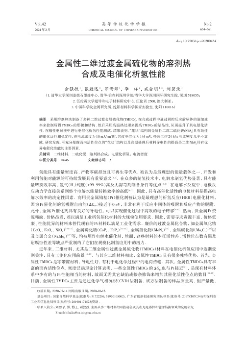
Vol.42 2021年2月No.2654~661 CHEMICAL JOURNAL OF CHINESE UNIVERSITIES高等学校化学学报金属性二维过渡金属硫化物的溶剂热合成及电催化析氢性能余强敏1,张致远1,罗雨婷1,李洋2,成会明1,3,刘碧录1(1.清华大学深圳盖姆石墨烯中心,清华⁃伯克利深圳学院/清华大学深圳国际研究生院,深圳518055;2.伍伦贡大学超导和电子材料研究中心,伍伦贡2500,澳大利亚;3.中国科学院金属研究所,沈阳材料科学国家实验室,沈阳110016)摘要采用溶剂热法制备了多种二维过渡金属硫化物(TMDCs),在合成过程中通过调控反应前驱体的滴加速率来控制所得TMDCs的形貌和结构.然后采用高温热处理来提高TMDCs的结晶性,从而提升了其电催化活性.在酸性电解液中进行电催化析氢性能测试.结果表明,“花状”结构的金属性二维二硫化铌(NbS2)具有最佳的催化活性和稳定性,在电流密度为10mA/cm2时,其过电位仅为146mV,持续工作24h后电流密度几乎不衰减.研究发现,可充分暴露面内活性位点的“花状”结构以及高温处理后材料导电性的提高是二维NbS2具有优异电催化性能的主要因素.关键词二维材料;二硫化铌;溶剂热合成;电催化析氢;电流密度中图分类号O646文献标志码A氢能具有能量密度高、产物零碳排放且可再生等优点,被认为是最理想的能量载体之一,开发和利用氢能对能源的可持续发展具有重要意义[1,2].在众多的制氢技术中,电解水制氢优势显著,具有能量转换效率高、氢气(H2)纯度(>99.99%)高及无需苛刻制备条件等优点[3~5].在电解水反应中,电极反应动力学直接关系到整个电解水能量转换效率的高低[6,7].因此,具有高催化活性的电极材料是提高电解水效率的决定性因素.商用贵金属铂基(Pt)催化剂被认为是最理想的析氢反应(HER)电催化材料,因为Pt催化剂的氢吸附自由能(ΔG H*)接近于0eV,非常有利于反应中间体的吸附和反应产物的脱附.此外,金属Pt催化剂具有良好的导电性,可以实现催化过程中高效的电子转移[8,9].然而,贵金属Pt资源稀缺、价格昂贵,难以满足工业析氢催化材料的大规模使用要求.因此,需要寻求资源丰富、价格低廉、性能优异的材料来替代现有的Pt材料以满足工业化需求.廉价的过渡金属化合物,如金属氧化物(CoO x,FeO x,NiO x)[10,11]、金属磷化物(CoP x,FeP x)[12~14]、金属氮化物(MoN x)[15]、金属碳化物(Mo x C y)[16]以及金属合金(Ni x Mo y)[17]等,均被用作电解水催化剂,然而,这些材料的本征活性差、活性位点数有限及耐腐蚀性差等缺点严重制约了它们在规模化制氢应用中的潜力.近年来,二维材料,尤其是二维金属性过渡金属硫化物(TMDCs)材料在电催化析氢应用中逐渐受到关注,具有工业化应用前景[18~20].与其它二维材料相比,金属性TMDCs具有很多独特优势.首先,金属性TMDCs是零带隙材料,导电性好,有利于电化学过程中的电荷传输.其次,金属性TMDCs具有丰富的面内活性位点,密度泛函理论计算表明,一些金属性TMDCs的ΔG H*也与Pt接近[21],是现有材料体系中少有的与Pt性能相当的材料,故而无需其它缺陷或掺杂修饰来增加其催化活性位点的数目[22~25].目前,金属性TMDCs主要是通过化学气相沉积(CVD)法制备,该方法制备的样品质量高,但产量低,doi:10.7503/cjcu20200454收稿日期:2020-07-14.网络出版日期:2020-10-13.基金项目:国家自然科学基金(批准号:51722206,51920105002)、广东省创新创业研究团队项目(批准号:2017ZT07C341)和深圳市工业和信息化局项目(批准号:201901171523)资助.联系人简介:刘碧录,男,博士,副教授,主要从事二维材料的可控制备及其在光电器件和能源转换领域的应用研究.E-mail:********************655 No.2余强敏等:金属性二维过渡金属硫化物的溶剂热合成及电催化析氢性能因而难以在电催化剂中获得规模化应用.相比于CVD法,液相法合成通常具备规模化制备的优点,是可大量制备金属性TMDCs的潜在重要方法.本文采用溶剂热法制备不同导电属性的TMDCs催化剂.以金属性NbS2为主要研究对象,研究了反应前驱体的滴加速率对催化剂形貌结构的影响和高温退火处理对催化剂结晶性的影响,考察了其在酸性条件下的电催化析氢活性及稳定性,为金属性TMDCs在高效电解水制氢中的应用提供了新思路.1实验部分1.1试剂与仪器五氯化铌(NbCl5,纯度99.5%)、五氯化钼(MoCl5,纯度99.5%)、三氯化钒(VCl3,纯度99.5%)、十二硫醇(DDT,纯度99.0%)和油胺(OLA,纯度85.0%)均购于上海阿拉丁生化科技股份有限公司;硫酸(H2SO4,质量分数98.0%)、丙酮(C3H6O,纯度99.5%)和乙醇(C2H6O,纯度99.8%)均购于国药集团化学试剂有限公司.SU-8010型场发射扫描电子显微镜(SEM,日本日立公司);Tecnai F30型透射电子显微镜(TEM,美国FEI公司);PHI5000VersaProbeII型X射线光电子能谱仪(XPS,日本Ulvac公司);D8Advance型X射线衍射仪(XRD,德国布鲁克公司);LabRAM HR型拉曼光谱仪(Raman,激发波长532nm,日本Horiba 公司);VMP-300型电化学工作站(法国Biologic公司).1.2实验过程不同导电属性的二维TMDCs电催化剂通过溶剂热法和高温热处理制备.首先,将25g油胺和138 mg NbCl5依次加入到100mL的圆底烧瓶中,向圆底烧瓶中的油胺通入氮气(流量为30sccm)直至反应结束,使得NbCl5处于氮气环境下避免空气进入,在此过程中通过施加搅拌使NbCl5均匀分散在油胺溶液中.然后将装有油胺溶液的圆底烧瓶加热至280℃恒温后,以不同速度(5.0,1.0,0.2和0.1mL/min)滴加3.0mL DDT,继续反应1h后冷却至室温,加入过量的丙酮洗涤产物,通过离心分离作用洗涤固体样品(重复3次).样品再次用乙醇和去离子水依次清洗并真空干燥烘干.最后将干燥的样品置于管式炉中在不同温度(650,750和850℃)下退火处理2h,退火升温速率为10℃/min,退火过程中通入氩氢混合气(95sccm Ar+5sccm H2);退火处理后冷却至室温取最终产物(NbS2)待用.在相同条件下分别合成出NbS2、二硫化钼(MoS2)和二硫化钒(VS2)3种二维材料.此外,采用相同制备过程将NbS2生长在钼箔(Mo foil)上用作自支撑电极,在样品洗涤过程中,将NbS2/Mo foil浸泡在丙酮和乙醇中12h后烘干,最后将烘干的样品置于管式炉中,在750℃下通入氩氢混合气(95sccm Ar+5sccm H2)退火处理2h,然后冷却至室温获得最终产物(NbS2/Mo foil).1.3电化学析氢性能测试不同电催化剂的催化性能在室温下采用标准三电极体系进行测试.其中将TMDC催化剂(负载量约为0.3mg/cm2)负载在玻碳电极上作为工作电极,石墨棒为对电极,饱和银/氯化银为参比电极,0.5 mol/L H2SO4溶液为电解液.向电解液中通30min氮气(流量为50sccm),以排除溶液中的其它气体.线性扫描伏安曲线(LSV)的工作电压为0.1~‒0.5V,扫描速率为5mV/s;电化学阻抗谱(EIS)的电压设为‒0.2V,交流频率范围为0.1~105Hz,振幅为5mV;循环伏安(CV)曲线以不同扫描速率在相对标准氢电极电位为0.05~0.15V范围内进行测试;电化学活性面积(ECSA)通过不同扫描速率(10,20,40,60和80mV/s)下的循环伏安曲线转化得到.采用恒电位法在不同电位下进行长时稳定性(I-t)测试.电化学电位(E)均根据可逆氢电极进行校正(V vs.RHE),在0.5mol/L H2SO4溶液中,E(RHE)=E(Ag/AgCl)+0.20V. 2结果与讨论2.1催化剂的形貌与结构表征在退火温度为750℃下,不同DDT滴加速率下合成的NbS2如图1所示.由图1(A~D)可见,随着DDT滴加速率的减小,NbS2逐渐由微米颗粒转变为片层结构,最终呈现出二维纳米片组成的“花状”形Vol.42高等学校化学学报貌.DDT 作为反应还原剂,其滴加速率直接影响到NbS 2成核的快慢.当DDT 大量滴加(滴加速率快)时,由于反应速率过快,形成的晶核因高的表面能导致其相互聚集而形成块体结构.将DDT 滴加速率减慢,成核反应速率也相应变慢,团聚现象逐渐减弱,从而更易形成二维纳米片状晶体结构.采用电化学循环伏安法对以上4种不同DDT 滴加速率条件合成的NbS 2材料的电化学活性面积进行了测试(图S1,见本文支持信息).图1(E )给出了4种NbS 2电催化剂的充放电电流差(ΔJ )与扫描速率的线性关系,根据公式换算后所得的催化剂电化学活性面积如图1(F )所示.当DDT 滴加速率为5.0mL/min 时,其电化学活性面积仅为20.2cm 2,随着DDT 滴加速率逐渐减至0.1mL/min 时,其电化学活性面积增大至159.5cm 2,展现出二维材料的高比表面积特征,有利于电催化反应过程中的反应前驱体与催化位点充分接触,图1(G )所示为二维NbS 2材料及其HER 过程示意图.进一步对具有高比表面积的NbS 2材料(DDT 滴加速率为0.1mL/min ,退火温度为750℃下合成)进行元素分析及晶体结构和原子结构的表征.图S2(见本文支持信息)为NbS 2材料的EDS 元素成分分布图及相应的谱线,测试结果显示材料成分中S/Nb 的原子比为1.93∶1,与理论值2∶1相近.图2(A )为NbS 2材料的XRD 谱图,4个强衍射峰对应于NbS 2的(002),(100),(110)和(200)晶面,与NbS 2标准卡片(PDF#41-0980)的衍射峰一致[26,27],表明所制备的NbS 2是2H 相晶体结构.图2(B )为NbS 2材料的Raman 光谱图,3个Raman 特征峰(E 1g ,278cm -1;E 2g ,330cm -1;A 1g ,382cm -1)与文献[28]报道的2H 相NbS 2材料一致,与XRD 所得的结构相吻合.为进一步确定合成产物的价态,采用XPS 测定了NbS 2的Nb 和S 元素的结合能,结果如图S3(见本文支持信息)和图2(C ,D )所示.首先,由图S3可见,合成的样品中仅含有Nb ,S ,C 和O 4种元素.图2(C )中Nb 3d 谱图存在3组峰,分别对应于Nb 5+(210.5eV )、Nb 4+(3d 3/2,207.7eV ;3d 5/2,204.3eV )以及阴离子插层Nb (4‒δ)+(3d 3/2,206.5eV ;3d 5/2,203.7eV )[27];图2(D )S 2p 谱图的2组峰分别对应于S —O(164.7eV )和S 2‒(2p 1/2,163.3eV ;2p 3/2,162.0eV [29]).以上结果表明,溶剂热合成的主要产物是NbS 2材料.对产物进行TEM 表征,如图2(E )所示,NbS 2呈现二维层状结构;高分辨透射电子显微镜(HRTEM )照片显示NbS 2材料具有高质量晶态结构[图2(F )],晶格间距为0.30nm ,对应于2H 相NbS 2的(100)晶面.此外,对其它2种溶剂热合成的MoS 2和VS 2材料也进行了HRTEM 表征,均呈现出高质量的晶体结构(图S4,见本文支持信息).以上结果表明,溶剂热法及后续Fig.1SEM images of two⁃dimensional(2D)NbS 2with different injecting rates of DDT precursors(A —D),capacitive currents at the potential of 0.10V against the scan rate calculated from Fig.S1(E),ECSAof NbS 2samples with different injecting rates of DDT precursors(F)and schematic of 2D NbS 2forHER(G)Injecting rate of DDT/(mL ·min -1):(A)5.0;(B)1.0;(C)0.2;(D)0.1.656No.2余强敏等:金属性二维过渡金属硫化物的溶剂热合成及电催化析氢性能高温处理对合成高质量的2H 相TMDCs 晶体具有普适性.2.2电化学析氢性能为评价不同条件下合成的二维NbS 2材料的电催化析氢性能,测试了其催化活性和动力学特性,结果见图3.图3(A )为DDT 滴加速率为0.1mL/min 时不同退火温度处理的NbS 2的线性扫描伏安曲线.与未经退火处理的材料相比,退火处理后的NbS 2材料的催化活性大幅提高;在退火处理温度为750℃时性能达到最佳,该样品在电流密度为10mA/cm 2时过电位仅为146mV ,远小于同等条件下未经退火处Fig.2XRD pattern(A),Raman spectrum(B),XPS spectra of Nb 3d (C)and S 2p (D),TEM(E)and HRTEM(F)images of metallic 2D NbS 2materialsFig.3LSV curves(A)and corresponding Tafel curves(B)of NbS 2with different annealing temperatures,LSV curves(C)of NbS 2with different injecting rates of DDT precursors and overpotentials(D)ofNbS 2at 10and 50mA/cm 2under different injecting rates of DDT precursors657Vol.42高等学校化学学报理的样品(在10mA/cm2时过电位为305mV).当退火温度高于或低于750℃时,样品的催化活性均减弱.进一步评价了不同退火温度处理的NbS2电催化剂在HER中的动力学特性,如图3(B)所示.根据塔菲尔方程η=a+b lg J[其中,a(mV)为电流密度为单位数值(1mA/cm2)时的过电位值;J(mA/cm2)为电流密度;b(mV/dec)为塔菲尔常数,b值越小,催化剂活性越高]计算了其在HER过程的塔菲尔斜率.在电催化析氢过程中,750℃退火处理后的NbS2催化剂的塔菲尔斜率为45mV/dec,远小于未经退火处理的NbS2材料的116mV/dec,表明750℃退火处理的NbS2表现出优异的动力学特性.此外,对不同退火温度处理的NbS2电催化剂的电荷传输能力进行评价,结果如图S5(见本文支持信息)所示,可见,750℃退火条件下NbS2的电荷传输电阻约为30Ω,小于850℃的35Ω,远小于650℃的63Ω和未退火样品的106Ω,表明750℃退火条件下的NbS2具有更快的电子转移速率.根据以上结果可知,高温退火处理可提升材料的导电性和结晶度,提高材料的催化活性.相反,过高温度的还原气氛处理不利于保持材料原始的本征结构,如图S6(见本文支持信息)所示,与750℃下退火后的NbS2样品相比,850℃退火后的样品其Nb3d峰整体向低结合能方向偏移约1.0eV,表明NbS2中的Nb从本征的+4价态转变为更低价态,从而改变了NbS2的本征结构;另外,金属性NbS2本征结构的改变使得NbS2的导电性降低,进而使其催化活性降低.除了退火条件,对不同DDT滴加速率下制备的NbS2的析氢催化活性进行了电催化性能表征,其具体变化趋势如图3(C)所示.随着DDT滴加速率的减小,NbS2的催化活性逐渐提高,原因在于:一方面滴加速率慢有利于二维薄层结构的形成,从而暴露更多催化活性位点;另一方面,“花状”多孔结构的形成有利于反应中质子的传输及气体扩散,可进一步提高HER速率.此外,由图3(D)可见,当电流密度从10mA/cm2增加到50mA/cm2时,“花状”多孔结构NbS2所需电位只增加了102mV,远小于微米颗粒NbS2的140mV,进一步表明“花状”多孔结构NbS2具有更快的HER反应动力学.基于以上研究结果,通过优化实验参数制备了不同种类的TMDCs材料,包括金属性的二维NbS2和VS2,以及半导体性的二维MoS2.对优化后的3种不同TMDCs进行了HER电催化活性表征.如图4(A )Fig.4LSV curves(A)and corresponding Tafel curves(B)of MoS2,VS2,NbS2and Pt/C catalysts,EIS curvesof MoS2,VS2and NbS2catalysts(C)and the stability curve of NbS2catalysts at the potential of-0.146V(vs.RHE)(D)The inset of(C)is the equivalent circuit used to fit the impedance spectra.The inset of(D)is the LSV curves of NbS2 catalyst before and after5000cycles of CV scans from‒0.3V to0.1V(vs.RHE).658No.2余强敏等:金属性二维过渡金属硫化物的溶剂热合成及电催化析氢性能所示,在电流密度10mA/cm 2下,NbS 2、VS 2和MoS 2的过电位分别为145,148和201mV ,表明金属性TMDCs 具有更高的反应活性,与文献报道一致[21];图4(B )为NbS 2、VS 2和MoS 23种催化剂的塔菲尔曲线,其斜率分别为45,50和63mV/dec ,说明3种不同TMDCs 催化剂的HER 过程均遵循Volmer -Heyrovsky 的反应机理[30].图4(C )为3种TMDCs 催化剂的Nyquist 图,图中半圆直径表示电极电荷转过移电阻R ct ,插图为实际测试电化学阻抗的拟合模型.测试结果显示,NbS 2和VS 2的R ct 分别为30和32Ω,远低于MoS 2的64Ω,表明金属性TMDCs 催化剂具有良好的电子传输能力和HER 动力学.除电催化活性外,电极材料的稳定性和耐久性也是评价电催化剂实际应用价值的重要依据.图4(D )为NbS 2催化剂的稳定性和耐久性测试曲线,在恒电压下连续工作24h 后,NbS 2催化剂的电流密度几乎未衰减.此外,在循环5000次后,NbS 2催化剂在10mA/cm 2电流密度下所需过电位基本没有增大.对电化学循环后的NbS 2催化剂进行形貌结构表征,如图S7(见本文支持信息)所示,样品在经过电化学循环后无明显团聚现象,其晶格结构无明显变化,该结果表明NbS 2催化剂具有良好的电化学稳定性.以上结果均表明,相较于半导体性TMDCs ,金属性TMDCs 在HER 中具有更高的催化活性和应用前景.为进一步验证溶剂热法制备的金属性TMDCs 在实际析氢反应中的应用前景,将生长在钼箔基底上的NbS 2(NbS 2/Mo foil)自支撑电极置于高电流密度析氢条件下进行测试,结果如图5(A )所示.在400mA/cm 2的高电流密度下,NbS 2/Mo foil 所需过电位仅为386mV ,略高于同等条件下Pt 催化剂的303mV.为验证制备的NbS 2/Mo foil 自支撑电极的稳定性,对其进行了长时间计时电流测试.如图5(B )所示,在过电位为225mV 下持续工作24h ,NbS 2/Mo foil 的电流衰减率仅为0.1mA/h ,该结果证明NbS 2/Mo foil 自支撑电极具有良好的电化学稳定性.催化材料的规模化制备是衡量其工业应用中的重要指标[31,32],基于此,不同催化剂制备方法的产能需进一步评价.目前制备金属性TMDCs的方法包括CVD 法、溶剂热法和化学气相输运(CVT )法.不同方法制备的金属性TMDCs展现出不同的析氢活性,如图6和表1所示,在电流密度为10mA/cm 2时,CVD 法和溶剂热法制备的金属性TMDCs 在电流密度为10mA/cm 2下的析氢过电位均小于200mV ,优于同等条件下CVT 法制备样品的过电位(300~1000mV ).从表1可见,CVT 和溶剂热法制备的金属性TMDCs 可实现10~100mg/h的生产速率,高出CVD 法2~3个数量级.综上,溶剂热法是规模化制备高性能金属性TMDCs 电催化剂的最佳方法,具有潜在的工业化应用前景.Fig.5LSV curves(A)and I ⁃t curve(B)of self⁃supporting electrode of NbS 2/MofoilFig.6Performance and production rate of diffe -rent TMDCs by CVT,CVD and solvother⁃mal methods 659Vol.42高等学校化学学报3结论采用溶剂热法制备出不同导电属性的TMDCs 析氢电催化剂.通过调控DDT 反应前驱体的滴加速率和产物高温退火处理,可显著提高NbS 2的催化性能.酸性电解质中,当电流密度为10mA/cm 2时,NbS 2所需的析氢过电位仅为146mV ;动力学分析发现,该类催化剂遵循Volmer -Heyrovsky 反应机理.通过对比TMDCs 材料的3种主要合成方法,发现溶剂热法制备的TMDCs 与CVD 法制备的材料催化性能相当,并远优于CVT 法制备的TMDCs 材料.值得指出的是,溶剂热法制备TMDC 的产率比CVD 法高2~3个数量级.表明溶剂热法制备的TMDC 电催化剂在实际电解水析氢技术中具有良好的应用前景.支持信息见/CN/10.7503/cjcu20200454.参考文献[1]Schloegl R.,Nat.Mater .,2008,7(10),772—774[2]Dresselhaus M.S.,Thomas I.L.,Nature ,2001,414(6861),332—337[3]Turner J.A.,Science ,2004,305(5686),572—574[4]Holladay J.D.,Hu J.,King D.L.,Wang Y.,Catalysis Today ,2009,139(4),244—260[5]Kibler L.A.,Chemphyschem ,2006,7(5),985—991[6]Seh Z.W.,Kibsgaard J.,Dickens C.F.,Chorkendorff I.,Norskov J.K.,Jaramillo T.F.,Science ,2017,355(6321),4998[7]Khan M.A.,Zhao H.,Zou W.,Chen Z.,Cao W.,Fang J.,Xu J.,Zhang L.,Zhang J.,Electrochemical Energy Reviews ,2018,1,483—530[8]Yu Q.,Luo Y.,Mahmood A.,Liu B.,Cheng H.M.,Electrochemical Energy Reviews ,2019,2,373—394[9]Yu W.T.,Porosoff M.D.,Chen J.G.,Chem.Rev.,2012,112(11),5780—5817[10]Yin H.J.,Tang Z.Y.,Chem.Soc.Rev.,2016,45(18),4873—4891[11]Han L.,Dong S.J.,Wang E.K.,Advanced Materials ,2016,28(42),9266—9291[12]Wang Y.,Kong B.,Zhao D.Y.,Wang H.T.,Selomulya C.,Nano Today ,2017,15,26—55[13]Wang C.F.,Xu Q.Y.Wang L.C.,Zhang R.Q.,Pan X.X.,Wang J.W.,Hao W.J.,Chem.J.Chinese Universities ,2019,40(10),2156—2163(王晨峰,徐秋雨,王临才,张瑞琦,潘欣欣,王景伟,郝伟举.高等学校化学学报,2019,40(10),2156—2163)[14]Wang W.F.,Qin S.,Zhang R.R.,Zhou P.P.,Yang Q.H.,Chen T.Y.,Chem.J.Chinese Universities ,2019,40(9),1979—1987(王文峰,秦山,张荣荣,周盼盼,杨庆华,陈天云.高等学校化学学报,2019,40(9),1979—1987)[15]Jin H.,Liu X.,Vasileff A.,Jiao Y.,Zhao Y.,Zheng Y.,Qiao S.Z.,ACS Nano ,2018,12(12),12761—12769[16]Zhang C.,Luo Y.T.,Tan J.Y.,Yu Q.M.,Yang F.N.,Zhang Z.Y.,Yang L.S.,Cheng H.M.,Liu B.L.,Nature Commun.,2020,11,3724[17]Zhou Q.,Li Z.Y.,Wang F.,Chem.J.Chinese Universities ,2019,40(8),1717—1725(周琦,李志洋,汪帆.高等学校化学学报,2019,40(8),1717—1725)[18]Yan Y.,Xia B.Y.,Xu Z.C.,Wang X.,ACS Catalysis ,2014,4(6),1693—1705[19]Zhang G.,Liu H.J.,Qu J.H.,Li J.H.,Energy &Environmental Science ,2016,9(4),1190—1209[20]Li H.Y.,Jia X.F.,Zhang Q.,Wang X.,Chem.,2018,4(7),1510—1537Table 1Summary of synthesis methods,sample description and overpotentials of TMDCs for HER Sample MX 2(M =V ,Nb ,Ta ;X=S ,Se ,Te )TaS 21T⁃TaS 22H⁃TaS 22H⁃TaS 22H⁃TaS 2NbS 21T⁃TaS 22H⁃NbS 22H⁃MoS 22H⁃NbS 22H⁃VS 22H⁃MoS 2Synthesis method CVT CVT CVT CVT CVD CVD CVD CVD Solvothermal Solvothermal SolvothermalMorphologic structure Hexagon Nanosheets HexagonHexagon Hexagon Nanoflakes Hexagon Hexagon Flower⁃like Flower⁃likeFlower⁃like Overpotential/V at 10mA/cm 20.60―1.000.300.801.000.550.06―0.160.160.2050.0500.0870.1460.1480.201Production rate/(mg·h -1)ca .102101―102101―102101―10210-3―10-110-3―10-110-3―10-110-3―10-1101―102101―102101―102Ref.[33][34][35][36][24][37][38][22][39]This work This work 660No.2余强敏等:金属性二维过渡金属硫化物的溶剂热合成及电催化析氢性能[21]Tsai C.,Chan K.,Nørskov J.K.,Abild⁃Pedersen F.,Surface Science,2015,640,133—140[22]Liu Y.,Wu J.,Hackenberg K.P.,Zhang J.,Wang Y.M.,Yang Y.,Keyshar K.,Gu J.,Ogitsu T.,Vajtai R.,Lou J.,Ajayan P.M.,Wood Brandon C.,Yakobson B.I.,Nature Energy,2017,2(9),17127[23]Zhang J.,Wu J.J.,Zou X.L.,Hackenberg K.,Zhou W.,Chen W.B.,Yuan J.T.,Keyshar K.,Gupta G.,Mohite A.,Ajayan P.M.,Lou J.,Mater.Today,2019,25,28—34[24]Shi J.,Wang X.,Zhang S.,Xiao L.,Huan Y.,Gong Y.,Zhang Z.,Li Y.,Zhou X.,Hong M.,Fang Q.,Zhang Q.,Liu X.,Gu L.,Liu Z.,Zhang Y.,Nature Commun.,2017,8(1),958[25]Yu Q.,Luo Y.,Qiu S.,Li Q.,Cai Z.,Zhang Z.,Liu J.,Sun C.,Liu B.,ACS Nano,2019,13(10),11874—11881[26]Han J.H.,Kim H.K.,Baek B.,Han J.,Ahn H.S.,Baik M.H.,Cheon J.,J.Am.Chem.Soc.,2018,140(42),13663—13671[27]Zhang J.,Du C.,Dai Z.,Chen W.,Zheng Y.,Li B.,Zong Y.,Wang X.,Zhu J.,Yan Q.,ACS Nano,2017,11(10),10599—10607[28]Mcmullan W.G.,Irwin J.C.,Solid State Commun.,1983,45(7),557—560[29]Ou X.,Xiong X.H.,Zheng F.H.,Yang C.H.,Lin Z.H.,Hu R.Z.,Jin C.,Chen Y.,Liu M.L.,J.Power Sources,2016,325,410—416[30]Wang J.,Xu F.,Jin H.Y.,Chen Y.Q.,Wang Y.,Adv.Mater.,2017,29(14),1605838[31]Zhang C.,Tan J.,Pan Y.,Cai X.,Zou X.,Cheng H.M.,Liu B.,National Sci.Rev.,2020,7(2),324—332[32]Yang L.,Chen W.,Yu Q.,Liu B.,Nano Research,2020,/10.1007/s12274⁃020⁃2897⁃3[33]Chia X.,Ambrosi A.,Lazar P.,Sofer Z.,Pumera M.,J.Mater.Chem.A,2016,4(37),14241—14253[34]Nguyen T.P.,Choi S.,Jeon J.M.,Kwon K.C.,Jang H.W.,Kim S.Y.,J.Phys.Chem.C,2016,120(7),3929—3935[35]Luxa J.,Mazanek V.,Pumera M.,Lazar P.,Sedmidubsky D.,Callisti M.,Polcar T.,Sofer Z.,Chem.,2017,23(33),8082—8091[36]Feng Y.,Gong S.J.,Du E.W.,Chen X.F.,Qi R.J.,Yu K.,Zhu Z.Q.,J.Phys.Chem.C,2018,122(4),2382—2390[37]Zhou X.F.,Lin S.H.,Yang X.L.,Li H.N.,Hedhili M.N.,Li L.J.,Zhang W.J.,Shi Y.M.,Nanoscale,2018,10(7),3444—3450[38]Huan Y.,Shi J.,Zou X.,Gong Y.,Zhang Z.,Li M.,Zhao L.,Xu R.,Jiang S.,Zhou X.,Hong M.,Xie C.,Li H.,Lang X.,Zhang Q.,Gu L.,Yan X.,Zhang Y.,Advanced Materials,2018,30(15),e1705916[39]Luo Y.,Tang L.,Khan U.,Yu Q.,Cheng H.M.,Zou X.,Liu B.,Nature Commun.,2019,10(1),269Solvothermal Synthesis of2D Metallic Transition Metal Disulfides forEfficient Electrocatalytic Hydrogen Evolution†YU Qiangmin1,ZHANG Zhiyuan1,LUO Yuting1,LI Yang2,CHENG Huiming1,3,LIU Bilu1*(1.Shenzhen Geim Graphene Center,Tsinghua⁃Berkeley Shenzhen Institute&Tsinghua Shenzhen InternationalGraduate School,Tsinghua University,Shenzhen518055,China;2.Institute for Superconducting and Electronic Materials,University of Wollongong,Wollongong2500,Australia;3.Shenyang National Laboratory for Materials Sciences,Institute of Metal Research,Chinese Academy of Sciences,Shenyang110016,China)Abstract Different kinds of transition metal disulfides(TMDCs)were prepared via solvothermal method.The morphologic structure of TMDCs were controlled by tuning the injecting rates of the reaction precursor.The crystallization of the products could be improved by annealing treatment at high-temperature,and thus impro-ving the electrocatalytic activity of TMDC catalyst.The results of electrocatalytic hydrogen evolution in acidic electrolyte show that the metallic"flower-like"niobium disulfide(NbS2)exhibits excellent catalytic activity and stability.It possess a small overpotential of only146mV to achieve a current density of10mA/cm2.The current density almost shows no decays after24h continuous working at10mA/cm2.The excellent perfor⁃mance of NbS2catalyst is attributed to the"flower-like"structure that can expose abundant active sites,and to the improvement of electrical conductivity and material quality after annealing treatment.Keywords2D Material;NbS2;Solvothermal synthesis;Electrocatalytic hydrogen evolution;Currentdensity(Ed.:Y,K,S)Science Foundation of China(Nos.51722206,51920105002),the Program of Guangdong Innovative(No.2017ZT07C341)and the Program of Bureau of Industry and Information Technology of Shen⁃zhen,China(No.201901171523).661。
xrd实验报告中南
中南大学X射线衍射实验报告材料科学与工程学院材料科学与工程专业1604 班级姓名任稳学号0603160409 同组者实验日期2018 年11 月11 日指导教师黄继武评分分评阅人评阅日期一、实验目的1)掌握X射线衍射仪的工作原理、操作方法;2)掌握X射线衍射实验的样品制备方法;3)学会X射线衍射实验方法、实验参数设置,独立完成一个衍射实验测试;4)学会MDI Jade 6的基本操作方法;5)学会物相定性分析的原理和利用Jade进行物相鉴定的方法;6)学会物相定量分析的原理和利用Jade进行物相定量的方法。
本实验由衍射仪操作、物相定性分析、物相定量分析三个独立的实验组成,实验报告包含以上三个实验内容。
二、实验原理1、X射线衍射仪(1)X射线管X射线管工作时阴极接负高压,阳极接地。
灯丝附近装有控制栅,使灯丝发出的热电子在电场的作用下聚焦轰击到靶面上。
阳极靶面上受电子束轰击的焦点便成为X 射线源,向四周发射X 射线。
在阳极一端的金属管壁上一般开有四个射线出射窗口。
转靶X 射线管采用机械泵+分子泵二级真空泵系统保持管内真空度,阳极以极快的速度转动,使电子轰击面不断改变,即不断改变发热点,从而达到提高功率的目的(2)测角仪系统测角仪圆中心是样品台,样品台可以绕中心轴转动,平板状粉末多晶样品安放在样品台上,样品台可围绕垂直于图面的中心轴旋转;测角仪圆周上安装有X 射线辐射探测器,探测器亦可以绕中心轴线转动;工作时,一般情况下试样台与探测器保持固定的转动关系(即θ-2θ连动),在特殊情况下也可分别转动;有的仪器中样品台不动,而X 射线发生器与探测器连动。
(3)衍射光路2、物相定性分析1) 每一物相具有其特有的特征衍射谱,没有任何两种物相的衍射谱是完全相同的2) 记录已知物相的衍射谱,并保存为PDF 文件3) 从PDF 文件中检索出与样品衍射谱完全相同的物相4) 多相样品的衍射谱是其中各相的衍射谱的简单叠加,互不干扰,检索程序能从PDF 文件中检索出全部物相3、物相定量分析物相定量分析——绝热法在一个含有N 个物相的多相体系中,每一个相的RIR 值(参比强度)均为已知的情况下,测量出每一个相的衍射强度,可计算出其中所有相的质量分数:其中某相X 的质量分数可表示为:∑==N A i iA i X A XX K I K I W式中A 表示N 个相中被选定为内标相的物相名称直至全部物相鉴定出来。
中科大晶体学与材料结构表征第1次作业参考答案

MSEN6414PHomework IDue Nov. 30, 20201.Look for the structures of the following molecules in the Internet. Assign the pointgroups for them (5 points each).molecular structure2. Consider just two-dimensional space for this problem. Calculate the basis vectors of the reciprocal lattice for a centered rectangular lattice with basis vectors of its conventional unit cell a = 6.06 Å, b =3.50 Å (15 points). Draw the Wigner-Seitz cell for the reciprocal lattice and calculate its area in Å-2 (10 points). What rotational symmetry does this Wigner-Seitz cell resemble (5 points)? Hint: Reciprocal lattice must be calculated using the basis vectors of the primitive unit cell.Solution:121111222122 basis vectors are:Let the basis vectors of the reciprocal lattice be:As shown in the figure, ,22 22From 2 ,w i j ij a b a i j a ba i jb b i b j b b i b ja b πδ=+=-+=+=+=12 e can get that 2222is shown on the right:And the basis vectors of the reciprocal lattice are:The Wigner-Seitz cell for the reciprocal latt its ice a b i j a b b i ja bππππ=+=-+ 16 222220This Wigner-S rea:eitz cell resembles rotational s 888 3.72A6.06 3.5ymmetry.0S b b C k ab ab πππ-=⨯====⨯3. For the space group C2/m , provide the point group (10 points), the set of essential symmetry operations (10 points), and the coordinates for all the general positions in the conventional unit cell (20 points). Please select the unit cell axes in such a way that β ≠ 90︒. Hint: C-centering will also contribute to the multiplicity of general positions. Solution:the point group: 2/msymmetry operations: 1 2 m 1the coordinates for all the general positions in the conventional unit cell:110,,22⎛⎫ ⎪⎝⎭, 10,0,2⎛⎫ ⎪⎝⎭,10,,02⎛⎫⎪⎝⎭, ()0,0,0。
英语材基试卷
英文原版教材班“材料科学基础”考试试题试卷一Examination problems of the course of “fundament of materials science”姓名:班级:记分:1. Glossary (2 points for each)1) crystal structure:2) basis (or motif):3) packing fractor:4) slip system:5) critical size:6) homogeneous nucleation:7) coherent precipitate:8) precipitation hardening:9) diffusion coefficient:10) uphill diffusion:2. Determine the indices for the planes in the cubic unit cell shown in Figure 1. (5 points)Fig. 13. Determine the crystal structure for the following: (a) a metal with a0 =4.9489 Å, r = 1.75 Å and one atom per lattice point; (b) a metal with a0 = 0.42906 nm, r = 0.1858 nm and one atom per lattice point. (10 points)4-1. What is the characteristic of brinell hardness test, rockwell hardness test and Vickers hardness test? What are the effects of strain rate and temperature on the mechanical properties of metallic materials? (15 points)4-2. What are the effects of cold-work on metallic materials? How to eliminate those effects? And what is micro-mechanism for the eliminating cold-work effects? (15 points)5-1. Based on the Pb-Sn-Bi ternary diagram as shown in Fig. 2, try to(1)Show the vertical section of 40wt.%Sn; (4 points)(2) Describe the solidification process of the alloy 2# with very low cooling speed (includingphase and microstructure changes); (4 points)(3)Plot the isothermal section at 150o C. (7 points)Fig. 25-2. A 1mm sheet of FCC iron is used to contain N2in a heated exchanger at 1200o C. The concentration of N at one surface is 0.04 atomic percent and the concentration at the second surface is 0.005 atomic percent. At 1000 o C, if same N concentration is demanded at the second surface and the flux of N becomes to half of that at 1200o C, then what is the thickness of sheet?(15 points)6-1. Supposed that a certain liquid metal is undercooled until homogeneous nucleation occurs. (15 points)(1)How to calculate the critical radius of the nucleus required? Please give the deductionprocess.(2)For the Metal Ni, the Freezing Temperature is 1453︒C, the Latent Heat of Fusion is 2756J/cm3, and the Solid-liquid Interfacial Energy is 255⨯10-7 J/cm2. Please calculate the critical radius at 1353︒C. (Assume that the liquid Ni is not solidified.)6-2. Fig.3 is a portion of the Mg-Al phase diagram. (15 points)(1)If the solidification is too rapid, please describe the solidification process of Mg-10wt%Alalloy.(2)Please describe the equilibrium solidification process of Mg-20wt%Al alloy, and calculate theamount of each phase at 300︒C.Fig. 37-1. Figure 4 shows us the Al-Cu binary diagram and some microstructures found in a cooling process for an Al-4%Cu alloy. Please answer following questions according to this figure. (20 points)Fig. 4(1)What are precipitate, matrix and microconstituent? Please point them out in the in the figure and explain.(2)Why is need-like precipitate not good for dispersion strengthening? The typical microstructure shown in the figure is good or not? why?(3)Please tell us how to obtain the ideal microstructure shown in this figure.(4)Can dispersion strengthened materials be used at high temperature? Please give the reasons (comparing with cold working strengthening)7-2. Please answer following questions according to the time-temperature-transformation (TTT) diagram as shown in Fig. 5. (20 points)(1)What steel is this TTT diagram for? And what means P, B, and M in the figure? (2)Why dose the TTT diagram exhibi ts a ‘C’ shape?(3)Point out what microconstituent will be obtained after austenite is cooled according to the curves I, II, III and IV .(4)What is microstructural difference between the curve I and the curve II? (5)How to obtain the steel with the structure of(a) P+B(b) P+M+A (residual) (c) P+B+M+A (residual)(d) Full tempered martensiteIf you can, please draw the relative cooling curve or the flow chart of heat treatment.Fig. 5III III IV英文原版教材班“材料科学基础”考试试题答案Solution s of the course of “fundament of materials science”1. Glossary (2 points for each)1) The arrangement of the atoms in a material into a repeatable lattice.2) A group of atoms associated with a lattice.3) The fraction of space in a unit cell occupied by atoms.4) The combination of the slip plane and the slip direction.5) The minimum size that must be formed by atoms clustering together in the liquid before thesolid particle is stable and begins to grow.6) Formation of a critically sized solid from the liquid by the clustering together of a largenumber of atoms at a high undercooling (without an external interface).7) A precipitate whose crystal structure and atomic arrangement have a continuousrelationship with matrix from which precipitate is formed.8) A strengthening mechanism that relies on a sequence of solid state phase transformationsin a dispersion of ultrafine precipitates of a 2nd phase. This is same as age hardening. It is a form of dispersion strengthening.9) A temperature-dependent coefficient related to the rate at which atom, ion, or otherspecies diffusion. The DC depends on temperature, the composition and microstructure of the host material and also concentration of the diffusion species.10) A diffusion process in which species move from regions of lower concentration to that ofhigher concentration.2. Solution: A(-364), B(-340), C(346).3. Solution: (a)fcc; (b) bcc.4-1. What is the characteristic of brinell hardness test, rockwell hardness test and Vickers hardness test? What are the effects of strain rate and temperature on the mechanical properties of metallic materials? (15 points)4-2. What are the effects of cold-work on metallic materials? How to eliminate those effects? And what is micro-mechanism for the eliminating cold-work effects? (15 points)5-1. Based on the Pb-Sn-Bi ternary diagram as shown in Fig. 2, try to(1)Show the vertical section of 40wt.%Sn; (5 points)(2) Describe the solidification process of the alloy 2# with very low cooling speed (includingphase and microstructure changes); (5 points)(3)Plot the isothermal section at 150o C. (5 points)Fig. 25-2. A 1mm sheet of FCC iron is used to contain N2in a heated exchanger at 1200o C. The concentration of N at one surface is 0.04 atomic percent and the concentration at the second surface is 0.005 atomic percent. At 1000 o C, if same N concentration is demanded at the second surface and the flux of N becomes to half of that at 1200o C, then what is the thickness of sheet?(15 points)6-1. Supposed that a certain liquid metal is undercooled until homogeneous nucleation occurs. (15 points)(3)How to calculate the critical radius of the nucleus required? Please give the deductionprocess.(4)For the Metal Ni, the Freezing Temperature is 1453︒C, the Latent Heat of Fusion is 2756J/cm3, and the Solid-liquid Interfacial Energy is 255⨯10-7 J/cm2. Please calculate the critical radius at 1353︒C. (Assume that the liquid Ni is not solidified.)6-2. Fig.3 is a portion of the Mg-Al phase diagram. (15 points)(3)If the solidification is too rapid, please describe the solidification process of Mg-10wt%Alalloy.(4)Please describe the equilibrium solidification process of Mg-20wt%Al alloy, and calculate theamount of each phase at 300︒C.Fig. 37-1. Figure 4 shows us the Al-Cu binary diagram and some microstructures found in a cooling process for an Al-4%Cu alloy. Please answer following questions according to this figure. (20 points)Fig. 4(1)What are precipitate, matrix and microconstituent? Please point them out in the in the figure and explain.(2)Why is need-like precipitate not good for dispersion strengthening? The typical microstructure shown in the figure is good or not? why?(3)Please tell us how to obtain the ideal microstructure shown in this figure.(4)Can dispersion strengthened materials be used at high temperature? Please give the reasons (comparing with cold working strengthening)7-2. Please answer following questions according to the time-temperature-transformation (TTT) diagram as shown in Fig. 5. (20 points)(1)What steel is this TTT diagram for? And what means P, B, and M in the figure? (2)Why dose the TTT diagram exhibits a ‘C’ shape?(3)Point out what microconstituent will be obtained after austenite is cooled according to the curves I, II, III and IV .(4)What is microstructural difference between the curve I and the curve II? (5)How to obtain the steel with the structure of(a) P+B(b) P+M+A (residual) (c) P+B+M+A (residual)(d) Full tempered martensiteIf you can, please draw the relative cooling curve or the flow chart of heat treatment.Fig. 5III III IV英文原版教材班“材料科学基础”考试试题试卷二Examination problems of the course of “fundament of materials science”姓名:班级:记分:1. You would like to be able to physically separate different materials in a scrap recycling plant. Describe some possible methods that might be used to separate materials such as polymers, aluminum alloys, and steels from one another. (5 points)2. Plot the melting temperature of the elements in the 1A column of the periodic table versus atomic number (i.e., plot melting temperatures of Li through Cs). Discuss this relationship, based on atomic bonding and binding energy. (10 points)3.Above 882℃, titanium has a BCC crystal structure, with a = 0.332 nm. Below this temperature, titanium has a HCP structure, with a = 0.2978 nm and c = 0.4735 nm. Determine the percent volume change when BCC titanium transforms to HCP titanium. Is this a contraction or expansion? (10 points)4. The density of BCC iron is 7.882 g/cm3and the lattice parameter is 0.2866 nm whenhydrogen atoms are introduced at interstitial positions. Calculate (a) the atomic fraction of hydrogen atoms and (b) the number of unit cells required on average to contain one hydrogen atom. (15 points)5. A carburizing process is carried out on a 0.10% C steel by introducing 1.0% C at the surface at 980℃, where the iron is FCC. Calculate the carbon content at 0.01 cm, 0.05 cm, and 0.10 cm beneath the surface after 1 h. (15 points)6. The following data were collected from a standard 0.505-in.-diameter test specimen of acopper alloy (initial length (t o) = 2.0 in.):Load Gage Length Stress Strain(lb) (in.) (psi) (in/in.)0 2.00000 0 0.03,000 2.00167 15,000 0.0008356,000 2.00333 30,000 0.0016657,500 2.00417 37,500 0.0020859,000 2.0090 45,000 0.004510,500 2.040 52,500 0.0212,000 2.26 60,000 0.1312,400 2.50 (max load) 62,000 0.2511,400 3.02 (fracture) 57,000 0.51After fracture, the gage length is 3.014 in. and the diameter is 0.374 in. Plot the data and calculate (a) the 0.2% offset yield strength, (b) the tensile strength, (c) the modulus of elasticity, (d) the %Elongation, (e) the %Reduction in area, (f) the engineering stress at fracture, (g) the true stress at fracture, and (h) the modulus of resilience. (15 points)7. A 1.5-em-diameter metal bar with a 3-cm gage length is subjected to a tensile test. Thefollowing measurements are made.Change in Force (N) Gage length (cm) Diameter (cm)16,240 0.6642 1.202819,066 1.4754 1.088419,273 2.4663 0.9848Determine the strain hardening coefficient for the metal. Is the metal most likely to be FCC, BCC, or HCP? Explain.(15 points)8. Based on Hume-Rothery’s conditions, which of the following systems would be expected todisplay unlimited solid solubility? Explain. (15 points)(a) Au-Ag (b) Al-Cu (c) Al-Au (d)U-W(e) Mo-Ta (f) Nb-W (g) Mg-Zn (h) Mg-Cd英文原版教材班“材料科学基础”考试试题答案Solutions of the course of “fundament of materials science”1.Steels can be magnetically separated from the other materials; steel (or carbon-containing iron alloys) are ferromagnetic and will be attracted by magnets. Density differences could be used—polymers have a density near that of water; the specific gravity of aluminum alloys is around2.7;that of steels is between 7.5 and 8. Electrical conductivity measurements could be used—polymers are insulators, aluminum has a particularly high electrical conductivity.(5 points)2.T (o C)L i–180.7N a– 97.8K – 63.2R b– 38.9As the atomic number increases, the melting temperature decreases, (10 points)3. We can find the volume of each unit cell. Two atoms are present in both BCC and HCP titanium unit cells, so the volumes of the unit cells can be directly compared.V BCC = (0.332 nm)3 = 0.03659 nm3V HCP= (0.2978 nm)2(0.4735 nm)cos30 = 0.03637 nm3△V=x 100 =×100= -0.6%Therefore titanium contracts 0.6% during cooling. (10 points)4. (a) 7.882 g/cm3 =x = 0.0081 H atoms/cellThe total atoms per cell include 2 Fe atoms and 0.0081 H atoms. Thus:(10 points)(b) Since there is 0.0081 H/cell, then the number of cells containing H atoms is:cells = 1/0.0081 = 123.5 or 1 H in 123.5 cells (5 points)5. D = 0.23 exp[-32,900/(1.987)(1253)] = 42 × 10-8 cm2/sC x= 0.87% CC x= 0.43% CC x= 0.18% C(15 points)6. σ=FI (π/4)(0.505)2 = F/0.2ε = (l-2)/2(a) 0.2% offset yield strength = 45,000 psi(b)tensile strength = 62,000 psi(c) E = (30,000 - 0) / (0.001665 - 0) = 18 x 106 psi(d)%Elongation =(e) %Reduction in area =(f) engineering stress at fracture = 57,000 psi(g)true stress at fracture = 11,400 lb / (TC/4)(0.374)2= 103,770 psi (h) From the graph, yielding begins at about 37,500 psi. Thus:(15 points)7.Force(lb) Gage length(in.) Diameter(in.) True stress(psi) True strain(psi)16,240 3.6642 12.028 143 0.20019,066 4.4754 10.884 205 0.40019,273 5.4663 9.848 249 0.600σt=Kεt2or ln143=ln K + n ln0.2ln 249 = ln K + nln 0.6n=0.51A strain hardening coefficient of 0.51 is typical of FCC metals.(15 points)8.The Au–Ag, Mo–Ta, and Mg–Cd systems have the required radius ratio, the same crystal structures, and the same valences. Each of these might be expected to display complete solid solubility. [The Au –Ag and Mo –T a d o have isomorphous phase diagrams. In addition, the Mg–Cd alloys all solidify like isomorphous alloys; however a number of solid state phase transformations complicate the diagram.] (15 points)英文原版教材班“材料科学基础”考试试题试卷三Examination problems of the course of “fundament of materials science”姓名:班级:记分:1. You would like to be able to identify different materials without resorting to chemical analysis or lengthy testing procedures. Describe some possible testing and sorting techniques you might be able to use based on the physical properties of materials. (5 points)2. Plot the melting temperatures of elements in the 4A to 8-10 columns of the periodic table versus atomic number (i.e., plot melting temperatures of Ti through Ni, Zr through Pd, and Hf through Pt). Discuss these relationships, based on atomic bonding and binding energy, (a) as the atomic number increases in each row of the periodic table and (b) as the atomic number increases in each column of the periodic table. (10 points)3. Beryllium has a hexagonal crystal structure, with a o= 0.22858 nm and c o= 0.35842 nm. The atomic radius is 0.1143 nm, the density is 1.848 g/cm3, and the atomic weight is 9.01 g/mol. Determine (a) the number of atoms in each unit cell and (b) the packing factor in the unit cell.(10 points)4. Suppose we introduce one carbon atom for every 100 iron atoms in an interstitial position in BCC iron, giving a lattice parameter of 0.2867 nm. For the Fe-C alloy, find (a) the density and (b) the packing factor. (15 points)5. Iron containing 0.05% C is heated to 912oC in an atmosphere that produces 1.20% C at the surface and is held for 24 h. Calculate the carbon content at 0.05 cm beneath the surface if (a) the iron is BCC and (b) the iron is FCC. Explain the difference. (15 points)6. The following data were collected from a 0.4-in. diameter test specimen of poly vinyl chloride(l0 = 2.0 in):Load(lb) Gage Length(in.) Stress(psi) Strain(in/in.)0 2.00000 0 0.0300 2.00746 2,387 0.00373600 2.01496 4,773 0.00748900 2.02374 7,160 0.011871200 2.032 9,547 0.0161500 2.046 11,933 0.0231660 2.070 (max load) 13,206 0.0351600 2.094 12,729 0.0471420 2.12 (fracture) 11,297 0.06After fracture, the gage length is 2.09 in. and the diameter is 0.393 in. Plot the data and calculate (a) the 0.2% offset yield strength, (b) the tensile strength, (c) the modulus of elasticity, (d) the %Elongation, (e) the %Reduction in area, (f) the engineering stress at fracture, (g) the true stress at fracture, and (h) the modulus of resilience. (15 points)7. A titanium alloy contains a very fine dispersion of tiny Er203 particles. What will be the effectof these particles on the grain growth temperature and the size of the grains at any particular annealing temperature? Explain. (15 points)8. Suppose 1 at% of the following elements is added to copper (forming a separate alloy witheach element) without exceeding the solubility limit. Which one would be expected to give the higher strength alloy? Is any of the alloying elements expected to have unlimited solid solubility in copper?(a) Au (b) Mn (c) Sr (d) Si (e) Co (15 points)英文原版教材班“材料科学基础”考试试题答案Solutions of the course of “fundament of materials science”1.Steels can be magnetically separated from the other materials; steel (or carbon-containing iron alloys) are ferromagnetic and will be attracted by magnets. Density differences could be used—polymers have a density near that of water; the specific gravity of aluminum alloys is around2.7;that of steels is between 7.5 and 8. Electrical conductivity measurements could be used—polymers are insulators, aluminum has a particularly high electrical conductivity.(5 points)2. Ti –1668 Zr – 1852 Hf – 2227V –1900 Nb –2468 Ta – 2996Cr –1875 Mo–2610 W–3410Mn–1244 Tc –2200 Re–3180Fe –1538 Ru –2310 Os–2700Co –1495 Rh –1963 Ir –2447Ni –1453 Pd –1552 Pt –1769For each row, the melting temperature is highest when the outer “d” energy level is partly full. In Cr, there are 5 electrons in the 3d shell; in Mo, there are 5 electrons in the 4d shell; in W there are 4 electrons in the 5d shell. In each column, the melting temperature increases as the atomic number increases—the atom cores contain a larger number of tightly held electrons, making the metals more stable. (10 points)3.V= (0.22858 nm)2(0.35842 nm)cos 30 = 0.01622 nm3 = 16.22 × 10⁻²⁴ cm3(a)From the density equation:1.848 g/cm3 =x = 2 atoms/cell(b)The packing factor (PF) is:PF == 0.77 (10 points)4. There is one carbon atom per 100 iron atoms, or 1 C/50 unit cells, or 1/50 C per unit cell:(a)(b)(15 points)5. t= (24 h)(3600 s/h) = 86,400 sD BCC = 0.011 exp[-20,900/(1.9871185)] = 1.54 × 10⁻⁶ cm2/sD FCC = 0.23 exp[-32,900/(1.987)(1185)] = 1.97×10⁻⁷ cm2/sBCC: = erf[0.0685] = 0.077C x= 1.11% CFCC: = erf[0.192] = 0.2139C x = 0.95% CFaster diffusion occurs in the looser packed BCC structure, leading to the higher carbon content at point “x”. (15 points)6. σ=F /(π/4)(0.4)2 = F/0.1257ε = (l-2)/2(a)0.2% offset yield strength = 11,600 psi(b) tensile strength = 12,729 psi(c) E= (7160 - 0) / (0.01187 - 0) = 603,000 psi(d)%Elongation =(e) %Reduction in area =(f) engineering stress at fracture = 11,297 psi(g)true stress at fracture = 1420 lb / (TC/4)(0.393)2= 11,706 psi (h) From the figure, yielding begins near 9550 psi. Thus:(15 points)7. These particles, by helping pin die grain boundaries, will increase the grain growth temperature and decrease the grain size. (15 points)8.The Cu-Sr alloy would be expected to be strongest (largest size difference). The Cu-Au alloy satisfies Hume-Rothery ’s conditions and might be expected to display complete solid solubility—in fact it freezes like an isomorphous series of alloys, but a number of solid state transformations occur at lower temperatures.(15 points)英文原版教材班“材料科学基础”考试试题试卷四Examination problems of the course of “fundament of materials science”姓名:班级:记分:1.Aluminum has a density of2.7 g/cm3. Suppose you would like to produce a compositematerial based on aluminum having a density of 1.5 g/cm3. Design a material that would have this density. Would introducing beads of polyethylene, with a density of 0.95 g/cm3, into the aluminum be a likely possibility? Explain. (5 points)2. (a) Aluminum foil used for storing food weighs about 0.3 g per square inch. How many atomsof aluminum are contained in this sample of foil?(b) Using the densities and atomic weights given in Appendix A, calculate and compare thenumber of atoms per cubic centimeter in (i) lead and (ii) lithium. (10 points)3. The density of potassium, which has the BCC structure and one atom per lattice point, is0.855 g/cm3. The atomic weight of potassium is 39.09 g/mol. Calculate (a) the latticeparameter; and (b) the atomic radius of potassium. (10 points)4. The density of a sample of HCP beryllium is 1.844 g/cm3 and the lattice parameters are a0=0.22858 nm and c0= 0.35842 nm. Calculate (a) the fraction of the lattice points that containvacancies and (b) the total number of vacancies in a cubic centimeter. (15 points)5. A ceramic part made of MgO is sintered successfully at 1700℃in 90 minutes. To minimizethermal stresses during the process, we plan to reduce the temperature to 1500℃. Which will limit the rate at which sintering can be done: diffusion of magnesium ions or diffusion of oxygen ions? What time will be required at the lower temperature? (15 points)6. (a) A thermosetting polymer containing glass beads is required to deflect 0.5 mm when aforce of 500 N is applied. The polymer part is 2 cm wide, 0.5 cm thick, and 10 cm long. If the flexural modulus is 6.9 GPa, determine the minimum distance between the supports. Will the polymer fracture if its flexural strength is 85 MPa? Assume that no plastic deformation occurs.(b) The flexural modulus of alumina is 45 x 106 psi and its flexural strength is 46,000 psi. Abar of alumina 0.3 in. thick, 1.0 in. wide, and 10 in. long is placed on supports 7 in. apart.Determine the amount of deflection at the moment the bar breaks, assuming that no plastic deformation occurs. (15 points)7. Based on the following observations, construct a phase diagram. Element A melts at 850°Cand element B melts at 1200°C. Element B has a maximum solubility of 5% in element A, and element A has a maximum solubility of 15% in element B. The number of degrees of freedom from the phase rule is zero when the temperature is 725°C and there is 35% B present. At room temperature 1% B is soluble in A and 7% A is soluble in B. (15 points)8.Suppose that age hardening is possible in the Al-Mg system (see Figure 10-11). (a)Recommend an artificial age-hardening heat treatment for each of the following alloys, and(b) compare the amount of the precipitate that forms from your treatment of each alloy. (i)Al-4% Mg (ii) Al-6% Mg (iii) Al-12% Mg (c) Testing of the alloys after the heat treatment reveals that little strengthening occurs as a result of the heat treatment. Which of the requirements for age hardening is likely not satisfied? (15 points)英文原版教材班“材料科学基础”考试试题答案Solutions of the course of “fundament of materials science”1. In order to produce an aluminum-matrix composite material with a density of 1.5 g/cm 3, we wouldneed to select a material having a density considerably less than 1.5 g/cm 3. While polyethylene’s density would make it a possibility, the polyethylene has a very low melting point compared to aluminum; this would make it very difficult to introduce the polyethylene into a solid aluminum matrix —processes such as casting or powder metallurgy would destroy the polyethylene .Therefore polyethylene would NOT be a likely possibility.One approach, however, might be to introduce hollow glass beads .Although ceramic glasses have densities comparable to that of aluminum, a hollow bead will have a very low density. The glass also has a high melting temperature and could be introduced into liquid aluminum for processing as a casting. (5 points)2. (a) In a one square inch sample:number ==6.69 × 10²¹ atoms(b) (i) In lead:= 3.3 × 10²² atoms/cm 3(ii) In lithium:= 4.63 × 10²² atoms/cm 3 (10 points)3. (a) Using Equation 3-5:0.855 g/cm 3 =a o 3 = 1.5189 × 10⁻²² cm 3 or a o = 5.3355 × 10⁻⁸ cm(b) From the relationship between atomic radius and lattice parameter:r == 2.3103 × 10⁻⁸cm (10 points)4. V u.c.= (0.22858 nm)2(0.35842 nm)cos30 = 0.01622 nm 3= 1.622 x 10~23 cm 3 (a) From the density equation:x = 1.9984fraction =29984.12 = 0.0008(b) number == 0.986 x 10²⁰ vacancies/cm 3 (15 points)5. Diffusion of oxygen is the slower of the two, due to the larger ionic radius of the oxygen.D 1700= 0.000043 exp[-82,100/(1.987)(1973)] = 3.455 × 10⁻¹⁴ cm 2/sD1500= 0.000043 exp[-82,100/(1.987)(1773)] = 3.255 × 10⁻¹⁵ cm2/st1500 = D1700 t1700/D1500== 955 min = 15.9 h (15 points)6. (a) Solution:The minimum distance L between the supports can be calculated from the flexural modulus.L3 = 4w/z3δ(flexural modulus)/3FL3 = (4)(20 mm)(5 mm)3(0.5 mm)(6.9 GPA)(1000 MPa/GPa) / 500 NL3 = 69,000 mm3 or L = 41 mmThe stress acting on the bar when a deflection of 0.5 mm is obtained isσ= WL/2wh2 = (3)(500 N)(41 mm) / (2)(20 mm)(5 mm)2 = 61.5 MPaThe applied stress is less than the flexural strength of 85 MPa; the polymer is not expected to fracture.(b) Solution:The force required to break the bar isF = 2w/z2(flexural strength)/3LF= (2)(1 in)(0.3 in)2(46,000 psi / (3)(7 in.) = 394 lbThe deflection just prior to fracture is8 = FZ3/4wh3(flexural modulus)8 = (394 lb)(7 in)3/(4)(l in)(0.3 in)3(45 x 106 psi) = 0.0278 in. (15 points)7.(15 points)8. (a) The heat treatments for each alloy might be:Al-4% Mg Al-6% Mg Al-12% MgT Eutectic451°C 451°C 451°CT Solvs210°C 280°C 390°CSolutionTreat at: 210-451°C 280-451°C 390-451°CQuench Quench QuenchAge at: <210°C <280°C <390°C(b) Answers will vary depending on aging temperature selected. If all threeare aged at 200°C, as an example, the tie line goes from about 3.8 to 35% Mg:A1-4% Mg: %β = (4− 3.82)/(35 − 3.82) X 100 = 0.6%Al-6% Mg: %β = (6 − 3.82)/(35 − 3.82) X 100 = 7.1%Al-12% Mg: %β = (12 −3.82)/(35− 3.82) X 100 = 26.8%(c) Most likely, a coherent precipitate is not formed; simple dispersionstrengthening, rather than age hardening, occurs. (15 points)英文原版教材班“材料科学基础”考试试题试卷五Examination problems of the course of “fundament of materials science”姓名:班级:记分:1. You would like to design an aircraft that can be flown by human power nonstop for adistance of 30 km. What types of material properties would you recommend? What materials might be appropriate? (5 points)2. Boron has a much lower coefficient of thermal expansion than aluminum, even though bothare in the 3B column of the periodic table. Explain, based on binding energy, atomic size, and the energy well, why this difference is expected. (10 points)3. Determine the ASTM grain size number if 20 grains/square inch are observed at amagnification of 400. (10 points)4. We currently can successfully perform a carburizing heat treatment at 1200o C in 1 h. In aneffort to reduce the cost of the brick lining in our furnace, we propose to reduce the carburizing temperature to 950℃. What time will be required to give us a similar carburizing treatment? (15 points)5.The data below were obtained from a series of Charpy impact tests performed on foursteels, each having a different manganese content. Plot the data and determine (a) the transition temperature (defined by the mean of the absorbed energies in theductile and brittle regions) and (b) the transition temperature (defined as the temperature that provides 50 J absorbed energy). Plot the transition temperature versus manganese content and discuss the effect of manganese on the toughness of steel. What would be the minimum manganese allowed in the steel if a part is to be used at 0°C?Test temperature°C Impact snergy (J)0.30% Mn 0.39% Mn 1.01% Mn 1.55% Mn-100 2 5 5 15-75 2 5 7 25-50 2 12 20 45-25 10 25 40 700 30 55 75 11025 60 100 110 13550 105 125 130 14075 130 135 135 140100 130 135 135 140(15 points)。
Design of Lattice Structure for Additive Manufacturing
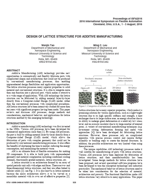
ABSTRACT Additive Manufacturing (AM) technology provides new opportunities to automatically and flexibly fabricate parts with complicated shapes and architectures that could not be produced by conventional manufacturing processes, thus enabling unprecedented design flexibilities and application opportunities. The lattice structure possesses many superior properties to solid material and conventional structures. It is able to integrate more than one function into a physical part, which makes it attractive to a wide range of applications. With AM technology the lattice structure can be fabricated by adding material layer-by-layer directly from a Computer-Aided Design (CAD) model, rather than the conventional processes with complicated procedures. AM lattice structures have been intensively studied for more than ten years with significant progress having been made. This paper reviews and discusses AM processes, design methods and considerations, mechanical behavior, and applications for lattice structures enabled by this emerging technology. INTRODUCTION Additive manufacturing (AM) technology was first invented in the 1980s. Various AM processes have been developed for commercial applications since then [1]. By using AM processes, the part is built by adding material layer-by-layer directly from a Computer-Aided Design (CAD) model, which allows the fabrication of parts with complex geometry that could not be produced by conventional manufacturing processes. It also offers the benefits of shortening the time to market, reducing the energy consumption, and minimizing the material waste. AM is an ultimate form of flexible automation for making 3D components. It is able to build parts with unprecedented geometry and material complexities including conformal cooling channels, functionally graded materials, lattice structures, etc. A lattice structure is an architecture formed by an array of spatial periodic unit cells with edges and faces. There are two- and three-dimensional lattice structures, and they are often linked to cellular solids [2]; see Fig. 1. It is also known as lattice material because the micro architecture allows it to be viewed as a monolithic material with its own set of effective properties [3].
nature
本科生科研训练题目高能量密度柔性赝电容器中的二维磷酸氧钒超薄结构(翻译)院系物理科学与技术学院专业物理学基地班年级2012级学生姓名李赫学号**********二0一三年十二月二十日natureCOMMUNICATIONS2013年2月5号收到稿件2013年8月12日接受稿件2013年9月12日发表稿件DOI: 10.1038/ncomms3431高能量密度柔性赝电容器中的二维磷酸氧钒超薄结构二维材料一直以来在柔性薄膜型超级电容器,以及表现有关灵活性,超薄度甚至透明度的强劲优势上都是一个理想的构建平台。
要探索新的具有高电化学活性的二维赝电容材料,我们需要获得具有高能量密度的柔性薄膜超级电容器。
这里我们介绍一个无机石墨烯类似物,a1钒,一种少于6个电子层的磷酸盐超薄纳米片来作为一个有发展前景的材料去构建柔性全固态超薄赝电容器。
这种材料展示了一个在水溶液中氧化还原电位(~1.0V)接近纯水电化学窗口电压(1.23V)的赝电容柔性平面超级电容器。
通过层层组装构建出的柔性薄膜型超级电容器的氧化还原电位高达1.0V,比容量高达8360.5 μF∙cm-2,能量密度达1.7 mWh ∙cm-2,功率密度达5.2 mW∙cm-2。
现在,便携式消费电子产品的需求在快速增长,如柔性显示器,手机和笔记本电脑,极大推动了在全固态下的柔性能源设备的开发。
作为未来一代的储能装置,柔性薄膜型超级电容器在全固态下提供柔韧性,超薄型和透明度的协同效益。
在不同的类型的超级电容器中,与电双层电容器相比,赝电容器因为自身的高活性表面的电极材料可以快速发生的氧化还原反应而具有明显优势。
与锂离子电池相比,它表现出更高的能量密度,以及更高的功率密度。
因此,承载着为实现高性能的柔性薄膜型超级电容器的全固态伟大的承诺(FUSA)与电容行为。
具有赝电容特性的二维(2D)类石墨烯材料代表着一个有前途的方向可以去实现全固态下的高能量密度柔性超级电容器,和潜在的优良的机械柔性。
PbI2

Remnant PbI2, an unforeseen necessity in high-efficiency hybrid perovskite-based solar cells?a)Duyen H. Cao, Constantinos C. Stoumpos, Christos D. Malliakas, Michael J. Katz, Omar K. Farha, Joseph T. Hupp, and Mercouri G. KanatzidisCitation: APL Materials 2, 091101 (2014); doi: 10.1063/1.4895038View online: /10.1063/1.4895038View Table of Contents: /content/aip/journal/aplmater/2/9?ver=pdfcovPublished by the AIP PublishingArticles you may be interested inParameters influencing the deposition of methylammonium lead halide iodide in hole conductor free perovskite-based solar cellsAPL Mat. 2, 081502 (2014); 10.1063/1.4885548Air stability of TiO2/PbS colloidal nanoparticle solar cells and its impact on power efficiencyAppl. Phys. Lett. 99, 063512 (2011); 10.1063/1.3617469High efficiency mesoporous titanium oxide PbS quantum dot solar cells at low temperatureAppl. Phys. Lett. 97, 043106 (2010); 10.1063/1.3459146Near-IR activity of hybrid solar cells: Enhancement of efficiency by dissociating excitons generated in PbS nanoparticlesAppl. Phys. Lett. 96, 073505 (2010); 10.1063/1.3292183Effects of molecular interface modification in hybrid organic-inorganic photovoltaic cellsJ. Appl. Phys. 101, 114503 (2007); 10.1063/1.2737977APL MATERIALS2,091101(2014)Remnant PbI2,an unforeseen necessity in high-efficiency hybrid perovskite-based solar cells?aDuyen H.Cao,1Constantinos C.Stoumpos,1Christos D.Malliakas,1Michael J.Katz,1Omar K.Farha,1,2Joseph T.Hupp,1,band Mercouri G.Kanatzidis1,b1Department of Chemistry,and Argonne-Northwestern Solar Energy Research(ANSER)Center,Northwestern University,2145Sheridan Road,Evanston,Illinois60208,USA2Department of Chemistry,Faculty of Science,King Abdulaziz University,Jeddah,Saudi Arabia(Received2May2014;accepted26August2014;published online18September2014)Perovskite-containing solar cells were fabricated in a two-step procedure in whichPbI2is deposited via spin-coating and subsequently converted to the CH3NH3PbI3perovskite by dipping in a solution of CH3NH3I.By varying the dipping time from5s to2h,we observe that the device performance shows an unexpectedly remark-able trend.At dipping times below15min the current density and voltage of thedevice are enhanced from10.1mA/cm2and933mV(5s)to15.1mA/cm2and1036mV(15min).However,upon further conversion,the current density decreases to9.7mA/cm2and846mV after2h.Based on X-ray diffraction data,we determinedthat remnant PbI2is always present in these devices.Work function and dark currentmeasurements showed that the remnant PbI2has a beneficial effect and acts as ablocking layer between the TiO2semiconductor and the perovskite itself reducingthe probability of back electron transfer(charge recombination).Furthermore,wefind that increased dipping time leads to an increase in the size of perovskite crys-tals at the perovskite-hole-transporting material interface.Overall,approximately15min dipping time(∼2%unconverted PbI2)is necessary for achieving optimaldevice efficiency.©2014Author(s).All article content,except where otherwisenoted,is licensed under a Creative Commons Attribution3.0Unported License.[/10.1063/1.4895038]With the global growth in energy demand and with compelling climate-related environmental concerns,alternatives to the use of non-renewable and noxious fossil fuels are needed.1One such alternative energy resource,and arguably the only legitimate long-term solution,is solar energy. Photovoltaic devices which are capable of converting the photonflux to electricity are one such device.2Over the last2years,halide hybrid perovskite-based solar cells with high efficiency have engendered enormous interest in the photovoltaic community.3,4Among the perovskite choices, methylammonium lead iodide(MAPbI3)has become the archetypal light absorber.Recently,how-ever,Sn-based perovskites have been successfully implemented in functional solar cells.5,6MAPbI3 is an attractive light absorber due to its extraordinary absorption coefficient of1.5×104cm−1 at550nm;7it would take roughly1μm of material to absorb99%of theflux at550nm.Further-more,with a band gap of1.55eV(800nm),assuming an external quantum efficiency of90%,a maximum current density of ca.23mA/cm2is attainable with MAPbI3.Recent reports have commented on the variability in device performance as a function of perovskite layer fabrication.8In our laboratory,we too have observed that seemingly identicalfilmsa Invited for the Perovskite Solar Cells special topic.b Authors to whom correspondence should be addressed.Electronic addresses:j-hupp@ and m-kanatzidis@2,091101-12166-532X/2014/2(9)/091101/7©Author(s)2014FIG.1.X-ray diffraction patterns of CH3NH3PbI3films with increasing dipping time(%composition of PbI2was determined by Rietveld analysis(see Sec.S3of the supplementary material for the Rietveld analysis details).have markedly different device performance.For example,when ourfilms of PbI2are exposed to MAI for several seconds(ca.60s),then a light brown coloredfilm is obtained rather than the black color commonly observed for bulk MAPbI3(see Sec.S2of the supplementary material for the optical band gap of bulk MAPbI3).23This brown color suggests only partial conversion to MAPbI3and yields solar cells exhibiting a J sc of13.4mA/cm2and a V oc of960mV;these values are significantly below the21.3mA/cm2and1000mV obtained by others.4Under the hypothesis that fully converted films will achieve optimal light harvesting efficiency,we increased the conversion time from seconds to2h.Unexpectedly,the2-h dipping device did not show an improved photovoltaic response(J sc =9.7mA/cm2,V oc=846mV)even though conversion to MAPbI3appeared to be complete.With the only obvious difference between these two devices being the dipping time,we hypothesized that the degree of conversion of PbI2to the MAPbI3perovskite is an important parameter in obtaining optimal device performance.We thus set out to understand the correlation between the method of fabrication of the MAPbI3layer,the precise chemical compositions,and both the physical and photo-physical properties of thefilm.We report here that remnant PbI2is crucial in forming a barrier layer to electron interception/recombination leading to optimized J sc and V oc in these hybrid perovskite-based solar cells.We constructed perovskite-containing devices using a two-step deposition method according to a reported procedure with some modifications.4(see Sec.S1of the supplementary material for the experimental details).23MAPbI3-containing photo-anodes were made by varying the dipping time of the PbI2-coated photo-anode in MAI solution.In order to minimize the effects from unforeseen variables,care was taken to ensure that allfilms were prepared in an identical manner.The composi-tions offinal MAPbI3-containingfilms were monitored by X-ray diffraction(XRD).Independently of the dipping times,only theβ-phase of the MAPbI3is formed(Figure1).9However,in addition to theβ-phase,allfilms also showed the presence of unconverted PbI2(Figure1,marked with*) which can be most easily observed via the(001)and(003)reflections at2θ=12.56◦and38.54◦respectively.As the dipping time is increased,the intensities of PbI2reflections decrease with a concomitant increase in the MAPbI3intensities.In addition to the decrease in peak intensities of PbI2,the peak width increases as the dipping time increases indicating that the size of the PbI2 crystallites is decreasing,as expected,and the converse is observed for the MAPbI3reflections.This observation suggests that the conversion process begins from the surface of the PbI2crystallites and proceeds toward the center where the crystallite domain size of the MAPbI3phase increases and that of PbI2diminishes.Interestingly,the remnant PbI2phase can be seen in the data of other reports, but has not been identified as a primary source of variability in cell performance.8,10 Considering that the perovskite is the primary light absorber within the device,we wantedto further investigate how the optical absorption of thefilm changes with increasing dipping timeFIG.2.Absorption spectra of CH3NH3PbI3films as a function of unconverted PbI2phase fraction.FIG.3.(a)J-V curves and(b)EQE of CH3NH3PbI3-based devices as a function of unconverted PbI2phase fraction.(Figure2).11,12The pure PbI2film shows a band gap of2.40eV,consistent with the yellow color of PbI2.As the PbI2film is gradually converted to the perovskite,the band gap is progressively shifted toward1.60eV.The deviation of MAPbI3’s band gap(1.60eV)from that of the bulk MAPbI3 material(1.55eV)could be explained by quantum confinement effects related with the sizes of TiO2and MAPbI3crystallites and their interfacial interaction.13,14Interestingly,we also noticed the presence of a second absorption in the light absorber layer,in which the gap gradually red shifts from1.90eV to1.50eV as the PbI2concentration is decreased from9.5%to0.3%(Figure2—blue arrow).Having established the chemical compositions and optical properties of the light absorberfilms, we proceeded to examine the photo-physical responses of the corresponding functional devices in order to determine how the remnant PbI2affects device performance.The pure PbI2based device remarkably achieved a0.4%efficiency with a J sc of2.1mA/cm2and a V oc of564mV (Figure3(a)).Upon progressive conversion of the PbI2layer to MAPbI3,we observe two different regions(Figure4,Table I).In thefirst region,the expected behavior is observed;as more PbI2is converted to MAPbI3,the trend is toward higher photovoltaic efficiency,due both to J sc and V oc, until1.7%PbI2is reached.The increase in J sc is attributable,at least in part,to increasing absorption of light by the perovskite.We speculate that progressive elimination of PbI2,present as a layer between TiO2and the perovskite,also leads to higher net yields for electron injection into TiO2and therefore,higher J values.For a sufficiently thick PbI2spacer layer,electron injection would occur instepwise fashion,i.e.,perovskite→PbI2→TiO2.Finally,the photovoltage increase is attributable toFIG.4.Summary of J-V data vs.PbI2concentration of CH3NH3PbI3-based devices(Region1:0to15min dipping time, Region2:15min to2h dipping time).TABLE I.Photovoltaic performance of CH3NH3PbI3-based devices as a function of unconverted PbI2fraction.Dipping time PbI2concentration a J sc(mA/cm2)V oc(V)Fill factor(%)Efficiency(%) 0s100% 2.10.564320.45s9.5%10.10.93352 4.960s7.2%13.40.96052 6.72min 5.3%14.00.964557.45min 3.7%14.70.995578.315min 1.7%15.1 1.036629.730min0.8%13.60.968648.51h0.4%12.40.938657.62h0.3%9.70.84668 5.5a Determined from the Rietveld analysis of X-ray diffraction data.the positive shift in TiO2’s quasi-Fermi level as the population of photo-injected electrons is higher with increased concentration of MAPbI3.The second region yields a notably different trend;surprisingly,below a concentration of2% PbI2,J sc,V oc,and ultimatelyηdecrease.Considering that the light-harvesting efficiency would increase when the remaining2%PbI2is converted to MAPbI3(albeit to only a small degree),then the remnant PbI2must have some other role.We posit that remnant PbI2serves to inhibit detrimental electron-transfer processes(Figure5).Two such processes are back electron transfer from TiO2to holes in the valence band of the perovskite(charge-recombination)or to the holes in the HOMO of the HTM(charge-interception).This retardation of electron interception/recombination observation is reminiscent of the behavior of atomic layer deposited Al2O3/ZrO2layers that have been employed in dye-sensitized solar cells.15–18It is conceivable that the conversion of PbI2to MAPbI3occurs from the solution interface toward the TiO2/PbI2interface and thus would leave sandwiched between TiO2and MAPbI3a blocking layer of PbI2that inhibits charge-interception/recombination.For this hypothesis to be correct,it is crucial that the conduction-band-edge energy(E cb)of the PbI2be higher than the E cb of the TiO2.19–21 The work function of PbI2was measured by ultraviolet photoelectron spectroscopy(UPS)and was observed to be at6.35eV vs.vacuum level,which is0.9eV lower than the valence-band-edge energy(E vb)of MAPbI3(see Sec.S7of the supplementary material23for the work function of PbI2);the E cb(4.05eV)was calculated by subtracting the work function from the band gap(2.30eV).solar cell.FIG.6.Dark current of CH3NH3PbI3-based devices as a function of unconverted PbI2phase fraction.The E cb of PbI2is0.26eV higher than the E cb of TiO2and thus PbI2satisfies the conditions of a charge-recombination/interception barrier layer.In order to probe the hypothesis that PbI2acts as a charge-interception barrier,dark current measurements,in which electronsflow from TiO2to the HOMO of the HTM,were made.Consistent with our hypothesis,Figure6illustrates that the onset of the dark current occurs at lower potentials as the PbI2concentration decreases.In the absence of other effects,the increasing dark current with increasing fraction of perovskite(and decreasing fraction of PbI2)should result in progressively lower open-circuit photovoltages.Instead,the photocurrent density and the open-circuit photovoltage bothincrease,at least until to PbI2fraction reaches1.7%.As discussed above,thinning of a PbI2-basedFIG.7.Cross-sectional SEM images of CH3NH3PbI3film with different dipping time.sandwich layer should lead to higher net injection yields,but excessive thinning would diminish the effectiveness of PbI2as a barrier layer for back electron transfer reactions.Given the surprising role of remnant PbI2in these devices,we further probed the two-step conversion process by using scanning-electron microscopy(SEM)(Figure7).Two domains of lead-containing materials(PbI2and MAPbI3)are present.Thefirst domain is sited within the mesoporous TiO2network(area1)while the second grows on top of the network(area2).Area2initially contains 200nm crystals.As the dipping time is increased,the crystals show marked changes in size and morphology.The formation of bigger perovskite crystals is likely the result of the thermodynamically driven Ostwald ripening process,i.e.,smaller perovskite crystals dissolves and re-deposits onto larger perovskite crystals.22The rate of charge-interception,as measured via dark current,is proportional to the contact area between the perovskite and the HTM.Thus,the eventual formation of large, high-aspect-ratio crystals,as shown in Figure7,may well lead to increases in contact area and thereby contributes to the dark-current in Figure6.Regardless,we found that the formation of large perovskite crystals greatly decreased our success rate in constructing high-functioning,non-shorting solar cells.In summary,residual PbI2appears to play an important role in boosting overall efficiencies for CH3NH3PbI3-containing photovoltaics.PbI2’s role appears to be that of a TiO2-supported blocking layer,thereby slowing rates of electron(TiO2)/hole(perovskite)recombination,as well as decreasing rates of electron interception by the hole-transporting material.Optimal performance for energy conversion is observed when ca.98%of the initially present PbI2has been converted to the perovskite. Conversion to this extent requires about15min.Pushing beyond98%(and beyond15min of reaction time)diminishes cell performance and diminishes the success rate in constructing non-shorting cells.The latter problem is evidently a consequence of conversion of small and more-or-less uniformly packed perovskite crystallites to larger,poorly packed crystallites of varying shape and size.Finally,the essential,but previously unrecognized,role played by remnant PbI2 provides an additional explanation for why cells prepared dissolving and then depositing pre-formed CH3NH3PbI3generally under-perform those prepared via the intermediacy of PbI2.We thank Prof.Tobin Marks for use of the solar simulator and EQE measurement system. Electron microscopy was done at the Electron Probe Instrumentation Center(EPIC)at Northwestern University.Ultraviolet Photoemission Spectroscopy was done at the Keck Interdisciplinary SurfaceScience facility(Keck-II)at Northwestern University.This research was supported as part of theANSER Center,an Energy Frontier Research Center funded by the U.S Department of Energy, Office of Science,Office of Basic Energy Sciences,under Award No.DE-SC0001059.1R.Monastersky,Nature(London)497(7447),13(2013).2H.J.Snaith,J.Phys.Chem.Lett.4(21),3623(2013).3M.M.Lee,J.Teuscher,T.Miyasaka,T.N.Murakami,and H.J.Snaith,Science338(6107),643(2012).4J.Burschka,N.Pellet,S.J.Moon,R.Humphry-Baker,P.Gao,M.K.Nazeeruddin,and M.Gratzel,Nature(London) 499(7458),316(2013).5F.Hao,C.C.Stoumpos,D.H.Cao,R.P.H.Chang,and M.G.Kanatzidis,Nat.Photonics8(6),489(2014);F.Hao,C.C. Stoumpos,R.P.H.Chang,and M.G.Kanatzidis,J.Am.Chem.Soc.136,8094–8099(2014).6N.K.Noel,S.D.Stranks,A.Abate,C.Wehrenfennig,S.Guarnera,A.Haghighirad,A.Sadhanala,G.E.Eperon,M.B. Johnston,A.M.Petrozza,L.M.Herz,and H.J.Snaith,Energy Environ.Sci.7,3061(2014).7H.S.Kim,C.R.Lee,J.H.Im,K.B.Lee,T.Moehl,A.Marchioro,S.J.Moon,R.Humphry-Baker,J.H.Yum,J.E.Moser, M.Gratzel,and N.G.Park,Sci.Rep.2,591(2012).8D.Y.Liu and T.L.Kelly,Nat.Photonics8(2),133(2014).9C.C.Stoumpos,C.D.Malliakas,and M.G.Kanatzidis,Inorg.Chem.52(15),9019(2013).10J.H.Noh,S.H.Im,J.H.Heo,T.N.Mandal,and S.I.Seok,Nano Lett.13(4),1764(2013).11Diffuse reflectance measurements of MAPbI3films were converted to absorption spectra using the Kubelka-Munk equation,α/S=(1-R)2/2R,where R is the percentage of reflected light,andαand S are the absorption and scattering coefficients, respectively.The band gap values are the energy value at the intersection point of the absorption spectrum’s tangent line and the energy axis.12L.F.Gate,Appl.Opt.13(2),236(1974).13O.V oskoboynikov,C.P.Lee,and I.Tretyak,Phys.Rev.B63(16),165306(2001).14X.X.Xue,W.Ji,Z.Mao,H.J.Mao,Y.Wang,X.Wang,W.D.Ruan,B.Zhao,and J.R.Lombardi,J.Phys.Chem.C 116(15),8792(2012).15E.Palomares,J.N.Clifford,S.A.Haque,T.Lutz,and J.R.Durrant,J.Am.Chem.Soc.125(2),475(2003).16C.Prasittichai,J.R.Avila,O.K.Farha,and J.T.Hupp,J.Am.Chem.Soc.135(44),16328(2013).17A.K.Chandiran,M.K.Nazeeruddin,and M.Gratzel,Adv.Funct.Mater.24(11),1615(2014).18M.J.Katz,M.J.D.Vermeer,O.K.Farha,M.J.Pellin,and J.T.Hupp,Langmuir29(2),806(2013).19M.J.DeVries,M.J.Pellin,and J.T.Hupp,Langmuir26(11),9082(2010).20C.Prasittichai and J.T.Hupp,J.Phys.Chem.Lett.1(10),1611(2010).21F.Fabregat-Santiago,J.Garcia-Canadas,E.Palomares,J.N.Clifford,S.A.Haque,J.R.Durrant,G.Garcia-Belmonte, and J.Bisquert,J.Appl.Phys.96(11),6903(2004).22Alan D.McNaught and Andrew Wilkinson,IUPAC Compendium of Chemical Terminology(Blackwell Scientific Publica-tions,Oxford,1997).23See supplementary material at /10.1063/1.4895038for experimental details,absorption spectrum of bulk CH3NH3PbI3,fraction,size,absorption spectrum,work function of unconverted PbI2,and average photovoltaic perfor-mance.。