soc 信号操作控制器
单片机名词解释

12位SAR ADC—12位分辨率逐次逼近型ADC。
(resolution分辨率)ACC—(Accumulator)累加器ADC—(Analog to Digital Converter)模/数转换器ALU—(Arithmetic Logic Unit)AMUX—(Analog Multiplexer)模拟多路开关ARM—(Advanced RISC Machines)ARM公司ASIC—(Application Specific Integrated Circuit)专用集成电路ASCII—(American Standard Code For Information Interchange)美国信息交换标准代码BCD—(Binary Coded Decimal)二进制形式的十进制码C8051F系列单片机—是Cygnal公司开发的产品,该公司于2003年并入Silicon Laboratories公司。
C8051F系列单片机,片内JTAG调试电路允许使用安装在最终应用系统上的产品SCM进行非侵入式(不占用片内资源)、全速、在系统调试。
CAD—(Computer Assist Design)计算机辅助设计CAE—(Computer Assist Engineering)计算机辅助工程CAM—(Computer Assist Manufacture)计算机辅助制造CAN—(Controller Area Network)控制器局域网CAT—(Computer Assist Text)计算机辅助测试CISC—(Complex Instruction Set Computer)复杂指令集计算机CIP-51内核—()Comparer—比较器CPM—()通信处理模块DAC—(Digital To Analog Converter)数/模转换器DCC—(Debug Communication Channel)调试通信通道DMA—(Direct Memory Access)直接存储器存取DPTR—(Data Pointer)数据指针DSP—(Digital Signal Processor)数字信号处理器EDA—(Electronic Design Automation)电子设计自动化EMC—(Embedded Microcontroller)嵌入式微控制器EMIF—()外部数据存储器接口EPROM—(Erasable Programmable Red Only Memory)可擦除ROME2 PROM—(Electrically Erasable Programmable Red Only Memory)电可擦除ROM ETM—(Embedded Trace Macro-cell)嵌入式跟踪宏单元Flash ROM—MTP ROM(Many Times Programmable ROM)闪速ROM或多次可编程ROM FILO—(First In Last Out)先进后出FIFO—(First In First Out)先进先出FIQ—(Fast Interrupt Request)快速终断请求GPIO—()HDL—(Hardware Description Language)硬件描述语言I2C—(Inter Integrated Circuit)此双总线则只需两根引脚线就可与外设相连接。
soc reset方案
soc reset方案
"SOC reset方案"通常指的是系统级芯片(System on a Chip,SOC)的复位方案。
SOC是一种高度集成的芯片,其中包含了多个电子系统,如处理器、内存、通信接口等。
复位方案则是确保SOC能够正常启动并运行的关键因素之一。
SOC reset方案通常包括以下几个方面的内容:
1.复位源:确定哪些信号或事件可以作为SOC的复位源。
例如,电源上电、
电源掉电、外部复位信号等。
2.复位逻辑:设计用于实现复位的硬件电路。
这可能包括触发器、门电路、
寄存器等。
3.复位序列:定义复位过程中的一系列操作,以确保SOC能够正确启动并运
行。
这可能包括初始化配置、启动程序、加载固件等。
4.复位监控:设计用于监控复位状态的机制,以确保复位成功完成或检测到
复位异常。
常见的SOC reset方案包括:
1.上电复位:在电源上电时,通过检测电源电压的变化来触发复位。
2.掉电复位:在电源掉电时,通过检测电压下降来触发复位。
3.外部复位:通过外部信号输入来触发复位。
4.看门狗复位:使用看门狗计时器来检测程序运行异常,并在必要时触发复
位。
总结来说,SOC reset方案是指为确保系统级芯片(SOC)能够正常启动并运行而设计的复位方案。
它涉及到确定复位源、设计复位逻辑、定义复位序列以及实现复位监控等多个方面的内容。
常见的SOC reset方案包括上电复位、掉电复位、外部复位和看门狗复位等。
SOC实验设计报告
soc实验设计报告一、实验时间:2010.5.24——2010.6.12二、实验目的:通过独立地完成一个数字系统的VHDL/V erilog HDL描述和利用SYNOPSYS 的VHDL/V erilog HDL仿真环境对这一描述进行仿真并进行综合,完整的从事一个数字VLSI 系统的设计过程,理解和掌握现代集成电路的设计流程,硬件描述语言,综合理论等高层次设计方法以及它和物理实现之间的关系。
巩固在理论课阶段学习的相关知识。
三、实验设备和系统实验中代码的编写和仿真是在modelsim中完成的,使用的是modelsim se 6.5b的版本。
实验的综合是在quartus9.0中完成的。
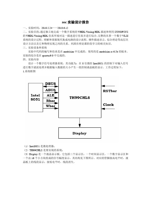
四、实验内容设计一个数字信号处理器系统,其功能为:在8位微控Intel8051的控制下对输入信号进行数字滤波处理并根据输入数据的大小产生一组控制液晶板的显示。
工作过程如下:1.系统框图(1)Intel8051是微处理器;(2)TH99CHLS是要实现的系统;(3)Display是一个液晶显示板。
它包括三个显示区:一个时间显示区,一个数字显示区和一个由16个小方块组成的信号幅度显示,其结构见下图所示。
对应的管脚接高电平时,液晶板上的线段显示;接低电平时,线段消失。
2.工作过程(1)在外部信号PEbar的控制下,芯片从端口in读入一个八位数据;(2)在(1)中输入的数据与微处理器给出的另一个八位数据进行按位“与”操作;(3)在(2)中处理过的数据经数字滤波后从端口out输出;(4)TH98CHLS内部产生一组时间信号,包括时和分,其格式为:(hh:mm)。
这组时间信号的初始值由微处理器给出,微处理器可以随时对时间信号进行修改;(5)送往液晶显示板的信号有三组:a. (4)中产生的时间信号,经七段译码后从端口hour和minute出;b. (3)中经数字滤波的信号,在转换成十进制并做七段译码后,百位经端口d00,十位经端口d10,个位经端口d01送出;c. (3)中经数字滤波的信号,在经过xy 压缩后通过端口ap送出;五、数据通道由滤波器公式可知采用通常的调配方法,用四个步长来实现。
SoC处理器的电源管理系统设计
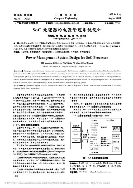
—262—SoC 处理器的电源管理系统设计何允灵,秦 娟,王 佳,倪 明,柴小丽(华东计算技术研究所,上海 200233)摘 要:从软硬件角度探讨SoC 处理器电源管理系统的设计,分析SoC 处理器PMU 的特征,根据其应用需求讨论有关PMIC 的设计问题,包括:电源IC 内部结构及选型原则,数字PMIC 与传统电源IC 相比所做的改进,一种新的电源管理总线——PMBus 和一种高度整合的PMIC 应用。
从嵌入式操作系统的角度分析了动态电源管理系统的设计。
关键词:片上系统;电源管理单元;电源管理芯片;低压差线性稳压器;开关电源;数字电源管理Power Management System Design for SoC ProcessorHE Yun-ling, QIN Juan, WANG Jia, NI Ming, CHAI Xiao-li(East-China Institute of Computer Technology, Shanghai 200233)【Abstract 】This paper studies the power management system design for the System-on-Chip(SoC) processor technology. The characteristic of the processor’s Power Management Unit(PMU) is analyzed. According to its application demands, it discusses the design problems of Power Management IC(PMIC), which includes: the interior architecture of the power IC and its selection principle, the improvement of the digital PMIC in contrast with the traditional power IC, the application of a new power management bus called PMBus and a highly integrated PMIC. It analyzes the design of Dynamic Power Management(DPM), which is a module in the embedded operating system.【Key words 】System-on-Chip(SoC); Power Management Unit(PMU); Power Management IC(PMIC); Low Dropout Regulator(LDO); switching regulator; digital power management计 算 机 工 程Computer Engineering 第34卷 第16期Vol.34 No.16 2008年8月August 2008·工程应用技术与实现·文章编号:1000—3428(2008)16—0262—03文献标识码:A中图分类号:TP303随着微电子技术和半导体工艺的迅速发展,一个复杂的系统能被集成在一个硅片上,片上系统(System-on-Chip, SoC)的时代已经来临。
高速SPI主模式控制器的制作流程
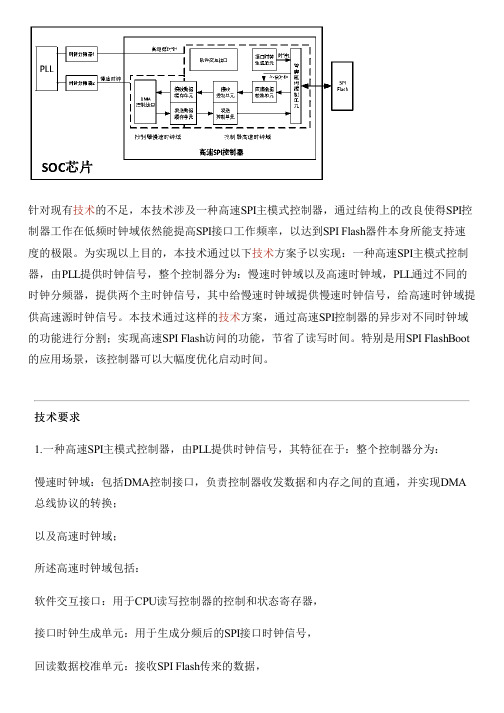
针对现有技术的不足,本技术涉及一种高速SPI主模式控制器,通过结构上的改良使得SPI控制器工作在低频时钟域依然能提高SPI接口工作频率,以达到SPI Flash器件本身所能支持速度的极限。
为实现以上目的,本技术通过以下技术方案予以实现:一种高速SPI主模式控制器,由PLL提供时钟信号,整个控制器分为:慢速时钟域以及高速时钟域,PLL通过不同的时钟分频器,提供两个主时钟信号,其中给慢速时钟域提供慢速时钟信号,给高速时钟域提供高速源时钟信号。
本技术通过这样的技术方案,通过高速SPI控制器的异步对不同时钟域的功能进行分割;实现高速SPI Flash访问的功能,节省了读写时间。
特别是用SPI FlashBoot 的应用场景,该控制器可以大幅度优化启动时间。
技术要求1.一种高速SPI主模式控制器,由PLL提供时钟信号,其特征在于:整个控制器分为:慢速时钟域:包括DMA控制接口,负责控制器收发数据和内存之间的直通,并实现DMA 总线协议的转换;以及高速时钟域;所述高速时钟域包括:软件交互接口:用于CPU读写控制器的控制和状态寄存器,接口时钟生成单元:用于生成分频后的SPI接口时钟信号,回读数据校准单元:接收SPI Flash传来的数据,接收控制单元和发送控制单元:处理收发SPI Flash数据信号,以及管脚延时控制单元:用于实现SPI的高速IO的时序控制;PLL通过不同的时钟分频器,提供两个主时钟信号,其中给慢速时钟域提供慢速时钟信号,给高速时钟域提供高速源时钟信号。
2.如权利要求1所述的一种高速SPI主模式控制器,其特征在于:接口时钟生成单元给管脚延时控制单元提供时钟信号,管脚延时控制单元连接回读数据校准单元并给回读数据校准单元提供补偿时钟,回读数据校准单元连接接收控制单元。
3.如权利要求1或2所述的一种高速SPI主模式控制器,其特征在于:高速源时钟信号的频率固定为SPI接口时钟信号频率的整数倍。
4.如权利要求3所述的一种高速SPI主模式控制器,其特征在于:高速源时钟信号的频率固定为SPI接口时钟信号频率的2倍,此时接口时钟生成单元生成二分频后的SPI接口时钟。
EFR32BG22无线Gecko SoC产品系列数据表说明书
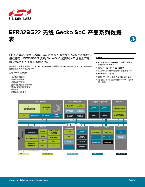
EFR32BG22 无线 Gecko SoC 产品系列数据表EFR32BG22无线 Gecko SoC 产品系列是无线 Gecko 产品组合的组成部分。
EFR32BG22无线 GeckoSoC 是实现 IoT 设备上节能Bluetooth 5.2 连网的理想之选。
这款单芯片解决方案结合了 76.8 MHz Cortex-M33 和高性能 2.4 GHz 无线电,旨在为 IoT 连接应用提供行业领先的节能无线 SoC 。
无线 Gecko 应用包括:主要特点•32 位 ARM® Cortex®-M33 内核,最高工作频率为 76.8 MHz•最高 512 kB 闪存和 32 kB RAM •低有功电流和睡眠电流的节能型射频内核•Bluetooth 5.2 测向•集成 PA ,TX 功率高达 6 dBm (2.4 GHz)•通过信任根和安全加载程序 (RTSL) 进行的安全启动•资产标签和信标•消费电子遥控器•便携式医疗器械•蓝牙网状网络低功耗节点•体育、健身和健康设备•联网家庭•建筑自动化及安全Lowest power mode with peripheral operational:EM4—ShutoffEM3—StopEM2—Deep SleepEM1—SleepEM0—Active| Building a more connected world.Rev. 1.11.功能列表EFR32BG22 突出功能如下所列。
•低功耗无线片上系统•高性能 32 位 76.8 MHz MHz ARM Cortex®-M33,带有 DSP 指令和浮点单元,可实现高效的信号处理•高达 512 kB 的闪存程序存储器•高达 32 kB 的 RAM 数据存储器•2.4 GHz 无线电操作•射频性能•在 125 kbps GFSK 的条件下,灵敏度为-106.7 dBm•在 1 Mbit/s GFSK 的条件下,灵敏度为-98.9 dBm•在 2 Mbit/s GFSK 的条件下,灵敏度为-96.2 dBm•TX 功率高达 6 dBm•无线电接收电流为2.5 mA•在 0 dBm 输出功率的条件下,无线电传输电流为3.4 mA•在 6 dBm 输出功率的条件下,无线电传输电流为7.5 mA•低系统能耗•RX 电流为3.6 mA (1 Mbps GFSK)•在 0 dBm 输出功率的条件下,TX 电流为4.1 mA•在 6 dBm 输出功率的条件下,TX 电流为8.2 mA•在 76.8 MHz 活动模式 (EM0) 下,运行功耗为27 μA/MHz•1.40 μA EM2 深度睡眠电流(保留 32 kB RAM,RTC 从 LFXO 中运行)•1.75 μA EM2 深度睡眠电流(保留 32 kB RAM,RTC 从 PrecisionLFRCO 中运行)•0.17 μA EM4 电流•支持的调制格式•2 (G)FSK,可配置完整波形•OQPSK DSSS•(G)MSK•协议支持•Bluetooth 低功耗 (Bluetooth 5.2)•采用到达角 (AoA) 和发射角 (AoD) 实现测向•专有•广泛的 MCU 外围设备选择•模拟数字转换器 (ADC)•12 位,1 Msps•16 位,76.9 ksps•高达 26 个带有输出状态保持和异步中断功能的通用 I/O 引脚•8 信道 DMA 控制器•12 信道外围设备反射系统 (PRS)•4 个 16 位定时器/计数器(3 个比较/捕获/PWM 通道)•1 个 32 位定时器/计数器(3 个比较/捕获/PWM 通道)•32 位实时计数器•24 位低能耗定时器,用于波形生成•1 个看门狗定时器•2 个通用同步/异步接收器/传输器 (UART/SPI/SmartCard (ISO 7816)/ IrDA/I2S)•1 个增强型通用异步接收器/传输器 (EUART)•2 个 I2C 接口,带 SMBus 支持•数字麦克风接口 (PDM)•32 KHz 睡眠晶体更换为精密低频 RC 振荡器•可选 OOK 模式的 RFSENSE•单点校准后具有 +/-1.5 摄氏度精度的芯片温度传感器•宽工作范围•单电源1.71 至 3.8 V•-40°C 至 125°C•安全特性•通过信任根和安全加载程序 (RTSL) 进行的安全启动•硬件加密加速,适用于 AES128/256、SHA-1、SHA-2(高达 256位)、ECC(高达 256 位)、ECDSA 和 ECDH•符合 NIST SP800-90 和 AIS-31 标准的真随机数生成器 (TRNG)•ARM® TrustZone®•使用锁定/解锁功能进行安全调试•封装•QFN40 5 毫米 × 5 毫米 × 0.85 毫米•QFN32 4 毫米 × 4 毫米 × 0.85 毫米•TQFN32 4 毫米 × 4 毫米 × 0.30 毫米EFR32BG22 无线 Gecko SoC 产品系列数据表功能列表1EFR32BG22 Wireless Gecko SoC Family Data SheetOrdering Information 2. Ordering InformationTable 2.1. Ordering InformationLE Long Range (125 kbps and 500 kbps) PHYs are only supported on part numbers which include AoA/AoD direction-finding capability. | Building a more connected world.Rev. 1.1 | 3Table of Contents1. Feature List (2)2. Ordering Information (3)3. System Overview (7)3.1 Introduction (7)3.2 Radio (7)3.2.1 Antenna Interface (7)3.2.2 Fractional-N Frequency Synthesizer (8)3.2.3 Receiver Architecture (8)3.2.4 Transmitter Architecture (8)3.2.5 Packet and State Trace (8)3.2.6 Data Buffering (8)3.2.7 Radio Controller (RAC) (8)3.2.8 RFSENSE Interface (9)3.3 General Purpose Input/Output (GPIO) (9)3.4 Clocking (9)3.4.1 Clock Management Unit (CMU) (9)3.4.2 Internal and External Oscillators (9)3.5 Counters/Timers and PWM (9)3.5.1 Timer/Counter (TIMER) (9)3.5.2 Low Energy Timer (LETIMER) (10)3.5.3 Real Time Clock with Capture (RTCC) (10)3.5.4 Back-Up Real Time Counter (BURTC) (10)3.5.5 Watchdog Timer (WDOG) (10)3.6 Communications and Other Digital Peripherals (10)3.6.1 Universal Synchronous/Asynchronous Receiver/Transmitter (USART) (10)3.6.2 Enhanced Universal Asynchronous Receiver/Transmitter (EUART) (10)3.6.3 Inter-Integrated Circuit Interface (I2C) (10)3.6.4 Peripheral Reflex System (PRS) (11)3.6.5 Pulse Density Modulation (PDM) Interface (11)3.7 Security Features (11)3.7.1 Secure Boot with Root of Trust and Secure Loader (RTSL) (11)3.7.2 Cryptographic Accelerator (11)3.7.3 True Random Number Generator (11)3.7.4 Secure Debug with Lock/Unlock (12)3.8 Analog (12)3.8.1 Analog to Digital Converter (IADC) (12)3.9 Power (13)3.9.1 Energy Management Unit (EMU) (13)3.9.2 Voltage Scaling (13)3.9.3 DC-DC Converter (13)3.9.4 Power Domains (13)3.10 Reset Management Unit (RMU) (14)3.11 Core and Memory (14)3.11.1 Processor Core (14)3.11.2 Memory System Controller (MSC) (14)3.11.3 Linked Direct Memory Access Controller (LDMA) (14)3.12 Memory Map (15)3.13 Configuration Summary (16)4. Electrical Specifications (17)4.1 Electrical Characteristics (17)4.2 Absolute Maximum Ratings (18)4.3 General Operating Conditions (19)4.4 DC-DC Converter (21)4.4.1 DC-DC Operating Limits (23)4.5 Thermal Characteristics (24)4.6 Current Consumption (25)4.6.1 MCU current consumption using DC-DC at 3.0 V input (25)4.6.2 MCU current consumption at 3.0 V (27)4.6.3 MCU current consumption at 1.8 V (29)4.6.4 Radio current consumption at 3.0V using DCDC (31)4.7 Flash Characteristics (33)4.8 Wake Up, Entry, and Exit times (34)4.9 RFSENSE Low-energy Wake-on-RF (35)4.10 2.4 GHz RF Transceiver Characteristics (36)4.10.1 RF Transmitter Characteristics (36)4.10.2 RF Receiver Characteristics (43)4.11 Oscillators (49)4.11.1 High Frequency Crystal Oscillator (49)4.11.2 Low Frequency Crystal Oscillator (50)4.11.3 High Frequency RC Oscillator (HFRCO) (51)4.11.4 Fast Start_Up RC Oscillator (FSRCO) (52)4.11.5 Precision Low Frequency RC Oscillator (LFRCO) (53)4.11.6 Ultra Low Frequency RC Oscillator (53)4.12 GPIO Pins (3V GPIO pins) (54)4.13 Analog to Digital Converter (IADC) (56)4.14 Temperature Sense (58)4.15 Brown Out Detectors (59)4.15.1 DVDD BOD (59)4.15.2 LE DVDD BOD (59)4.15.3 AVDD and IOVDD BODs (60)4.16 PDM Timing Specifications (61)4.16.1 Pulse Density Modulator (PDM), Common DBUS (61)4.17 USART SPI Main Timing (62)4.17.1 SPI Main Timing, Voltage Scaling = VSCALE2 (63)4.17.2 SPI Main Timing, Voltage Scaling = VSCALE1 (63)4.18 USART SPI Secondary Timing (64)4.18.1 SPI Secondary Timing, Voltage Scaling = VSCALE2 (64)4.18.2 SPI Secondary Timing, Voltage Scaling = VSCALE1 (65)4.19 I2C Electrical Specifications (66)4.19.1 I2C Standard-mode (Sm) (66)4.19.2 I2C Fast-mode (Fm) (67)4.19.3 I2C Fast-mode Plus (Fm+) (68)4.20 Typical Performance Curves (68)4.20.1 Supply Current (69)4.20.2 RF Characteristics (71)4.20.3 DC-DC Converter (72)4.20.4 IADC (72)5. Typical Connections (73)5.1 Power (73)5.2 RF Matching Networks (74)5.2.1 2.4 GHz Matching Network (74)5.3 Other Connections (75)6. Pin Definitions (76)6.1 QFN32 Device Pinout (76)6.2 QFN40 Device Pinout (78)6.3 TQFN32 Device Pinout (80)6.4 Alternate Function Table (81)6.5 Analog Peripheral Connectivity (82)6.6 Digital Peripheral Connectivity (83)7. QFN32 Package Specifications (86)7.1 QFN32 Package Dimensions (86)7.2 QFN32 PCB Land Pattern (88)7.3 QFN32 Package Marking (90)8. TQFN32 Package Specifications (91)8.1 TQFN32 Package Dimensions (91)8.2 TQFN32 PCB Land Pattern (93)8.3 TQFN32 Package Marking (95)9. QFN40 Package Specifications (96)9.1 QFN40 Package Dimensions (96)9.2 QFN40 PCB Land Pattern (98)9.3 QFN40 Package Marking (99)10. Revision History (100)3. System Overview3.1 IntroductionThe EFR32 product family combines an energy-friendly MCU with a high performance radio transceiver. The devices are well suited for secure connected IoT multi-protocol devices requiring high performance and low energy consumption. This section gives a short intro-duction to the full radio and MCU system. The detailed functional description can be found in the EFR32xG22 Reference Manual.A block diagram of the EFR32BG22 family is shown in Figure 3.1 Detailed EFR32BG22 Block Diagram on page 7. The diagram shows a superset of features available on the family, which vary by OPN. For more information about specific device features, consult Ordering Information .RESETnPDnPCnPBnPAnRF2G4_IODVDDVREGVDD VREGSW AVDD PAVDD RFVDD DECOUPLEIOVDD Figure 3.1. Detailed EFR32BG22 Block Diagram3.2 RadioThe EFR32BG22 Wireless Gecko features a highly configurable radio transceiver supporting the Bluetooth Low Energy wireless proto-col.3.2.1 Antenna InterfaceThe 2.4 GHz antenna interface consists of a single-ended pin (RF2G4_IO). The external components for the antenna interface in typi-cal applications are shown in the RF Matching Networks section.Rev. 1.1 | 73.2.2 Fractional-N Frequency SynthesizerThe EFR32BG22 contains a high performance, low phase noise, fully integrated fractional-N frequency synthesizer. The synthesizer is used in receive mode to generate the LO frequency for the down-conversion mixer. It is also used in transmit mode to directly generate the modulated RF carrier.The fractional-N architecture provides excellent phase noise performance, frequency resolution better than 100 Hz, and low energy consumption. The synthesizer’s fast frequency settling allows for very short receiver and transmitter wake up times to reduce system energy consumption.3.2.3 Receiver ArchitectureThe EFR32BG22 uses a low-IF receiver architecture, consisting of a Low-Noise Amplifier (LNA) followed by an I/Q down-conversion mixer. The I/Q signals are further filtered and amplified before being sampled by the IF analog-to-digital converter (IFADC).The IF frequency is configurable from 150 kHz to 1371 kHz. The IF can further be configured for high-side or low-side injection, provid-ing flexibility with respect to known interferers at the image frequency.The Automatic Gain Control (AGC) module adjusts the receiver gain to optimize performance and avoid saturation for excellent selec-tivity and blocking performance. The 2.4 GHz radio is calibrated at production to improve image rejection performance.Demodulation is performed in the digital domain. The demodulator performs configurable decimation and channel filtering to allow re-ceive bandwidths ranging from 0.1 to 2530 kHz. High carrier frequency and baud rate offsets are tolerated by active estimation and compensation. Advanced features supporting high quality communication under adverse conditions include forward error correction by block and convolutional coding as well as Direct Sequence Spread Spectrum (DSSS).A Received Signal Strength Indicator (RSSI) is available for signal quality metrics, for level-based proximity detection, and for RF chan-nel access by Collision Avoidance (CA) or Listen Before Talk (LBT) algorithms. An RSSI capture value is associated with each received frame and the dynamic RSSI measurement can be monitored throughout reception.3.2.4 Transmitter ArchitectureThe EFR32BG22 uses a direct-conversion transmitter architecture. For constant envelope modulation formats, the modulator controls phase and frequency modulation in the frequency synthesizer. Transmit symbols or chips are optionally shaped by a digital shaping filter. The shaping filter is fully configurable, including the BT product, and can be used to implement Gaussian or Raised Cosine shap-ing.Carrier Sense Multiple Access - Collision Avoidance (CSMA-CA) or Listen Before Talk (LBT) algorithms can be automatically timed by the EFR32BG22. These algorithms are typically defined by regulatory standards to improve inter-operability in a given bandwidth be-tween devices that otherwise lack synchronized RF channel access.3.2.5 Packet and State TraceThe EFR32BG22 Frame Controller has a packet and state trace unit that provides valuable information during the development phase. It features:•Non-intrusive trace of transmit data, receive data and state information•Data observability on a single-pin UART data output, or on a two-pin SPI data output•Configurable data output bitrate / baudrate•Multiplexed transmitted data, received data and state / meta information in a single serial data stream3.2.6 Data BufferingThe EFR32BG22 features an advanced Radio Buffer Controller (BUFC) capable of handling up to 4 buffers of adjustable size from 64 bytes to 4096 bytes. Each buffer can be used for RX, TX or both. The buffer data is located in RAM, enabling zero-copy operations.3.2.7 Radio Controller (RAC)The Radio Controller controls the top level state of the radio subsystem in the EFR32BG22. It performs the following tasks:•Precisely-timed control of enabling and disabling of the receiver and transmitter circuitry•Run-time calibration of receiver, transmitter and frequency synthesizer•Detailed frame transmission timing, including optional LBT or CSMA-CA3.2.8 RFSENSE InterfaceThe RFSENSE block allows the device to remain in EM2, EM3 or EM4 and wake when RF energy above a specified threshold is detec-ted. When operated in selective mode, the RFSENSE block performs OOK preamble and sync word detection, preventing false wake-up events.3.3 General Purpose Input/Output (GPIO)EFR32BG22 has up to 26 General Purpose Input/Output pins. Each GPIO pin can be individually configured as either an output or input. More advanced configurations including open-drain, open-source, and glitch-filtering can be configured for each individual GPIO pin. The GPIO pins can be overridden by peripheral connections, like SPI communication. Each peripheral connection can be routed to several GPIO pins on the device. The input value of a GPIO pin can be routed through the Peripheral Reflex System to other peripher-als. The GPIO subsystem supports asynchronous external pin interrupts.All of the pins on ports A and port B are EM2 capable. These pins may be used by Low-Energy peripherals in EM2/3 and may also be used as EM2/3 pin wake-ups. Pins on ports C and D are latched/retained in their current state when entering EM2 until EM2 exit upon which internal peripherals could once again drive those pads.A few GPIOs also have EM4 wake functionality. These pins are listed in the Alternate Function Table.3.4 Clocking3.4.1 Clock Management Unit (CMU)The Clock Management Unit controls oscillators and clocks in the EFR32BG22. Individual enabling and disabling of clocks to all periph-eral modules is performed by the CMU. The CMU also controls enabling and configuration of the oscillators. A high degree of flexibility allows software to optimize energy consumption in any specific application by minimizing power dissipation in unused peripherals and oscillators.3.4.2 Internal and External OscillatorsThe EFR32BG22 supports two crystal oscillators and fully integrates four RC oscillators, listed below.• A high frequency crystal oscillator (HFXO) with integrated load capacitors, tunable in small steps, provides a precise timing refer-ence for the MCU. The HFXO provides excellent RF clocking performance using a 38.4 MHz crystal. The HFXO can also support an external clock source such as a TCXO for applications that require an extremely accurate clock frequency over temperature.• A 32.768 kHz crystal oscillator (LFXO) provides an accurate timing reference for low energy modes.•An integrated high frequency RC oscillator (HFRCO) is available for the MCU system, when crystal accuracy is not required. The HFRCO employs fast start-up at minimal energy consumption combined with a wide frequency range, from 1 MHz to 76.8 MHz.•An integrated fast start-up RC oscillator (FSRCO) that runs at a fixed 20 MHz•An integrated low frequency 32.768 kHz RC oscillator (LFRCO) for low power operation without an external crystal. Precision mode enables periodic recalibration against the 38.4 MHz HFXO crystal to improve accuracy to +/- 500 ppm, suitable for BLE sleep inter-val timing.•An integrated ultra-low frequency 1 kHz RC oscillator (ULFRCO) is available to provide a timing reference at the lowest energy con-sumption in low energy modes.3.5 Counters/Timers and PWM3.5.1 Timer/Counter (TIMER)TIMER peripherals keep track of timing, count events, generate PWM outputs and trigger timed actions in other peripherals through the Peripheral Reflex System (PRS). The core of each TIMER is a 16-bit or 32-bit counter with up to 3 compare/capture channels. Each channel is configurable in one of three modes. In capture mode, the counter state is stored in a buffer at a selected input event. In compare mode, the channel output reflects the comparison of the counter to a programmed threshold value. In PWM mode, the TIMER supports generation of pulse-width modulation (PWM) outputs of arbitrary waveforms defined by the sequence of values written to the compare registers. In addition some timers offer dead-time insertion.See 3.13 Configuration Summary for information on the feature set of each timer.3.5.2 Low Energy Timer (LETIMER)The unique LETIMER is a 24-bit timer that is available in energy mode EM0 Active, EM1 Sleep, EM2 Deep Sleep, and EM3 Stop. This allows it to be used for timing and output generation when most of the device is powered down, allowing simple tasks to be performed while the power consumption of the system is kept at an absolute minimum. The LETIMER can be used to output a variety of wave-forms with minimal software intervention. The LETIMER is connected to the Peripheral Reflex System (PRS), and can be configured to start counting on compare matches from other peripherals such as the Real Time Clock.3.5.3 Real Time Clock with Capture (RTCC)The Real Time Clock with Capture (RTCC) is a 32-bit counter providing timekeeping down to EM3. The RTCC can be clocked by any of the on-board low-frequency oscillators, and it is capable of providing system wake-up at user defined intervals.A secondary RTC is used by the RF protocol stack for event scheduling, leaving the primary RTCC block available exclusively for appli-cation software.3.5.4 Back-Up Real Time Counter (BURTC)The Back-Up Real Time Counter (BURTC) is a 32-bit counter providing timekeeping in all energy modes, including EM4. The BURTC can be clocked by any of the on-board low-frequency oscillators, and it is capable of providing system wake-up at user-defined inter-vals.3.5.5 Watchdog Timer (WDOG)The watchdog timer can act both as an independent watchdog or as a watchdog synchronous with the CPU clock. It has windowed monitoring capabilities, and can generate a reset or different interrupts depending on the failure mode of the system. The watchdog can also monitor autonomous systems driven by the Peripheral Reflex System (PRS).3.6 Communications and Other Digital Peripherals3.6.1 Universal Synchronous/Asynchronous Receiver/Transmitter (USART)The Universal Synchronous/Asynchronous Receiver/Transmitter is a flexible serial I/O module. It supports full duplex asynchronous UART communication with hardware flow control as well as RS-485, SPI, MicroWire and 3-wire. It can also interface with devices sup-porting:•ISO7816 SmartCards•IrDA•I2S3.6.2 Enhanced Universal Asynchronous Receiver/Transmitter (EUART)The Enhanced Universal Asynchronous Receiver/Transmitter supports full duplex asynchronous UART communication with hardware flow control, RS-485 and IrDA support. In EM0 and EM1 the EUART provides a high-speed, buffered communication interface.When routed to GPIO ports A or B, the EUART may also be used in a low-energy mode and operate in EM2. A 32.768 kHz clock source allows full duplex UART communication up to 9600 baud.3.6.3 Inter-Integrated Circuit Interface (I2C)The I2C module provides an interface between the MCU and a serial I2C bus. It is capable of acting as a main or secondary interface and supports multi-drop buses. Standard-mode, fast-mode and fast-mode plus speeds are supported, allowing transmission rates from 10 kbit/s up to 1 Mbit/s. Bus arbitration and timeouts are also available, allowing implementation of an SMBus-compliant system. The interface provided to software by the I2C module allows precise timing control of the transmission process and highly automated trans-fers. Automatic recognition of addresses is provided in active and low energy modes. Note that not all instances of I2C are available in all energy modes.3.6.4 Peripheral Reflex System (PRS)The Peripheral Reflex System provides a communication network between different peripheral modules without software involvement. Peripheral modules producing Reflex signals are called producers. The PRS routes Reflex signals from producers to consumer periph-erals which in turn perform actions in response. Edge triggers and other functionality such as simple logic operations (AND, OR, NOT) can be applied by the PRS to the signals. The PRS allows peripherals to act autonomously without waking the MCU core, saving power.3.6.5 Pulse Density Modulation (PDM) InterfaceThe PDM module provides a serial interface and decimation filter for Pulse Density Modulation (PDM) microphones, isolated Sigma-delta ADCs, digital sensors and other PDM or sigma delta bit stream peripherals. A programmable Cascaded Integrator Comb (CIC) filter is used to decimate the incoming bit streams. PDM supports stereo or mono input data and DMA transfer.3.7 Security FeaturesThe following security features are available on the EFR32BG22:•Secure Boot with Root of Trust and Secure Loader (RTSL)•Cryptographic Accelerator•True Random Number Generator (TRNG)•Secure Debug with Lock/Unlock3.7.1 Secure Boot with Root of Trust and Secure Loader (RTSL)The Secure Boot with RTSL authenticates a chain of trusted firmware that begins from an immutable memory (ROM).It prevents malware injection, prevents rollback, ensures that only authentic firmware is executed and protects Over The Air updates. More information on this feature can be found in the Application Note AN1218: Series 2 Secure Boot with RTSL.3.7.2 Cryptographic AcceleratorThe Cryptographic Accelerator is an autonomous hardware accelerator which supports AES encryption and decryption with 128/192/256-bit keys, Elliptic Curve Cryptography (ECC) to support public key operations and hashes.Supported block cipher modes of operation for AES include:•ECB (Electronic Code Book)•CTR (Counter Mode)•CBC (Cipher Block Chaining)•CFB (Cipher Feedback)•GCM (Galois Counter Mode)•CBC-MAC (Cipher Block Chaining Message Authentication Code)•GMAC (Galois Message Authentication Code)•CCM (Counter with CBC-MAC)The Cryptographic Accelerator accelerates Elliptical Curve Cryptography and supports the NIST (National Institute of Standards and Technology) recommended curves including P-192 and P-256 for ECDH(Elliptic Curve Diffie-Hellman) key derivation and ECDSA (El-liptic Curve Digital Signature Algorithm) sign and verify operations.Supported hashes include SHA-1, SHA2/224, and SHA-2/256.This implementation provides a fast and energy efficient solution to state of the art cryptographic needs.3.7.3 True Random Number GeneratorThe True Random Number Generator module is a non-deterministic random number generator that harvests entropy from a thermal energy source. It includes start-up health tests for the entropy source as required by NIST SP800-90B and AIS-31 as well as online health tests required for NIST SP800-90C.The TRNG is suitable for periodically generating entropy to seed an approved pseudo random number generator.3.7.4 Secure Debug with Lock/UnlockFor obvious security reasons, it is critical for a product to have its debug interface locked before being released in the field.In addition, the EFR32BG22 also provides a secure debug unlock function that allows authenticated access based on public key cryp-tography. This functionality is particularly useful for supporting failure analysis while maintaining confidentiality of IP and sensitive end-user data.More information on this feature can be found in the Application Note AN1190: EFR32xG2x Secure Debug.3.8 Analog3.8.1 Analog to Digital Converter (IADC)The IADC is a hybrid architecture combining techniques from both SAR and Delta-Sigma style converters. It has a resolution of 12 bits at 1 Msps and 16 bits at up to 76.9 ksps. Hardware oversampling reduces system-level noise over multiple front-end samples. The IADC includes integrated voltage reference options. Inputs are selectable from a wide range of sources, including pins configurable as either single-ended or differential.3.9 PowerThe EFR32BG22 has an Energy Management Unit (EMU) and efficient integrated regulators to generate internal supply voltages. Only a single external supply voltage is required, from which all internal voltages are created. An optional integrated DC-DC buck regulator can be utilized to further reduce the current consumption. The DC-DC regulator requires one external inductor and one external capaci-tor.The EFR32BG22 device family includes support for internal supply voltage scaling, as well as two different power domains groups for peripherals. These enhancements allow for further supply current reductions and lower overall power consumption.3.9.1 Energy Management Unit (EMU)The Energy Management Unit manages transitions of energy modes in the device. Each energy mode defines which peripherals and features are available and the amount of current the device consumes. The EMU can also be used to implement system-wide voltage scaling and turn off the power to unused RAM blocks to optimize the energy consumption in the target application. The DC-DC regula-tor operation is tightly integrated with the EMU.3.9.2 Voltage ScalingThe EFR32BG22 supports supply voltage scaling for the LDO powering DECOUPLE, with independent selections for EM0 / EM1 and EM2 / EM3. Voltage scaling helps to optimize the energy efficiency of the system by operating at lower voltages when possible. The EM0 / EM1 voltage scaling level defaults to VSCALE2, which allows the core to operate in active mode at full speed. The intermediate level, VSCALE1, allows operation in EM0 and EM1 at up to 40 MHz. The lowest level, VSCALE0, can be used to conserve power fur-ther in EM2 and EM3. The EMU will automatically switch the target voltage scaling level when transitioning between energy modes.3.9.3 DC-DC ConverterThe DC-DC buck converter covers a wide range of load currents, provides high efficiency in energy modes EM0, EM1, EM2 and EM3, and can supply up to 60 mA for device and radio operation. RF noise mitigation allows operation of the DC-DC converter without signifi-cantly degrading sensitivity of radio components. An on-chip supply-monitor signals when the supply voltage is low to allow bypass of the regulator via programmable software interrupt. It employs soft switching at boot and DCDC regulating-to-bypass transitions to limit the max supply slew-rate and mitigate inrush current.3.9.4 Power DomainsThe EFR32BG22 has three peripheral power domains for operation in EM2 and EM3, as well as the ability to selectively retain configu-rations for EM0/EM1 peripherals. A small set of peripherals always remain powered on in EM2 and EM3, including all peripherals which are available in EM4. If all of the peripherals in PD0B or PD0C are configured as unused, that power domain will be powered off in EM2 or EM3, reducing the overall current consumption of the device. Likewise, if the application can tolerate the setup time to re-configure used EM0/EM1 peripherals on wake, register retention for these peripherals can be disabled to further reduce the EM2 or EM3 current.Table 3.1. Peripheral Power Subdomains。
精选6SoC的功耗
锁相环是一种基于闭环控制系统的窄带跟踪系统,广泛应用于频率合成、调制解调、同步提取、测距测量等。在嵌入式微处理器中,需要使用PLL合成指定频率的时钟信号。
S3C44B0X的锁相环电路方框图
S3C44B0X的PLL输出的时钟受控于PLLCON设置
S3C44B0X锁相环输出时钟的频率
液晶屏慢空闲模式(SL_IDLE模式)
LCD控制器工作。CPU内核和其他外设的时钟都停止。SL_IDLE模式比空闲模式功耗低。进入SL_IDLE模式之前:必须进入低速模式PLL必须关闭。进入低速模式关闭PLL之后,要向CLKCON寄存器写入0x46(LCDC使能,IDLE使能, SL_IDLE使能),然后进入SL_IDLE模式。
CLKCON位定义(上)
S3C44B0X的时钟控制寄存器
CLKCON位定义(下)
S3C44B0X的空闲模式
停止对CPU内核的时钟供给总线控制器、存储控制器、中断控制器和电源管理模块继续正常运行。保留所有对外部设备的时钟信号供给。在空闲模式下,总功耗不包含CPU内核的功耗。任何中断请求都能够把CPU从空闲模式中唤醒。
动态功耗
在状态转移过程中为电容充电所消耗的能量。将容量为C的电容充电到VDD 所需要的能量为 CVDD2如果电路运行的频率为f,并且所有的电容都从1变化到0(或者相反),则每秒钟电容充电的次数为f/2次。因此,总的动态功耗为:Pdynamic = ½CVDD2f
静态功耗
在没有门转换时的功耗。由漏电流IDD引起静态功耗为:Pstatic = IDDVDD
感谢您的下载观看
SDIV
[1:0]
后分频控制值,S分频系数
0x0
S3C44B0X锁相环输出时钟设置举例
重庆大学SoC设计第2章
• 模块设计及IP复用(Module Design & IP
Reuse)
硬件设计定义说明描述芯片总体结构、规格参数、模块 划分、使用的总线,以及各个模块的详细定义等。
对于需要重新设计的模块进行设计;对于可复用的IP核 ,通常由于总线接口标准不一致需要做一定的修改。
基于标准单元的SoC芯片设计流程
Motion Estimation Accelerator IP External Memory External Memory Controller
ARM920T
DSP CHIP
AHB
On chip memory controller and memory
Direct Memory Access (DMA)
基于标准单元的SoC芯片设计流程
• 形式验证(Formal Verification)
• 可测性电路插入(DFT,Design for Test)
形式验证也是一种静态验证方法。 在整个设计流程中会多次引入形式验证用于比较RTL代 码之间、门级网表与RTL代码之间,以及门级网表之间 在修改之前与修改之后功能的一致性。 可测性设计是SoC设计中的重要一步。通常,对于逻辑 电路采用扫描链的可测试结构,对于芯片的输入/输出端 口采用边界扫描的可测试结构。基本思想是通过插入扫 描链,增加电路内部节点的可控性和可观测性,以达到 提高测试效率的目的。一般在逻辑综合或物理综合后进 行扫描电路的插入和优化。
Slide 18
硬件顶层设计-例子
确定软硬件划分
• • •
软件 灵活性好 性能有待提高 充分利用硬件资源,如处理器 硬件 不够灵活 达到较好的功耗/性能折中 软硬件划分 把系统功能划分为软件部分和硬件部分 定义和明确软硬件接口和通信协议 需要经验丰富的人员依靠人工完成 一个包含可重用核和可重用软件的库,有助于软硬件评估和划分
第1章 SOPC技术应用概述
1
SOPC 技术应用
第1章 SOPC概述
1.1 1.2 1.3 1.4 1.5 基本概念 SOPC设计流程 支持SOPC的可编程逻辑器件 支持SOPC技术的EDA工具 支持SOPC的硬件描述语言
2018/4/8
2
1.1 基本概念
1、SOC(System On a Chip) SOC称为片上系统,它是指将一个完整产品的功能 集成在一个芯片上或芯片组上。 SOC芯片中可以包含微处理器CPU、数字信号处理 器DSP、存储器(ROM、RAM、Flash等)、总线和 总线控制器、外围设备接口等,还可以包含数模混合 电路(放大器、比较器、A/D和D/A转换器、锁相环 等),甚至包含传感器、微机电和微光电单元等外围 部件。
2018/4/8
3
2、 SOPC (System On a Programmable Chip) SOPC称为可编程片上系统,它是基于可编程 逻辑器件PLD(FPGA)可重构的SOC。 SOPC集成了硬核或软核CPU、DSP、锁相环 (PLL)、存储器、I/O接口及可编程逻辑,可以 灵活高效地解决SOC方案,而且设计周期短,设 计成本低,一般只需要一台配有SOPC开发软件的 PC机和一台SOPC试验开发系统(或开发板), 就可以进行SOPC的设计与开发。目前,SOPC技 术已成为倍受众多中小企业、研究所和大专院校 青睐的设计技术。
FPGA
键盘 嵌入式 CPU核 PIO Timer PLL 存储器
RAM
IP模块
LED
通信口
UART
ROM
DSP
LCD
2018/4/8
8
(1)嵌入式微处理器 嵌入式微处理器是嵌入式系统的核心,有硬 核和软核之分。常用的嵌入式微处理器硬核有 ARM 、 MIPS 、 PowerPC 、 Intel x86 、 Motorola 68000 等, Nios 是 Altera 公司开发的第一代嵌入 式微处理器软核,其数据位宽有 16 位和 32 位两 种选择。Nios II是Altera公司的第二代微处理器 软核,它是一种采用流水线技术、单指令流的 RISC(Reduced Instruction Set Computing)32位 嵌入式微处理器,大部分指令可以在一个时钟 周期内完成。
基于SoC单片机温度控制系统的设计
科 之 学 友
Fnfieme rd e au i cc tr e o nA s S
0 () 6 1国 ,8 q
基 于 S C单 片 机 温 度 控 制 系统 的设 计 o
于志 强
( 太原钢铁公 司 ,山西 太原 000 ) 30 3
较器 ,4 6 K字节 F A H存 储器 以及 与 8 5 LS 0 1兼容 的微控 制器 内 核。因此 , 以不用外接 AD及 DA转换芯片 , 可 / / 大大简化 电路 。 本系统的工作过程是 : 由热 电偶对温度进行 采样 , 其输 出热 电势经放 大器 使输 出为 0 24 ~ .V的电压信号 ,送 人 1 的 AD 2位 /
中图 分 类 号 :T 23 P 7
文 献 标 识 码 :A
文章 编 号 :10 — 162 0)8 00 — 2 0 0 8 3 ( 81— 19 0 0
在工业控制系统 中, 温度是最主要 的被控参数之一 。但是大 多数传统温度控制系统都只 能测 量单点温度 。本文针对这些存 在的问题 , 设计出了基 于 SCSs m o hp单片机 的温度控制 o ( t nC i ye ) 器。 由于在设计 时增加 了通 信功能 , 因此本温度控制 器具有 比传 统温度控制器更强大的功能 ,不 仅可 以用 于工 业现场对温度进 行控制 ,还能通过 C N总线 的传输 能力在几个站点之 间进行数 A 据传 输和数据交换 。本系统属 于嵌人式温度控制系统 , 可应用于 任何需要控制温度的场合 , 因此具有通用性 。在设计 中 , 采用 了
摘
要 :文章介 绍 了一种 利用 C 0 10 0S C) 8 5 F 4 (o 单片机作为主机控制 器, 对被控对 象的温
度 进 行 调 控 的 测控 系统 。它 主要 由数据 采 集 、 制 决 策 及控 制输 出三 大部 分 组成 。整 个 系 控
- 1、下载文档前请自行甄别文档内容的完整性,平台不提供额外的编辑、内容补充、找答案等附加服务。
- 2、"仅部分预览"的文档,不可在线预览部分如存在完整性等问题,可反馈申请退款(可完整预览的文档不适用该条件!)。
- 3、如文档侵犯您的权益,请联系客服反馈,我们会尽快为您处理(人工客服工作时间:9:00-18:30)。
)SOC:state of charge的缩写,指荷电状态。当蓄电池使用一段时间或长期搁置不用
后的剩余容量与其完全充电状态的容量的比值,常用百分数表示。SOC=1即表示为电池充
满状态。控制蓄电池运行时必须考虑其荷电状态。
5)一个是Service-Oriented Computing,“面向服务的计算”
6)SOC(Signal Operation Control) 中文名为信号操作控制器,它不是创造概念的发明,
而是针对工业自动化现状提出的一种融合性产品。它采用的技术是正在工业现场大量使用的
成熟技术,但又不是对现有技术的简单堆砌,是对众多实用技术进行封装、接口、集成,形
成全新的一体化的控制器。以前需要一个集成商来做的工作,现在由一个控制器就可以完成,
这就是SOC。
7)SOC(state of charge) 在电池行业,SOC指的是充电状态,又称剩余容量,表
示电池继续工作的能力。
8)SOC(start-of-conversion ),启动转换
9)short-open calibration