A CMOS Integrated Capacitance-to-Frequency Converter with Digital Compensation Circuit
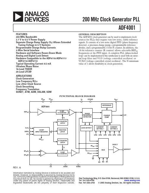
ADF4001
Parameter
B Version Unit
Test Conditions/Comments
RF CHARACTERISTICS (3 V) RF Input Frequency RF Input Sensitivity
5/165 –10/0
MHz min/max dBm min/max
See Figure 3 for Input Circuit
CHARGE PUMP ICP Sink/Source High Value Low Value Absolute Accuracy RSET Range ICP Three-State Leakage Current Sink and Source Current Matching ICP vs. VCP ICP vs. Temperature
Specifications subject to change without notice.
–2–
REV. A
ADF4001
TIMING CHARACTERISTICS (AVDD = DVDD = 3 V ؎ 10%, 5 V ؎ 10%; AVDD ≤ VP ≤ 6.0 V ; AGND = DGND = CPGND= 0 V;
REFERENCE
PHASE
FREQUENCY
CHARGE
CP
DETECTOR
PUMP
LOCK DETECT
CURRENT SETTING 1
CURRENT SETTING 2
CPI3 CPI2 CPI1 CPI6 CPI5 CPI4
AVDD SDOUT
MUX
HIGH Z
MUXOUT
REV. A
3D7324D-30资料
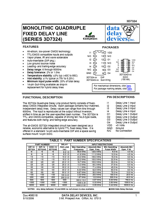
MONOLITHIC QUADRUPLEFIXED DELAY LINE(SERIES 3D7324)FEATURES• All-silicon, low-power CMOS technology• TTL/CMOS compatible inputs and outputs• Vapor phase, IR and wave solderable• Auto-insertable (DIP pkg.)• Low ground bounce noise• Leading- and trailing-edge accuracy• Delay range: 6 through 6000ns• Delay tolerance: 2% or 1.0ns• Temperature stability:±3% typ (-40C to 85C)• Vdd stability:±1% typical (4.75V to 5.25V)• Minimum input pulse width: 20% of total delay• 14-pin Gull-Wing available as drop-inreplacement for hybrid delay linesFUNCTIONAL DESCRIPTIONThe 3D7324 Quadruple Delay Line product family consists of fixed-delay CMOS integrated circuits. Each package contains four matched,independent delay lines. Delay values can range from 6ns through6000ns. The input is reproduced at the output without inversion,shifted in time as per the user-specified dash number. The 3D7324 isTTL- and CMOS-compatible, capable of driving ten 74LS-type loads,and features both rising- and falling-edge accuracy.The all-CMOS 3D7324 integrated circuit has been designed as areliable, economic alternative to hybrid TTL fixed delay lines. It isoffered in a standard 14-pin auto-insertable DIP and a space savingsurface mount 14-pin SOIC.PACKAGES1413121110981234567I1N/CI2I3I4N/CGNDVDDN/CO1N/CO2O3O43D7324-xx DIP3D7324G-xx Gull-Wing1234567141312111098I1N/CI2I3I4N/CGNDVDDN/CO1N/CO2O3O43D7324D-xxSOIC(150 Mil)PIN DESCRIPTIONSI1 Delay Line 1 InputI2 Delay Line 2 InputI3 Delay Line 3 InputI4 Delay Line 4 InputO1 Delay Line 1 OutputO2 Delay Line 2 OutputO3 Delay Line 3 OutputO4 Delay Line 4 OutputVDD +5VoltsGND GroundN/C NoConnection TABLE 1: PART NUMBER SPECIFICATIONSPART NUMBER DELAY INPUT RESTRICTIONSDIP-143D7324DIP-143D7324GSOIC-143D7324DPER LINE(ns)Max OperatingFrequencyAbsolute MaxOper. Freq.Min OperatingPulse WidthAbsolute MinOper. P.W.-6 -6 -6 6 ± 1.0 55.5 MHz 125.0 MHz 9.0 ns 4.0 ns-8 -8 -8 8 ± 1.0 41.6 MHz 111.0 MHz 12.0 ns 4.5 ns-10 -10 -10 10 ± 1.0 33.3 MHz 100.0 MHz 15.0 ns 5.0 ns-15 -15 -15 15 ± 1.0 22.2 MHz 100.0 MHz 22.5 ns 5.0 ns-20 -20 -20 20 ± 1.0 16.7 MHz 100.0 MHz 30.0 ns 5.0 ns-25 -25 -25 25 ± 1.0 13.3 MHz 83.3 MHz 37.5 ns 6.0 ns-30 -30 -30 30 ± 1.0 11.1 MHz 71.4 MHz 45.0 ns 7.0 ns-40 -40 -40 40 ± 1.0 8.33 MHz 62.5 MHz 60.0 ns 8.0 ns-50 -50 -50 50 ± 1.0 6.67 MHz 50.0 MHz 75.0 ns 10.0 ns -100 -100 -100 100 ± 2.0 3.33 MHz 25.0 MHz 150.0 ns 20.0 ns -200 -200 -200 200 ± 4.0 1.67 MHz 12.5 MHz 300.0 ns 40.0 ns -500 -500 -500 -500 500 ± 10.0 0.67 MHz 5.00 MHz 750.0 ns -1000 -1000 -1000 -1000 1000 ± 20 0.33 MHz 2.50 MHz 1500.0 ns -6000 -6000 -6000 -6000 6000 ±120 0.05 MHz 0.42 MHz 9000.0 ns NOTES: Any delay between 10 and 6000 ns not shown is also available. 2006 Data Delay DevicesAPPLICATION NOTESOPERATIONAL DESCRIPTIONThe 3D7324 quadruple delay line architecture is shown in Figure 1. The individual delay lines are composed of a number of delay cells connected in series. Each delay line produces at its output a replica of the signal present at its input, shifted in time. The delay lines are matched and share the same compensation signals, which minimizes line-to-line delay deviations over temperature and supply voltage variations.INPUT SIGNAL CHARACTERISTICSThe Frequency and/or Pulse Width (high or low) of operation may adversely impact the specified delay accuracy of the particular device. The reasons for the dependency of the output delay accuracy on the input signal characteristics are varied and complex. Therefore a Maximum and an Absolute Maximum operating inputfrequency and a Minimum and an Absolute Minimum operating pulse width have been specified.OPERATING FREQUENCYThe Absolute Maximum Operating Frequency specification, tabulated in Table 1, determines the highest frequency of the delay line input signal that can be reproduced, shifted in time at the device output, with acceptable duty cycle distortion.The Maximum Operating Frequencyspecification determines the highest frequency of the delay line input signal for which the output delay accuracy is guaranteed.To guarantee the Table 1 delay accuracy for input frequencies higher than the Maximum Operating Frequency , the 3D7324 must be tested at the user operating frequency.Therefore, to facilitate production and device identification, the part number will include a custom reference designator identifying the intended frequency of operation. Theprogrammed delay accuracy of the device is guaranteed, therefore, only at the user specified input frequency. Small input frequency variation about the selected frequency will only marginally impact the programmed delay accuracy, if at all. Nevertheless, it is strongly recommended that the engineering staff at DATA DELAY DEVICES be consulted.OPERATING PULSE WIDTHThe Absolute Minimum Operating Pulse Width (high or low) specification, tabulated in Table 1, determines the smallest Pulse Width of the delay line input signal that can bereproduced, shifted in time at the device output, with acceptable pulse width distortion.The Minimum Operating Pulse Width (high or low) specification determines the smallest Pulse Width of the delay line input signal for which the output delay accuracy tabulated in Table 1 is guaranteed.To guarantee the Table 1 delay accuracy for input pulse width smaller than the Minimum Operating Pulse Width , the 3D7324 must be tested at the user operating pulse width. Therefore, to facilitate production and device identification, the part number will include aO1I1 Dela y Dela y Dela y Dela yO2I2O3I3O4I4Temp & VDD Compensatio VDDGND Figure 1: 3D7324 Functional DiagramAPPLICATION NOTES (CONT’D)custom reference designator identifying the intended frequency and duty cycle of operation. The programmed delay accuracy of the device is guaranteed, therefore, only for the user specified input characteristics. Small input pulse width variation about the selected pulse width will only marginally impact the programmed delay accuracy, if at all. Nevertheless, it is strongly recommended that the engineering staff at DATA DELAY DEVICES be consulted. POWER SUPPLY AND TEMPERATURE CONSIDERATIONS The delay of CMOS integrated circuits is strongly dependent on power supply and temperature. The monolithic 3D7324 programmable delay line utilizes novel and innovative compensation circuitry to minimize the delay variations induced by fluctuations in power supply and/or temperature.The thermal coefficient is reduced to 300 PPM/C, which is equivalent to a variation , over the -40C to 85C operating range, of ±3% from the room-temperature delay settings and/or1.0ns, whichever is greater. The power supply coefficient is reduced, over the 4.75V to 5.25V operating range, to ±1% of the delay settings at the nominal 5.0VDC power supply and/or2.0ns, whichever is greater. It is essential that the power supply pin be adequately bypassed and filtered. In addition, the power bus should be of as low an impedance construction as possible. Power planes are preferred.DEVICE SPECIFICATIONSTABLE 2: ABSOLUTE MAXIMUM RATINGSPARAMETER SYMBOL MIN MAXUNITSNOTES DC Supply Voltage V DD -0.3 7.0 VInput Pin Voltage V IN -0.3V DD+0.3 VInput Pin Current I IN -1.0 1.0 mA25C Storage Temperature T STRG -55 150 CLead Temperature T LEAD300 C10secTABLE 3: DC ELECTRICAL CHARACTERISTICS(-40C to 85C, 4.75V to 5.25V)PARAMETER SYMBOLMINMAXUNITSNOTES Static Supply Current* I DD 5mA High Level Input Voltage V IH 2.0 VLow Level Input Voltage V IL0.8V High Level Input Current I IH -1 1 µA V IH = V DDLow Level Input Current I IL -1 1 µA V IL = 0VHigh Level Output Current I OH-4.0mAV DD = 4.75VV OH = 2.4V Low Level Output Current I OL 4.0 mAV DD = 4.75VV OL = 0.4V Output Rise & Fall Time T R & T F 2 ns C LD = 5 pf*I DD(Dynamic) = 4 * C LD * V DD * F Input Capacitance = 10 pf typical where: C LD = Average capacitance load/line (pf) Output Load Capacitance (C LD) = 25 pf maxF = Input frequency (GHz)SILICON DELAY LINE AUTOMATED TESTINGTEST CONDITIONSINPUT: OUTPUT:Ambient Temperature: 25o C ± 3oC R load : 10K Ω ± 10%Supply Voltage (Vcc): 5.0V ± 0.1V C load : 5pf± 10% Input Pulse: High = 3.0V ± 0.1V Threshold: 1.5V (Rising & Falling) Low = 0.0V ± 0.1V Source Impedance: 50Ω Max. 10K Ω470Ω5pfDevice Under Test Digital Scope Rise/Fall Time: 3.0 ns Max. (measuredbetween 0.6V and 2.4V ) Pulse Width: PW IN = 1.25 x Total DelayPeriod: PER IN = 2.5 x Total DelayNOTE: The above conditions are for test only and do not in any way restrict the operation of the device.Figure 2: Test SetupFigure 3: Timing Diagramt PLHt PHLPER INPW INt RISEt FALL0.6V0.6V1.5V 1.5V2.4V 2.4V 1.5V1.5VV IHV ILV OHV OLINPUT SIGNALOUTPUT SIGNAL。
QN8035pdf

players. It integrates FM receive functions, auto-seek and clear channel scan. Advanced digital architecture enables
superior receiver sensitivity and crystal clear audio.
Confidential Information contained herein is covered under Non-Disclosure Agreement (NDA).
Advance Technical Information. This is a product under development. Characteristics and specifications are subject to change without notice.
• Robust Operation • -250C to +850C operation • ESD protection on all input and output pads
• 1 KHz Tone Generator Inside
, ___________________________ Typical Applications ________________________
4
QQ: Control Interface Protocol .............................................................................................................................14
ADF4153资料
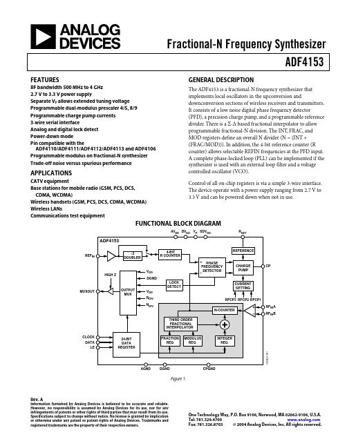
Fractional-N Frequency SynthesizerADF4153Rev. AInformation furnished by Analog Devices is believed to be accurate and reliable. However, no responsibility is assumed by Analog Devices for its use, nor for any infringements of patents or other rights of third parties that may result from its use. Specifications subject to change without notice. No license is granted by implication or otherwise under any patent or patent rights of Analog Devices. Trademarks and registered trademarks are the property of their respective owners.One Technology Way, P.O. Box 9106, Norwood, MA 02062-9106, U.S.A. Tel: 781.329.4700 Fax: 781.326.8703© 2004 Analog Devices, Inc. All rights reserved.FEATURESRF bandwidth 500 MHz to 4 GHz 2.7 V to 3.3 V power supplySeparate V P allows extended tuning voltage Programmable dual-modulus prescaler 4/5, 8/9 Programmable charge pump currents 3-wire serial interfaceAnalog and digital lock detect Power-down modePin compatible with theADF4110/ADF4111/ADF4112/ADF4113 and ADF4106 Programmable modulus on fractional-N synthesizer Trade-off noise versus spurious performanceAPPLICATIONSCATV equipmentBase stations for mobile radio (GSM, PCS, DCS, CDMA, WCDMA)Wireless handsets (GSM, PCS, DCS, CDMA, WCDMA) Wireless LANsCommunications test equipmentGENERAL DESCRIPTIONThe ADF4153 is a fractional-N frequency synthesizer that implements local oscillators in the upconversion anddownconversion sections of wireless receivers and transmitters. It consists of a low noise digital phase frequency detector(PFD), a precision charge pump, and a programmable reference divider. There is a Σ-Δ based fractional interpolator to allow programmable fractional-N division. The INT, FRAC, and MOD registers define an overall N divider (N = (INT + (FRAC/MOD))). In addition, the 4-bit reference counter (R counter) allows selectable REFIN frequencies at the PFD input. A complete phase-locked loop (PLL) can be implemented if the synthesizer is used with an external loop filter and a voltage controlled oscillator (VCO).Control of all on-chip registers is via a simple 3-wire interface. The device operate with a power supply ranging from 2.7 V to 3.3 V and can be powered down when not in use.FUNCTIONAL BLOCK DIAGRAMDATALECLOCK REF ININ A IN BMUXOUTFigure 1.ADF4153Rev. A | Page 2 of 24TABLE OF CONTENTSSpecifications.....................................................................................3 Timing Characteristics.....................................................................5 Absolute Maximum Ratings............................................................6 ESD Caution..................................................................................6 Pin Configuration and Pin Function Descriptions......................7 Typical Performance Characteristics.............................................8 Circuit Description.........................................................................10 Reference Input Section.............................................................10 RF Input Stage.............................................................................10 RF INT Divider...........................................................................10 INT, FRAC, MOD, and R Relationship....................................10 RF R COUNTER........................................................................10 Phase Frequency Detector (PFD) and Charge Pump............11 MUXOUT and LOCK Detect...................................................11 Input Shift Registers...................................................................11 Program Modes..........................................................................11 N Divider Register, R0...............................................................17 R Divider Register, R1................................................................17 Control Register, R2...................................................................17 Noise and Spur Register, R3......................................................18 Reserved Bits...............................................................................18 RF Synthesizer: A Worked Example........................................18 Modulus.......................................................................................19 Reference Doubler and Reference Divider.............................19 12-Bit Programmable Modulus................................................19 Spurious Optimization and Fastlock.......................................19 Phase Resync and Spur Consistency.......................................19 Spurious Signals—Predicting Where They Will Appear.......20 Filter Design—ADIsimPLL.......................................................20 Interfacing...................................................................................20 PCB Design Guidelines for Chip Scale Package....................21 Outline Dimensions.......................................................................22 Ordering Guide.. (22)REVISION HISTORY1/04—Data Sheet Changed from a REV . 0 to a REV . ARenumbered Figures and Tables..............................UNIVERSAL Changes to Specifications...............................................................3 Changes to Pin Function Description..........................................7 Changes to RF Power-Down section..........................................17 Changes to PCB Design Guidelines for Chip ScalePackage section..............................................................................21 Updated Outline Dimensions......................................................22 Updated Ordering Guide..............................................................22 7/03—Revision 0: Initial VersionADF4153Rev. A | Page 3 of 24SPECIFICATIONS 1AV DD = DV DD = SDV DD = 2.7 V to 3.3 V; V P = AV DD to 5.5 V; AGND = DGND = 0 V; T A = T MIN to T MAX , unless otherwise noted; dBm referred to 50 Ω. Table 1.Parameter B Version Unit Test Conditions/Comments RF CHARACTERISTICS (3 V)See Figure 17 for input circuit. RF Input Frequency (RF IN )20.5/4.0 G Hz min/max −8 dBm/0 dBm min/max. For lower frequencies,ensure slew rate (SR) > 396 V/µs.1.0/4.0 GHz min/max −10 dBm/0 dBm min/max. REFERENCE CHARACTERISTICS See Figure 16 for input circuit. REF IN Input Frequency 2 10/250 MHz min/max For f < 10 MHz, use a dc-coupled CMOS compatiblesquare wave, slew rate > 21 V/µs.REF IN Input Sensitivity 0.7/AV DD V p-p min/max AC-coupled. 0 to AV DD V max CMOS compatible. REF IN Input Capacitance 10 pF max REF IN Input Current ±100 µA max PHASE DETECTORPhase Detector Frequency 332 MHz max CHARGE PUMP I CP Sink/Source Programmable. See Table 5. High Value 5 mA typ With R SET = 5.1 kΩ. Low Value 312.5 µA typ Absolute Accuracy 2.5 % typ With R SET = 5.1 kΩ. R SET Range 1.5/10 kΩ min/max I CP Three-State Leakage Current 1 nA typ Sink and source current. Matching 2 % typ 0.5 V < V CP < V P – 0.5. I CP vs. V CP 2 % typ 0.5 V < V CP < V P – 0.5. I CP vs. Temperature 2 % typ V CP = V P /2. LOGIC INPUTS V INH , Input High Voltage 1.4 V min V INL , Input Low Voltage 0.6 V max I INH /I INL , Input Current ±1 µA max C IN , Input Capacitance 10 pF max LOGIC OUTPUTS V OH , Output High Voltage 1.4 V min Open-drain 1 kΩ pull-up to 1.8 V. V OL , Output Low Voltage 0.4 V max I OL = 500 µA. POWER SUPPLIES AV DD 2.7/3.3 V min/V max DV DD , SDV DD AV DD V P AV DD /5.5 V min/V max I DD 4 24 mA max 20 mA typical. Low Power Sleep Mode 1 µA typ NOISE CHARACTERISTICSPhase Noise Figure of Merit 5−217 dBc/Hz typ ADF4153 Phase Noise Floor 6 −147 dBc/Hz typ @ 10 MHz PFD frequency. −143 dBc/Hz typ @ 26 MHz PFD frequency. Phase Noise Performance 7 @ VCO output.1750 MHz Output 8−106 dBc/Hz typ @ 1 kHz offset, 26 MHz PFD frequency.See footnotes on next page.ADF41531 Operating temperature is B version: −40°C to +80°C.2 Use a square wave for frequencies below f MIN.3 Guaranteed by design. Sample tested to ensure compliance.4 AC coupling ensures AV DD/2 bias. See Figure 16 for typical circuit.5 This figure can be used to calculate phase noise for any application. Use the formula –217 + 10log(f PFD) + 20logN to calculate in-band phase noise performance as seen at the VCO output. The value given is the lowest noise mode.6 The synthesizer phase noise floor is estimated by measuring the in-band phase noise at the output of the VCO and subtracting 20logN (where N is the N divider value). The value given is the lowest noise mode.7 The phase noise is measured with the EVAL-ADF4153EB1 evaluation board and the HP8562E spectrum analyzer.8 f REFIN = 26 MHz; f PFD = 10 MHz; offset frequency = 1 kHz; RF OUT = 1750 MHz; N = 175; loop B/W = 20 kHz; lowest noise mode.Rev. A | Page 4 of 24ADF4153Rev. A | Page 5 of 24TIMING CHARACTERISTICS 1AV DD = DV DD = SDV DD = 2.7 V to 3.3 V; V P = AV DD to 5.5 V; AGND = DGND = 0 V; T A = T MIN to T MAX , unless otherwise noted; dBm referred to 50 Ω. Table 2.Parameter Limit at T MIN to T MAX (B Version) Unit Test Conditions/Comments t 1 20 ns min LE Setup Timet 2 10 ns min DATA to CLOCK Setup Time t 3 10 ns min DATA to CLOCK Hold Time t 4 25 ns min CLOCK High Duration t 5 25 ns min CLOCK Low Duration t 6 10 ns min CLOCK to LE Setup Time t 720 ns min LE Pulse Width1Guaranteed by design but not production tested.CLOCKDATALELEFigure 2. Timing DiagramADF4153Rev. A | Page 6 of 24ABSOLUTE MAXIMUM RATINGS 1, 2, 3, 4T A = 25°C, unless otherwise noted. Table 3.Parameter Rating V DD to GND −0.3 V to +4 V V DD to V DD −0.3 V to +0.3 V V P to GND −0.3 V to +5.8 V V P to V DD −0.3 V to +5.8 V Digital I/O Voltage to GND −0.3 V to V DD + 0.3 V Analog I/O Voltage to GND −0.3 V to V DD + 0.3 V REF IN , RF IN to GND −0.3 V to V DD + 0.3 V Operating Temperature Range Industrial (B Version) −40°C to +85°C Storage Temperature Range −65°C to +150°C Maximum Junction Temperature 150°C TSSOP θJA Thermal Impedance 150.4°C/W LFCSP θJA Thermal Impedance (Paddle Soldered) 122°C/W LFCSP θJA Thermal Impedance (Paddle Not Soldered) 216°C/W Lead Temperature, Soldering Vapor Phase (60 sec) 215°CInfrared 220°C1Stresses above those listed under Absolute Maximum Ratings may cause permanent damage to the device. This is a stress rating only; functional operation of the device at these or any other conditions above those listed in the operational sections of this specification is not implied. Exposure to absolute maximum rating conditions for extended periods may affect device reliability. 2This device is a high performance RF integrated circuit with an ESD rating of < 2 kV, and it is ESD sensitive. Proper precautions should be taken for handling and assembly. 3GND = AGND = DGND = 0 V. 4V DD = AV DD = DV DD = SDV DD .ESD CAUTIONESD (electrostatic discharge) sensitive device. Electrostatic charges as high as 4000 V readily accumulate on the human body and test equipment and can discharge without detection. Although this product features proprietary ESD protection circuitry, permanent damage may occur on devices subjected to high energy electrostatic discharges. Therefore, proper ESD precautions are recommended to avoid performance degradation or loss of functionality.ADF4153Rev. A | Page 7 of 24PIN CONFIGURATION AND PIN FUNCTION DESCRIPTIONSAGND RF IN B RFI IN A AV DD REF IN LEDATACLK SDV DDDGNDR SET CP CPGND V P DV DDMUXOUT03685-A -002Figure 3. TSSOP Pin Configuration03685-A -00315141312CPGND1AGND 2AGND 3C P 11MUXOUT LE DATA CLK SDV DDA V D D 6A V D D 7R E F I N 8D G N D 9D G N D 10RF IN B 4RF IN A5R S E T V P D V D D D V D D1820191716Figure 4. LFCSP Pin ConfigurationADF4153Rev. A | Page 8 of 24TYPICAL PERFORMANCE CHARACTERISTICSFigure 5 to Figure 10: RF OUT = 1.722 GHz, PFD Freq = 26 MHz, INT = 66, Channel Spacing = 200 kHz, Modulus = 130, Fraction = 1/130, and I CP = 5 mA.Loop Bandwidth = 20 kHz, Reference = Fox 10 MHz TCXO, VCO = Vari-L VCO190-1750T, Eval Board = Eval-ADF4153EB1, measurements taken on HP8562E spectrum analyzer.O U T P U T P O W E R (d B )0–30–50–80–90–100–60–70–40–20–10–2kHz–1kHz1kHz2kHz1.722GHz03685-A -004Figure 5. Phase Noise (Lowest Noise Mode)O U T P U T P O W E R (d B )0–30–50–80–60–70–40–20–10–2kHz –1kHz 1kHz 2kHz1.722GHz 03685-A -005Figure 6. Phase Noise (Low Noise Mode and Spur Mode)O U T P U T P O W E R (d B )0–30–50–80–90–100–60–70–40–20–10–2kHz–1kHz1kHz2kHz1.722GHz03685-A -006Figure 7. Phase Noise (Lowest Spur Mode) O U T P U T P O W E R (d B )–30–50–80–90–60–70–40–20–10–400kHz–200kHz200kHz400kHz1.722GHz–10003685-A -007Figure 8. Spurs (Lowest Noise Mode)O U T P U T P O W E R (d B )0–30–50–80–90–100–60–70–40–20–10–400kHz–200kHz200kHz400kHz1.722GHz03685-A -008Figure 9. Spurs (Low Noise and Spur Mode)O U T P U T P O W E R (d B )0–30–50–80–90–100–60–70–40–20–10V DD = 3V, V P = 5V I CP = 5mAPFD FREQUENCY = 26MHz CHANNEL STEP = 200kHz LOOP BANDWIDTH = 20kHz LOWEST SPUR NOISE N = 66 1/130 RBW = 10HzREFERENCELEVEL =–4.2dBm–400kHz–200kHz200kHz400kHz1.722GHz03685-A -009Figure 10. Spurs (Lowest Spur Mode)ADF4153Rev. A | Page 9 of 24P H A S E N O I S E (d B c /H z )PHASE DETECTOR FREQUENCY (kHz)–130–140–150–160–17010010001000010000003685-A -010Figure 11. PFD Noise Floor vs. PFD Frequency (Lowest Noise Mode)FREQUENCY (GHz)A M P L I T U D E (dB m )50–5–10–20–15–25–30–3503685-A -011Figure 12. RF Input SensitivityV CP (V)60–6I C P (m A )42–2–4–5–3–11350123453685-A -012Figure 13. Charge Pump Output CharacteristicsR SET VALUE (k Ω)–80–85–11003530252015105P H A S E N O I S E (d B c /H z )–90–95–105–10003685-A -013Figure 14. Phase Noise vs. R SETTEMPERATURE(°C)–90–94–104–60100–40P H A S E N O I S E (d B c /H z )–200204060–96–98–92–102–1008003685-A -014Figure 15. Phase Noise vs. TemperatureADF4153Rev. A | Page 10 of 24CIRCUIT DESCRIPTIONREFERENCE INPUT SECTIONThe reference input stage is shown in Figure 16. SW1 and SW2 are normally closed switches. SW3 is normally open. When power-down is initiated, SW3 is closed and SW1 and SW2 are opened. This ensures that there is no loading of the REF IN pin on power-down.04414-0-010POWER-DOWNFigure 16. Reference Input StageRF INPUT STAGEThe RF input stage is shown in Figure 17. It is followed by a 2-stage limiting amplifier to generate the current mode logic (CML) clock levels needed for the prescaler.RF IN RF IN 03Figure 17. RF Input StageRF INT DIVIDERThe RF INT CMOS counter allows a division ratio in the PLL feedback counter. Division ratios from 31 to 511 are allowed.INT, FRAC, MOD, AND R RELATIONSHIPThe INT, FRAC, and MOD values, in conjunction with the R counter, make it possible to generate output frequencies that are spaced by fractions of the phase frequency detector (PFD). See the RF Synthesizer: A Worked Example section for more information. The RF VCO frequency (RF OUT ) equation is()()MOD FRAC INT F RF PFD OUT +×= (1) where RF OUT is the output frequency of external voltage controlled oscillator (VCO).()R D REF F IN PFD +×=1 (2)where:REF IN is the reference input frequency. D is the REF IN doubler bit.R is the preset divide ratio of binary 4-bit programmable reference counter (1 to 15).INT is the preset divide ratio of binary 9-bit counter (31 to 511).MOD is the preset modulus ratio of binary 12-bit programmable FRAC counter (2 to 4095). FRAC is the preset fractional ratio of binary 12-bit programmable FRAC counter (0 to MOD).RF R COUNTERThe 4-bit RF R counter allows the input reference frequency (REF IN ) to be divided down to produce the reference clock to the PFD. Division ratios from 1 to 15 are allowed.03685-A -016Figure 18. A and B CountersPHASE FREQUENCY DETECTOR (PFD) AND CHARGE PUMPThe PFD takes inputs from the R counter and N counter and produces an output proportional to the phase and frequency difference between them. Figure 19 is a simplified schematic. The PFD includes a fixed delay element that sets the width of the antibacklash pulse, which is typically 3 ns. This pulseensures that there is no dead zone in the PFD transfer function, and gives a consistent reference spur level.CP–IN+IN03685-A -017Figure 19. PFD Simplified SchematicMUXOUT AND LOCK DETECTThe output multiplexer on the ADF4153 allows the user toaccess various internal points on the chip. The state of MUXOUT is controlled by M3, M2, and M1 (see Table 8).Figure 20 shows the MUXOUT section in block diagram form. The N-channel open-drain analog lock detect should be operated with an external pull-up resistor of 10 kΩ nominal.When lock has been detected, it is high with narrow low-going pulses.DGNDMUXOUTDV 03685-A -018Figure 20. MUXOUT SchematicINPUT SHIFT REGISTERSThe ADF4153 digital section includes a 4-bit RF R counter, a 9-bit RF N counter, a 12-bit FRAC counter, and a 12-bit modulus counter. Data is clocked into the 24-bit shift register on each rising edge of CLK. The data is clocked in MSB first. Data is transferred from the shift register to one of four latches on the rising edge of LE. The destination latch is determined by the state of the two control bits (C2 and C1) in the shift register. These are the 2 LSBs, DB1 and DB0, as shown in Figure 2. The truth table for these bits is shown in Table 5. Table 6 shows a summary of how the latches are programmed.PROGRAM MODESTable 5 through Table 10 show how to set up the program modes in the ADF4153.The ADF4153 programmable modulus is double buffered. This means that two events have to occur before the part uses a new modulus value. First, the new modulus value is latched into the device by writing to the R divider register. Second, a new write must be performed on the N divider register. Therefore, any time that the modulus value has been updated, the N divider register must be written to after this, to ensure that the modulus value is loaded correctly. Table 5. C2 and C1 Truth TableControl BitsC2 C1 Register 0 0 N Divider Register 0 1 R Divider Register 1 0 Control Register 1 1 Noise and Spur RegisterTable 6. Register Summary03685-A -019Table 7. N Divider Register Map3Table 8. R Divider Register MapTable 9. Control Register MapTable 10. Noise and Spur RegisterN DIVIDER REGISTER, R0With R0[1, 0] set to [0, 0], the on-chip N divider register is programmed. Table 7 shows the input data format for programming this register.9-Bit INT ValueThese nine bits control what is loaded as the INT value. This is used to determine the overall feedback division factor. It is used in Equation 1.12-Bit FRAC ValueThese 12 bits control what is loaded as the FRAC value into the fractional interpolator. This is part of what determines the overall feedback division factor. It is used in Equation 1. The FRAC value must be less than or equal to the value loaded into the MOD register.FastlockWhen set to logic high, this enables the fastlock. This sets the charge pump current to its maximum value. When set to logic low, the charge pump current is equal to the value programmed in the function register.R DIVIDER REGISTER, R1With R1[1, 0] set to [0, 1], the on-chip R divider register is programmed. Table 8 shows the input data format for programming this register.Load ControlWhen set to logic high, the value being programmed in the modulus is not loaded into the modulus. Instead, it sets the resync delay of the Σ-Δ. This is done to ensure phase resync when changing frequencies. See the Phase Resync and Spur Consistency section for more information and a worked example.MUXOUTThe on-chip multiplexer is controlled by R1[22 ... 20] on the ADF4153. Table 8 shows the truth table.Digital Lock DetectThe digital lock detect output goes high if there are 40 successive PFD cycles with an input error of less than 15 ns. It stays high until a new channel is programmed or until the error at the PFD input exceeds 30 ns for one or more cycles. If the loop bandwidth is narrow compared to the PFD frequency, the error at the PFD inputs may drop below 15 ns for 40 cycles around a cycle slip. Therefore, the digital lock detect may go falsely high for a short period until the error again exceeds30 ns. In this case, the digital lock detect is reliable only as a loss-of-lock detector.Prescaler (P/P + 1)The dual-modulus prescaler (P/P + 1), along with the INT, FRAC, and MOD counters, determines the overall division ratio from the RF IN to the PFD input. Operating at CML levels, it takes the clock from the RF input stage and divides it down for the counters. It is based on a synchronous 4/5 core. When set to 4/5, the maximum RF frequency allowed is 2 GHz. Therefore, when operating the ADF4153 above 2 GHz, this must be set to 8/9. The prescaler limits the INT value.With P = 4/5, N MIN = 31.With P = 8/9, N MIN = 91.The prescaler can also influence the phase noise performance. If INT < 91, a prescaler of 4/5 should be used. For applications where INT > 91, P = 8/9 should be used for optimum noise performance (see Table 8).4-Bit RF R CounterThe 4-bit RF R counter allows the input reference frequency (REF IN) to be divided down to produce the reference clock to the phase frequency detector (PFD). Division ratios from 1 to 15 are allowed.12-Bit Interpolator ModulusThis programmable register sets the fractional modulus. This is the ratio of the PFD frequency to the channel step resolution on the RF output. Refer to the RF Synthesizer: A Worked Example section for more information.The ADF4153 programmable modulus is double buffered. This means that two events have to occur before the part uses a new modulus value. First, the new modulus value is latched into the device by writing to the R divider register. Second, a new write must be performed on the N divider register. Therefore, any time that the modulus value has been updated, the N divider register must be written to after this, to ensure that the modulus value is loaded correctly.CONTROL REGISTER, R2With R2[1, 0] set to [0, 1], the on-chip control register is programmed. Table 9 shows the input data format for programming this register.RF Counter ResetDB3 is the RF counter reset bit for the ADF4153. When this is 1, the RF synthesizer counters are held in reset. For normal operation, this bit should be 0.RF Charge Pump Three-StateThis bit puts the charge pump into three-state mode when programmed to 1. It should be set to 0 for normal operation. RF Power-DownDB4 on the ADF4153 provides the programmable power-down mode. Setting this bit to 1 performs a power-down. Setting this bit to 0 returns the synthesizer to normal operation. While in software power-down mode, the part retains all information in its registers. Only when supplies are removed are the register contents lost.When a power-down is activated, the following events occur:1. All active dc current paths are removed.2. The synthesizer counters are forced to their load stateconditions.3. The charge pump is forced into three-state mode.4. The digital lock detect circuitry is reset.5. The RF IN input is debiased.6. The input register remains active and capable of loadingand latching data.Lock Detect Precision (LDP)When this bit is programmed to 0, three consecutive reference cycles of 15 ns must occur before digital lock detect is set. When this bit is programmed to 1, five consecutive reference cycles of 15 ns must occur before digital lock detect is set.Phase Detector PolarityDB6 in the ADF4153 sets the phase detector polarity. When the VCO characteristics are positive, this should be set to 1. When they are negative, it should be set to 0.Charge Pump Current SettingDB7, DB8, and DB9 set the charge pump current setting. This should be set to the charge pump current that the loop filter is designed with (see Table 9).REF IN DoublerSetting this bit to 0 feeds the REF IN signal directly to the 4-bit RF R counter, disabling the doubler. Setting this bit to 1 multiplies the REF IN frequency by a factor of 2 before feeding into the 4-bit R counter. When the doubler is disabled, the REF IN falling edge is the active edge at the PFD input to the fractional synthesizer. When the doubler is enabled, both the rising and falling edges of REF IN become active edges at the PFD input. When the doubler is enabled and the lowest spur mode is chosen, the in-band phase noise performance is sensitive to the REF IN duty cycle. The phase noise degradation can be as much as 5 dB for the REF IN duty cycles outside a 45% to 55% range. The phase noise is insensitive to the REF IN duty cycle in the lowest noise mode and in the lowest noise and spur mode. The phase noise is insensitive to REF IN duty cycle when the doubler is disabled.NOISE AND SPUR REGISTER, R3With R3[1, 0] set to 1, 1, the on-chip noise and spur register is programmed. Table 10 shows the input data format for programming this register.Noise and Spur ModeNoise and spur mode allows the user to optimize a design either for improved spurious performance or for improved phase noise performance. When the lowest spur setting is chosen, dither is enabled. This randomizes the fractional quantizationnoise so that it looks more like white noise rather than spuriousnoise. This means that the part is optimized for improvedspurious performance. This operation would normally be usedwhen the PLL closed-loop bandwidth is wide, for fast-lockingapplications. (Wide-loop bandwidth is seen as a loop bandwidthgreater than 1/10 of the RF OUT channel step resolution (f RES)). Awide-loop filter does not attenuate the spurs to a level that anarrow-loop bandwidth would. When the low noise and spursetting is enabled, dither is disabled. This optimizes thesynthesizer to operate with improved noise performance.However, the spurious performance is degraded in this modecompared to the lowest spurs setting. To further improve noiseperformance, the lowest noise setting option can be used, whichreduces the phase noise. As well as disabling the dither, it alsoensures that the charge pump is operating in an optimumregion for noise performance. This setting is extremely usefulwhere a narrow-loop filter bandwidth is available. Thesynthesizer ensures extremely low noise and the filter attenuatesthe spurs. The typical performance characteristics give the useran idea of the trade-off in a typical WCDMA setup for thedifferent noise and spur settings.RESERVED BITSThese bits should be set to 0 for normal operation.RF SYNTHESIZER: A WORKED EXAMPLEThis equation governs how the synthesizer should beprogrammed.()[][]PFDOUTFMODFRACINTRF×+= (3)where:RF OUT is the RF frequency output.INT is the integer division factor.FRAC is the fractionality.MOD is the modulus.()[]RDREFF INPFD+×=1 (4) where:REF IN is the reference frequency input.D is the RF REF IN doubler bit.R is the RF reference division factor.。
德州仪器2010年军品指南

10
Defense Digital Signal Processors (DSPs) . . . . . . . . . . . . . . . . . . . . 13 军用数字信号处理器 (DSP) 13
2010
军用产品 Defense
➔ 概述及目录 Overview and Contents
德州仪器高可靠性军工与航天 (TI HiRel) 产 The Texas Instruments High Reliability 品部( CAGE 编号为 01295 )成立于 1978 Defense & Aerospace (TI HiRel) Group 年,是专为满足军工客户的特殊需求而成 (CAGE code number 01295) was
SMJ320C40: Floating-Point Digital Signal Processor . . . . . . . . . . . . . . . . . . . . . .5 5 SMJ320C40: 浮点型数字信号处理器
created in 1978 to serve the special 立的。如今,作为 TI 公司旗下的一个专门 requirements of the defense customer. 的业务部门, TI HiRel已经成为世界最大的
This position enables us to leverage the latest technology, manufacturHiRel专门针对那些要求具有可靠性、合格 ing capability and product mix for 证、供应商明细图 (VID) 、标准微电路制 advanced and critical aerospace and 图 (SMD) 和基线控制等特殊需求提供了广 defense applications. TI HiRel offers 阔的选择,如半导体技术、代工服务、组 a broad selection of semiconductor technology, foundry services, compo件、先进的包装及技术支持。 nents, advanced packaging and support for specific requirements where TI的HiRel产品组合所提供的器件,如增强 reliability, qualification, vendor item 型产品 (EP),具有两种封装类型:塑料封 drawings (VIDs), standard microcircuit 装和具有扩展工作温度范围的完全的军规 drawings (SMDs) and baseline control 级陶瓷 (QML) 封装。我们还提供 QML Q are critical.
low drop-out voltage regulators cap-less architecture comparison!
Digital Object Identifier 10.1109/MCAS.2014.2314263Date of publication: 20 May 2014Low Drop-Out Voltage Regulators: Capacitor-less Architecture ComparisonJoselyn torres, mohamed El-nozahi,ahmed amer, seenu gopalraju, reza abdullah, Kamran Entesari,and Edgar sánchez-sinencioAbstractI. IntroductionLow drop-out (LDO) voltage regulators are essential building blocks in power-management systems. Power-management systems for microprocessors and portable devices often use multiple LDO regulatorsto provide a regulated supply voltage with minimal rip-ple to supply-noise-sensitive blocks. The conventional LDO regulator block diagram is shown in Fig. 1(a) and it consists of a pass transistor ,M P an error amplifier EA, a feedback network (R F 1 and ),R F 2 and a bulky off-chip capacitor .C L Current source I L represents the required current by the load. The off-chip capacitor is used to achieve stability and good transient response,demand for system-on-chip solutions has increased the interest in low drop-out (Ldo) voltage regulators which do not require a bulky off-chip capacitor to achieve stability, also called capacitor-less Ldo (cL-Ldo) regulators. several architectures have been proposed; however comparing these reported architectures proves difficult, as each has a distinct process technology and specifications. this paper compares cL-Ldos in a unified matter. We designed, fabricated, and tested five illustrative cL-Ldo regulator topologies under common design conditions using 0.6µm cmos technol-ogy. We compare the architectures in terms of (1) line/load regulation, (2) power supply rejection, (3) line/load transient, (4) total on-chip compensation capacitance, (5) noise, and (6) quiescent power con-sumption. Insights on what optimal topology to choose to meet particular Ldo specifications are provided.ImagE by dr. E. sanchEz-sInEncIo.Joselyn Torres, Kamran Entesari, and Edgar Sánchez- ‐Sinencio are with Texas A&M University, College Station, TX, USA. Mohamed El- ‐Nozahi is with Ain Shams University, Cairo, Egypt. Ahmed Amer, Seenu Gopalraju, and Reza Abdullah are with Texas Instruments Inc., USA.and its value is often in the order of several micro-farads. However, this off-chip capacitor increases the total cost of the system and precludes the LDO regulator to be used in system-on-chip solutions. Hence, a LDO regula-tor that does not require an off-chip capacitor can signif-icantly reduce the number of external components and PCB area, thereby reducing the total cost of the system. This type of LDO regulators are known as capacitor-less LDOs (CL-LDOs) in the literature and its block diagram is shown in Fig. 1(b). In Fig. 1(b), C L models the parasitic capacitors and/or any integrated capacitor at the out-put node. C L is typically in the order of pico-farads in CL-LDO regulators.Previous works have been designed for different system requirements and implemented in different fab-rication technologies. As a result, comparing their per-formance proves difficult. In this work, we designed, fabricated, and measured five different CL-LDO regula-tors in the same process (0.6µm CMOS) under com-mon design specifications to facilitate comparison. Our remarks and observations are suitable for the chosen design constraints.Section II discusses the design issues in CL-LDO regulators. Representative CL-LDO regulator topologies [1]–[5], [15]–[32] are presented in Sections III and IV . Remarks on CL-LDO regulator architectures and experi-mental results are presented in Section V . Conclusions are drawn in Section VI.II. Design ConsiderationsKey design considerations for CL-LDO regulators include: stability at very light loads (low ),I L line/load regulation, line/load transient, and power supply rejec-tion ().PSR Trade-offs between these parameters are often topology dependent. A brief introduction to these design considerations is introduced in this section.A. StabilityA CL-LDO regulator model for stability analysis is shown in Fig. 2. This model uses Fig. 1(b) as reference. Signals ,V IN ,V OUT and V REF represent the input, output, and ref-erence voltages, respectively. b is the feedback factor set by the /,R R R F F F 221+^h and A p is the pass-transistorOn-ChipOn-Chip V REFV REFV OUTV INV INR F1I LC LI LC LR F2R F1R F2V INM PC 1C 2ωp1V INM PC 1ωp1ωp 0V OUTC 2ωp 0EA LoopLoop+–EA+–Dominant PoleDominant Pole(a)(b)Figure 1. (a) conventional Ldo regulator and (b) cL-Ldo regulator.V IN V V REF++––∑∑Error AmplifierA EA (s )A p 1 + s / poPass Transistor & LoadFeedback Factor cL-Ldo regulator model for stability analysis.voltage gain. The error amplifier transfer function isrepresented by A sEA ^h and can be expressed as, //,/,A sss A s A 111for two stage EA for one stage EA ,,p p op o121EA EA EA --~~~=+++^^^h h h Z [\]]]], (1)where po ~ is the output pole of the system and is given by the C L and the parallel combination of the output resis-tance of the pass transistor /,g 1ds ^h load resistance /,g 1L ^h and feedback resistors /.g 1b ^h The EA DC gain is repre-sented by ,A ,o EA and p 1~ and p 2~ are the dominant and non-dominant poles of the error amplifier, respectively.Stability is a critical design criterion since the unity gain frequency UGF ^h and location of the poles vary significantly with the load current condition, I L [6]. Thepoles of a two-stage CL-LDO regulator (one-stage )EA are given by: C g I p LL 0out?~= (2) ,C A C g I 1,p p o L 112EA?~=++^^h h(3)where, ,,g I g g g g K I g R R g I g K I A g g K I K IC g 11UGF ,L L L LF F L p Lp p L L m 122out out EAds ds mp mp \$$$..,m b =++=+====b b where K p is a process dependent parameter [7], m is the channel length modulation parameter, and K is a constant parameter. The pass transistor’s transcon-ductance is represented by ,g mp and the error amplifier output conductance and transconductance are repre-sented by g ,o EA and ,g ,m EA respectively. Capacitance C C C 1gs gb =+ and capacitance ,C C C m 2gd =+ where ,C gb ,C gd C gs are parasitic capacitances of the pass transis-tor and C m is a compensation capacitance. The domi-nant pole of the conventional LDO regulator is typically placed at p 0~ whereas the dominant pole of the capaci-tor-less LDO regulator is usually placed at .p 1~Observe that p 1~ is a function of I L while p 0~ is a function of .I L Thus, p 0~ changes at a faster rate than p 1~ with respect to .I L Fig. 3 shows the open loop Bode plot of the two-stage CL-LDO for the minimum load cur-rent I ,min L and the maximum load current .I ,max L From Fig. 3, it can be observed that the location of p 0~and p 1~ varies as I L changes. Note that unlike externally10050–5018013590450100105Frequency (Hz)Dominant PoleNon-Dominant Poleωp1ωp0Min I L Max I LLoop Breaking Point for Stability AnalysisREFV fb1V fb2V OUTV IN V IN VIN R F1I LC L R F2M PC 1C 2C m A 1A 2+–Lossy IntegratorBiquad1st 2nd3rd 3. two-stage cL-Ldo (one-stage )EA regulator movement bode plot.Figure 4. three-stage cL-Ldo (two-stage )EA regulator block diagram.compensated LDO regulators where the worst-case sta-bility condition occurs at ,i ,max L the worst-case stability condition for CL-LDO regulators occurs at .i ,min L Given a three-stage CL-LDO regulator (two-stage EA), we analyze the stability by considering a lossy integra-tor followed by a biquad, as shown in Fig. 4. Hence, the open loop transfer function can be write as,()()V s V s ss QsA A 11,p oo o p12122EA fb fb ~~~b =-+++`c j m, (4)where /g A A C ,p o p m 112EA ,~^h is the lossy integrator’s pole and dominant pole of the loop. g ,o 1EA is the output conductance of the ’s EA first stage. The natural fre-quency and the quality factor of the biquad are repre-sented by o ~ and ,Q respectively. Q is proportional to /g 18 mp 6@ and function of /.I 1L 4 Another useful nota-tion is: /(),Q 12d = where d is the damping factor.The biquad poles are generated by the pole at theoutput of the LDO regulator and the pole at the gate of the pass transistor. These two non-dominant poles mustbe above /g C UGF m m 1,b of the loop to ensure stability.At light loads, these two non-dominant poles become complex and can generate peaking due to the high Q ofthe biquad [2], [3] as shown in Fig. 5. If the magnitude ofthe peaking is large enough to cross the 0 decibels line, then the phase and gain margin will be affected; mak-ing the system unstable. Observe that for .,Q 0707# nopeaking occurs in the open-loop response.B. Load TransientThe load transient quantifies the peak output-voltage excursion and signal settling time when the load-current is stepped. An LDO regulator with good load-transientresponse must achieve minimal overshoot/undershootvoltage and fast settling time. For small load steps, the undershoot/overshoot of the output voltage is propor-tional to the output impedance Z so ^h (see Fig. 6)..Z sg R g R R s g g C C C C C s g C sC C R 111,,o o L o 22121212EA outoutEA me mp me mp me$b b b =+++++++^^^h h h(5)The CL-LDO regulator regulator has small-signal out-put impedance given by (5), where g me and R ,o EA denotethe error-amplifier transconductance and output resis-tance, respectively, and .R r R R F F 12out dsp =+^h In (5), it is assumed that .g g me mp %b Assuming, for simplicity, that we can apply small-signal perturbation analysis, then 10050–5018090–90010105Frequency (Hz)0Q>>0.707Unstable5. three-stage cL-Ldo (two-stage )EA regulator REFR F1I LC LR F2V OUT V IN V INM PC 1C 2LoopEA +–Z o200Subthreshold Region Saturation Region150********–1100Load Current (mA)101T r i o d e R e g i o nFigure 6. cL-Ldo regulator load transient set-up.output impedance at dc versus load current.()V Z s I o L out $T T =, (6)where /I I s L step T = in the Laplace domain. In actuality,small variations in I L would cause the parameters ofZ so ^h to change, adding nonlinearity to the response. H owever, we note that the load transient is stronglycorrelated to the output impedance. While externallycompensated regulators’ Z so ^h is dominated by a microfarad-range load capacitor, CL-LDOs Z so ^h arises chiefly from the open loop gain and can be improved by increasing the loop bandwidth. For large load current steps, the analysis is particularly challenging since the pass transistor operates in differentoperating regions (e.g. subthreshold, saturation, and tri-ode regions) over the entire load current range. Moreover, the transconductance, conductance, and parasitic capaci-tors of the pass transistor vary dynamically with the load current; hence complicating the analysis even further. Fig.7 shows an illustrative example of how the CL-LDO output impedance varies as the load current changes and how the pass transistor operates in different regions over the entire load current range. Fig. 8 depicts the parasitic capacitanceof the pass transistor variation versus load current. As can be seen, the CL-LDO output impedance and the parasiticcapacitances of the pass transistor significantly vary over the entire current range. Fortunately, it has been observed that improving the slew rate (a large signal parameter) helps to minimize the undershoot/overshoots during large load current steps. In CL-LDOs, the slew rate /I C bias gate ^h is highly dependent on total capacitance at the gate of the pass transistor and the bias current of the error amplifier’s stage driving it. Fig. 9 shows an example of the V out under-shoot amplitude variation versus the bias current of the EA’s output stage for the CL-LDO regulator in Fig. 4. As canbe seen, the undershoot amplitude reduces as the biascurrent increases. In Section III, several architectures thatemphasize on improving the slew rate in CL-LDOs will be discussed. The main idea behind all of them is increasing the charging/discharging current at the gate of the passtransistor during large load transient events.C. Load RegulationThe load regulation also quantifies the voltage variation at the output when change in the load-current occurs but it is measured once the output voltage is in steady-state:I V Load Regulation Lt OUT T T _"3. (7)H ence, the load regulation is related to the closed loop DC output resistance of the LDO :R ,cl out ()R Z s g R A R g A 11,,,cl o s oo 0out out EA out EA mp mp ,b b ==+=.(8)60Subthreshold Region Saturation Region 504030201010–1100Load Current (mA)101T r i o d e Re g i o nC gsC gdC gb15105I B10I Bias Currentreduction in undershoot amplitude versus bias current.M P parasitic capacitance versus load current.As seen in (8), the higher the error amplifier DC gain, the smaller R ,cl out , and as result, the better the load regu-lation. High EA DC gain at I ,max L is particularly necessary to achieve good load regulation.D. Power Supply RejectionPSR refers to the amount of voltage ripple at the output of the LDO coming from the input voltage. The finite PSR in LDO regulators is due to several paths between the input and output. Fig. 10 depicts four paths that could couple input-voltage ripple to the LDO regulator output [9].The ripple coming from path 4 (voltage reference) is minimum when a high PSR voltage reference is imple-mented. Otherwise, it can be reduced by adding a low-pass filter to the output of the voltage reference at theV REF R F1C LR F2V OUTV INV INM PC 1+–4312C 2Loop V INV OUT -A1/g m2R o1R o1R o2i i(a)V INV PV NI BV OUT -A1/g m2R o2M 1M 1M 2M 2(b)V V INV PV NR o2M 1M 1M 2I B1/g m2M 2V OUT -Bi1/g m2R o1R o1R o2iOUT -B(a)(b)1/g m2R o1R o1R o2ii V iV g V o C r dspC 1C 2R F1R F2g mp (V g – V i )βg me V oβV o Type-A Error Amplifier PSR ModelFigure 10. Input-to-output ripple paths in cL-Ldo regulators [9].Figure 11. (a) small signal model for Psr of type-a ampli-fiers and (b) an example of a type-a amplifier [11].Figure 13. cL-Ldo regulator implemented with type-a Ea.Figure 12. (a) small signal model for Psr of type-b ampli-fiers and (b) an example of a type-b amplifier [11].expense of increasing area [10]. Therefore, the ripplecontribution due to path 4 is neglected. The PSR trans-fer function of the CL-LDO regulator strongly depends on the type of EA [11]. The concept of the Type-A and Type-B error amplifiers was introduced in [11] to ana-lyze the PSR of CL-LDO regulators. Fig. 11(a) and (b) show the Type-A small-signal model for PSR analysis and an example of a Type-A EA, respectively. Fig. 12(a) and (b) show the Type-B small-signal model for PSR analysis and an example of a Type-B EA, respectively [9]. Current i is approximately /V R o 1IN for /,R g 1 o m 12& where /.R g R 12,o m M B 11,+ Resistor R B represents cur-rent source I B small signal resistance.Fig. 13 and Fig. 14 show the PSR small signal model for CL-LDO regulators implemented with Type-A and Type-B EAs, respectively. These small signal models are based on Fig. 10. From Fig. 13 and Fig. 14 and assuming ,R R R ,o o o 12EA = we obtain the following:,V V A A A A ss ss 111111PSR ,io p o p p p z z 1212EA PSR $$$,b ~~~~=+-++++^````h j jj j (9)where ,, ,C g C C C C g C g 1 p p L z 12212121memp mp,,,~b ~~++c m, , .A g r A g R R R R ,p o F F F 122EA EA mp dsp me b ===+A PSR is the error amplifier’s open loop PSR; and equals to approximately one or zero for Type-A or B, respec-tively. In (9), it is assumed that .g g me mp %b Table 1 shows the analytical expressions for z 1 ~ and PSR DC in CL-LDO regulators implemented with Type-A and Type-B error amplifiers. As can be seen from Table 1, CL-LDO regulators implemented with Type-A ampli-fier present higher DC PSR than the ones implemented with Type-B amplifier for the same loop gain.Fig. 15 compares the PSR performance of LDO imple-mented with Type-A EA versus Type-B EA for the same loop gain and bandwidth, pass transistor dimensions, and load current. As can be seen from Fig. 15, the CL-LDO implemented with Type-A EA exhibits better PSR performance at low frequencies.In the case of CL-LDOs implemented with two-stage ,s EA it can be proved that the best PSR performance occurs when the first stage is implemented with Type-B amplifier and the second stage is implemented with Type-A amplifier since the overall error amplifier is effectively Type-A.Table 2 classifies some common amplifier topologies in Type-A and Type-B amplifiers.E. Line Transient and RegulationLine transient measures the output voltage variation in response to a voltage step at the input of the LDO regula-tor. Line transient is related to PSR, since both quantify the change in V OUT due to a variation in ;V IN however,1/g m2R o1R o1R o2ii V iV g V o C r C 1C 2R F1R F2g mp (V g – V i )βg me V oβV o Type-B Error Amplifier PSR ModelFigure 14. cL-Ldo regulator implemented with type-b Ea.table 1.Analytical expressions for PsR of CL-LDO regulators.error amplifier A PSR z 1~PSR DC Type-A 1g r C g ,o 2EA mp ds A g r 1,o EA mp b 0–10–20–30–40–50–60100102Frequency (Hz)104106Type-A EA Type-B EA20log |g mp r dsp |15. Ldo’s Psr comparison for type-a and type-b Ea with the same loop gain, pass transistor dimensions, and load current.they differ in that line transient/PSR are large/small-signal parameters, respectively [10]. Nevertheless, improving PSR at low-frequencies and high frequencies typically improves line regulation and line transient response, respectively. Assuming, for simplicity, that we can apply small-signal perturbation analysis, thenV sV PSR OUT IN $T T =^h , (10)where /V V s IN step T = in the Laplace domain and ()s PSRis the power supply rejection transfer function of thesystem. In fact, small changes in V IN would cause the parameters of ()s PSR to change, adding nonlinearity tothe response. However, we note that the line transient is strongly correlated to the power supply rejection trans-fer function of the system.The line regulation also quantifies the voltage varia-tion at the output when change in the input voltage hap-pens but it is measured once the output voltage is insteady-state:V V Line Regulation t IN OUTT T _"3. (11)Hence, the line regulation is related to the PSR at low-frequencies (DC):()s 0 Line Regulation PSR ,=. (12)As seen in (12), the better the PSR at low frequencies (DC), the better the line regulation. F. NoiseNoise in LDO regulators refers to the thermal and flicker noise in transistors and resistors. It can be specified as output voltage noise spectral density /V Hz^h or as integrated output noise voltage V rms ^h which is essen-tially the output spectral noise density integrated overa bandwidth [12], [13]. For instance, if the LDO pro-vides a regulated voltage to a voltage-control oscillator(VCO) the output spectral noise density curve would prove more useful for phase-noise/jitter computation. Ifinstead the LDO regulates an ADC, then the integrated RMS noise could be more appropriate [13]. Fig. 16 showsthe main noise contributors in LDO regulator. (),S f ,n ref(),S f ,n EA ,S f ,n MP ^h (),S f ,n 1RF and ()S f ,n 2RF represent the noise power spectral density of the voltage reference,error amplifier, pass transistor, ,R F 1 and ,R F 2 respec-tively [14].The total output noise power spectral density of the LDO regulator is: .S f S f S f A S f R R S f R R S f 1,,,,,,n o n n n F F n F F n 221222121ref EA EAMP RF RF =+++++^^^^c c ^c ^h h h h m mh m h(13)Notice that the noise contribution of the pass transis-tor can be neglected since it is divided by the EA gainR F1C L R F2V OUTV INV INM Pn,refS n,EAS n,MPS n,RF1S n,RF2C 1C 2Loop+–EA Figure 16. Ldo regulator major noise contributors.which is typically high. Thus, the total output noise power spectral density can be approximated as: .S f S f S f R R S f R R S f 1,,,,,n o n n F F n F F n 21222121ref EA RF RF ,++++^^^^c ^c ^h h hh mh m h (14)The noise coming from the voltage reference can be significantly reduced by adding a low-pass filter to the output of the voltage reference at the expense of increas-ing area. The EA and feedback resistors noise are typi-cally the dominant sources of a LDO regulator noise. III. Comparison of CL-LDO Regulator Topologies We categorize several illustrative CL-LDO regulator topologies into 3 groups. In this section, it is assumed that the gain stages are powered from V IN unless other-wise specified.A. Advanced Compensation TopologiesTopologies [1] and [2] are some of the first reported CL-LDO regulators. They are based on Miller pole split-ting compensation to achieve small on-chip capacitance when compared with the conventional LDO regulator. In Fig. 17(a) [1], a damping-factor circuit stabilizes the LDO regulator for various capacitive load conditions. The LDO regulator requires the damping factor compensation(DFC) circuit to be stable with and without an off-chip capacitor. In a capacitor-less configuration, thedamping-factor circuitry might not be necessary sincethe feedback loop is effectively compensated with the Miller-compensation capacitor .C m The dominant pole is given by A A C p m 2 and the output resistance of the EAfirst stage .A 1 In this paper, we will refer to this topol-ogy as the Damping Factor architecture. Fig. 17(b) shows the Q-reduction architecture. This architecture was pro-posed to minimize on-chip capacitance and quiescent current [2]. The Q-reduction circuit is formed by C Q and the transconductance .A 2 The Q-reduction techniquecontrols the Q of the non-dominant complex poles toimprove the stability at light loads.B. Load Transient TopologiesApproaches that improve the load transient comprise either pass-transistor-gate-voltage slew-rate enhance-ment with multiple active loops [4], [5], [15]–[22] and/or output-impedance reduction [23]–[27].Architectures in [5] and [15] employ a current amplifier A i in series with capacitor C f that acts as an auxiliary fast loop in addition to the main voltage loop as shown in Fig. 18(a). The capacitance C f reacts to sudden changes on V OUT during load transients by generating an equivalent transient current .i f ^h Then, current i f is amplified by the gain A i and injected into the pass transistor’s gate capaci-tance. Thus, this auxiliary loop improves the transient response. Moreover, it helps to achieve internal frequency compensation since the dominant pole of the system isdefined by /A A C R R 1d i p f oi o 1,~^h where R oi and R o 1 are the output resistances of A i and ,A 1 respectively. [16] expands on this technique, employing a bi-directional, asymmetric current amplifier to increase the UGF by can-celling the RHP zero from the pass-transistor .C gd REFC mC Q–A F R F1R F2V V INM PA 1A 2A 3+–REFR F1C mR F2V V INC DF –A DFA 1A 2M P+–(a)(b)No CL-LDO ConfigurationFigure 17. cL-Ldos with improved frequency compensation techniques (a) damping factor [1] (b) Q-reduction [2].Fig. 18(b) displays a CL-LDO with multiple loops to improve the settling response [4]. This CL-LDO regula-tor combines a current-sensing transistor M s and a tran-simpedance amplifier A TRANS to generate an additional fast loop. Load variations are detected by the M s to gen-erate a scaled copy of .I L During transitions from lowto high load currents, the corresponding increase in the sense current I s improves the slew rate at the gate of the pass transistor.In Fig. 18(c) [17], an EA with push-pull output stage achieves high slew rate at the gate of the pass transistor and reduces the quiescent current consumption. ClassR F1C fR F2V OUT V INA 1A iI fM P +–REFLowImpedanceC mR F1R F2V V INI SENSE M PMSA 1A TRANS –A 2+–+–REFG mxG maC aM ffR F1R F2V OUTV INV 1M PA 2V 1A 1+–REFLow ImpedanceActive FeedbackSlew Rate EnhancementG mH V OUTV INIoa M P++–G mL +––V REF LowImpedanceLowImpedance∑R F1R V V INM PA EA +–REFAdaptively Biased M sI BI AB1:NCurrent MirrorV OUTV OUTV OUTV INM P A 1A 2+++–––V REFV REF V REF Capacitive Coupling HPF M s1I dch I chM s2C CR R Adaptive T ransmission Control (V H , V L )(a)(b)(c)(d)(e)(f)Figure 18. cL-Ldos with multi-feedback loops (a) differentiator [5], (b) transimpedance [4], (c) high slew rate Ea [17], (d) aFc&srE [18], (e) adaptively biased [20], and (f) capacitive coupling & atc [21].AB operation improves the slew rate since during tran-sient events the peak currents of the transconductors G mH and G mL are not limited by the bias current.The CL-LDO regulator in Fig. 18(d) [18] combines active feedback compensation (AFC) G ma and slew-rate-enhancement (SRE) G mx techniques to increase the loop bandwidth, reduce the total on-chip compensation capacitance, and improve the slew rate at the gate of the pass transistor. The slew-rate enhancement block reduces V OUT variations during load transient events. The combination of M ff with M P creates a weak push-pull at the V OUT node to reduce the overshoots during load transients. A similar architecture is presented in [19].In Fig. 18(e) [20], a CL-LDO regulator uses an auxiliary loop to adjust the bias current of the ’EA s first stage. The EA is biased with a small fixed current I B and an adaptive bias current I AB proportional to .I L The auxil-iary loop is formed by the current sensing transistor M s and a simple current mirror. The adaptive bias currentM cM PV OUTV CTRLV INC L I LI BLow ImpedanceLoopR F1R F2V INM PSM PM N2M N1R B1R B2V BA 1+–REFA 2Error AmplifierR F1CRR F2V V INV IN A 1M P M N+–V REFV REF LPF Error AmplifierCharge PumpR F1R F2V V IN V IN M PM N2A 1+–V REFREFA 2Error AmplifierCharge Pump LDO + LPFR F1R F2V V INM PA 1+–REFA 2Error AmplifierBPF(a)(b)(c)(d)Figure 19. cL-Ldos based on FVF [23]–[27].cL-Ldos for Psr enhancement (a) nmos cascode [28], (b) nmos cascode with auxiliary Ldo [29], [30], (c) voltage subtractor [3], [31], and (d) FF with bPF [32].I AB increases the loop bandwidth and, as a result, the load transient performance is improved. A multi-loop CL-LDO regulator that improves theload/dynamic voltage scaling transient response is shown in Fig. 18(f) [21]. The first loop employs a capaci-tively coupled high-pass filter that detects voltage vari-ations at V REF and V OUT to increase the slew rate at the gate of the pass transistor. This increase in the slew rate improves the transient response. The second loop com-prises the adaptive transmission control (ATC) block, two switches M s 1 and ,M s 2 and the current sources I ch and .I dch This loop detects large voltage variations of V OUT and ,V REF compares them with reference voltages /V V H L (not shown), and decides whether to enable M s 1 or M s 2 to charge or discharge the pass-transistor gate. A multi-loop CL-LDO structure for SRAM bank designed for very fast load step response while maintaining low quiescent current is presented in [22]. Multiple CL-LDO regulator topologies with a power stage based on the flipped voltage follower (FVF) have been proposed [23]–[27]. These topologies were not fab-ricated in this work, but are included in the discussionfor the sake of completeness. The FVF exhibits low out-put impedance due to shunt feedback, thus yielding goodload regulation and stability [24]. The basic FVF CL-LDOregulator consists of pass transistor ,M p control transis-tor ,M c and current source I B as shown in Fig. 19. Voltage V CTRL sets .V V V ,OUT CTRL SG MC =+ Transistor M c source terminal senses variations at V OUT and then amplifies theerror signal to control the gate voltage of .M p This mecha-nism regulates V OUT and generates the required current by the load. Several architectures [25]–[27] have beenproposed to improve the slew rate at the gate of M p and increase the loop gain. C. PSR TopologiesFig. 20 shows several topologies that have been pro-posed to improve PSR [3], [28]–[32]. The compensation schemes are not included to simplify the diagrams. In Fig. 20(a) [28], an NMOS cascoded with the PMOS pass transistor is added to increase the isolation between V IN and .V OUT A charge pump generates a large voltage at the gate of the NMOS transistor to reduce its drop out voltage. In addition, a first-order low pass filter LPF ^h is placed between the output of the charge pump and the gate of the NMOS device to reduce the charge pump output ripple. In Fig. 20(b) [29], [30] an NMOS cascoded with the PMOS transistor is used as well, but the gate bias of the NMOS is controlled with an auxiliary LDO regu-lator and first-order LPF. This implementation can poten-tially reduce the area when compared with [28] since the amplifier consumes low current from the charge pumpC mC 1C 21/g o11/g o21/(g L + g dsp )C L C gd v out v fb2v fb1R F1R F2g m1g m2–g mpC mC p C cfC 1C 21/g o11/g o21/g mcf1/(g L + g dsp )C LC gdv outv fb2R F1R –g m1–g mf1–g mcf g m2–g mp v fb1cL-Ldo regulator with Q-reduction technique small-signal model.Figure 21. cL-Ldo regulator with damping factor techniquesmall-signal model.。
IC设计基础笔试面试常见题目(含详细答案)
位裕度;米勒补偿属于这种补偿方式;极 补偿的频带宽。
-零点补偿同样会使基本放大电路的频带变窄,但比主极点
6.2 超前补偿
引入相位超前网络, 产生额外的零点 fz 和极点 f2,用其产生的零点 fz 去抵消原系统的次极点 P2,
而 f2 则成为新的次极点(注意 f2>P2),在补偿的过程中原系统的主极点 f1 保持不变;通过这种方式
(1 o) f
f (1 o ) f
f 三者之间的大小比较:
f T f f ,其中 T f
o
f
fT
o
f
5.2 MOSFET transistor
gm 2 I
2I Vov Vov ; Vov
2I ;I
1 Vov2 2
Vt Vt 0
2 F VSB 2 F (体效应); gmb gm ( 0.01~ 0.3)
Vb 需要复杂的电路;
9.1.5 source degeneration 的共源级放大电路
Gm
gm 1 gm RS ,如果 Rs 很大,则 Gm 很稳定,增益 Av 也很稳定;代价是 Av 的减小。
9.2 共漏极放大电路(源跟随器)
AV
gm RS
1 ( gm gmb )RS
上图中 M1 的漏电流受输入直流电平
在列写节点电流方程时,各电流变量前的正、负号取决于各电流的参考方向对
该节点的关系(是 “流入 ”还是 “流出 ”);而各电流值的正、负则反映了该电流的实际方向与参考
方向的关系(是相同还是相反) 。通常规定,对参考方向背离(流出)节点的电流取正号,而
对参考方向指向(流入)节点的电流取负号。
( 2 )第二定律又称 基尔霍夫电压定律 ,简记为 KVL ,是 电场 为位场时 电位 的单值性在集总参
5_8GHzCMOS混频器设计
基金项目:国家自然科学基金重点资助项目(90307016);国家预研项目(E0617010)518GHz CMOS 混频器设计任怀龙1,默立冬1,吴思汉2,陈兴1,冯威1,廖斌1,吴洪江1(11中国电子科技集团公司第十三研究所,石家庄050051;21国防科技信息研究中心,北京100028)摘要:介绍了C MOS 混频器主要技术指标的设计思路和技术。
采用0118L m C MOS 工艺,使用Agilent 公司的ADS 软件设计出一种518GHz C MOS 混频器电路,结果表明,工作电压118V 时,RF 频率518GHz,本振频率5178GHz,中频频率20MHz 下,转换增益713dB 、输入1dB 压缩点-813dB m,噪声系数817,工作电流小于5mA,该电路已交付流片。
关键词:C MOS 混频器;转换增益;线性度中图分类号:TN405 文献标识码:A 文章编号:1003-353X (2008)03-0257-04Design of 518GHz CMOS MixerRen Huailong 1,Mo Lidong 1,Wu Sihan 2,Chen Xing 1,Feng Wei 1,Liao Bin 1,Wu Hongjiang 1(11The 13th Resea r ch I nstitute ,CETC,Shi jia z huang 050051,China;21The Research Center o f De f ense T echnology In f ormation,Bei j ing 100028,China)Abstract:The design techniques of improved CMOS mixers were illustrated.Based on 0118L m CMOSprocess,a 518GHz C MOS mixer was designed with Agilent ADS.The simulated results show that this mixer achieves a conversion gain of 713dB,input 1dB gain compress of -813dBm,and a noise figure of 817dB,while consuming less than 5mA from a single 118V supply,the circuit is in manufacturing.Key words:C MOS mixer;c onversion gain;linearity EEAC C:2570A0 引言近年来,无线通信系统,如无绳电话、手机、PDA 、W LAN 、导航仪等,已经成为人们日常生活中不可或缺的一部分。
3D7323-15中文资料
MONOLITHIC TRIPLEFIXED DELAY LINE(SERIES 3D7323)FEATURESPACKAGES87651234I1I2I3GND VDD O1 O2 O3 3D7323M DIP 3D7323H Gull-Wing 12348765I1I2I3GND VDD O1 O2 O3 3D7323Z SOIC (150 Mil) 1413121110981234567I1N/C I2N/C I3N/C GND VDD N/C O1 N/C O2 N/C O3 3D7323 DIP 3D7323G Gull-Wing3D7323K Unused pins removed• All-silicon, low-power CMOS technology • TTL/CMOS compatible inputs and outputs• Vapor phase, IR and wave solderable• Auto-insertable (DIP pkg.)• Low ground bounce noise• Leading- and trailing-edge accuracy • Delay range: 6 through 6000ns • Delay tolerance: 2% or 1.0ns • Temperature stability: ±3% typ (-40C to 85C) • Vdd stability: ±1% typical (4.75V to 5.25V)•Minimum input pulse width: 20% of total delay • 14-pin DIP available as drop-in replacement forhybrid delay linesFUNCTIONAL DESCRIPTIONThe 3D7323 Triple Delay Line product family consists of fixed-delayCMOS integrated circuits. Each package contains three matched,independent delay lines. Delay values can range from 6ns through6000ns. The input is reproduced at the output without inversion,shifted in time as per the user-specified dash number. The 3D7323is TTL- and CMOS-compatible, capable of driving ten 74LS-typeloads, and features both rising- and falling-edge accuracy.The all-CMOS 3D7323 integrated circuit has been designed as areliable, economic alternative to hybrid TTL fixed delay lines. It isoffered in a standard 8-pin auto-insertable DIP and a space saving surface mount 8-pin SOIC. PIN DESCRIPTIONSI1 Delay Line 1 Input I2 Delay Line 2 Input I3 Delay Line 3 Input O1 Delay Line 1 Output O2 Delay Line 2 Output O3 Delay Line 3 Output VDD +5 Volts GND Ground N/C No ConnectionTABLE 1: PART NUMBER SPECIFICATIONSPART NUMBER DELAYINPUT RESTRICTIONSDIP-8 3D7323M 3D7323H SOIC-8 3D7323Z DIP-14 3D7323 3D7323G DIP-14 3D7323KPER LINE (ns) Max OperatingFrequencyAbsolute Max Oper. Freq. Min Operating Pulse WidthAbsolute Min Oper. P.W.-6 -6 -6 -6 6 ± 1.0 55.5 MHz 125.0 MHz 9.0 ns 4.0 ns -8 -8 -8 -8 8 ± 1.0 41.6 MHz 111.0 MHz 12.0 ns 4.5 ns -10 -10 -10 -10 10 ± 1.0 33.3 MHz 100.0 MHz 15.0 ns 5.0 ns -15 -15 -15 -15 15 ± 1.0 22.2 MHz 100.0 MHz 22.5 ns 5.0 ns -20 -20 -20 -20 20 ± 1.0 16.7 MHz 100.0 MHz 30.0 ns 5.0 ns -25 -25 -25 -25 25 ± 1.0 13.3 MHz 83.3 MHz 37.5 ns 6.0 ns -30 -30 -30 -30 30 ± 1.0 11.1 MHz 71.4 MHz 45.0 ns 7.0 ns -40 -40 -40 -40 40 ± 1.0 8.33 MHz 62.5 MHz 60.0 ns 8.0 ns -50 -50 -50 -50 50 ± 1.0 6.67 MHz 50.0 MHz 75.0 ns 10.0 ns -100 -100 -100 -100 100 ± 2.0 3.33 MHz 25.0 MHz 150.0 ns 20.0 ns -200 -200 -200 -200 200 ± 4.0 1.67 MHz 12.5 MHz 300.0 ns 40.0 ns -500 -500 -500 -500 500 ± 10.0 0.67 MHz 5.00 MHz 750.0 ns 100.0 ns -1000 -1000 -1000 -1000 1000 ± 20 0.33 MHz 2.50 MHz 1500.0 ns 200.0 ns -6000 -6000 -6000 -6000 6000 ±1200.05 MHz0.42 MHz9000.0 ns1200.0 nsNOTE: Any delay between 10 and 6000 ns not shown is also available. 2006 Data Delay DevicesAPPLICATION NOTESOPERATIONAL DESCRIPTIONThe 3D7323 triple delay line architecture isshown in Figure 1. The individual delay lines are composed of a number of delay cells connected in series. Each delay line produces at its output a replica of the signal present at its input, shifted in time. The delay lines are matched and share the same compensation signals, which minimizes line-to-line delay deviations over temperature and supply voltage variations.INPUT SIGNAL CHARACTERISTICSThe Frequency and/or Pulse Width (high or low) of operation may adversely impact the specified delay accuracy of the particular device. The reasons for the dependency of the output delay accuracy on the input signal characteristics are varied and complex. Therefore a Maximum and an Absolute Maximum operating inputfrequency and a Minimum and an Absolute Minimum operating pulse width have been specified.OPERATING FREQUENCYThe Absolute Maximum Operating Frequency specification, tabulated in Table 1, determines the highest frequency of the delay line input signal that can be reproduced, shifted in time at the device output, with acceptable duty cycle distortion.The Maximum Operating Frequencyspecification determines the highest frequency of the delay line input signal for which the output delay accuracy is guaranteed.To guarantee the Table 1 delay accuracy for input frequencies higher than the Maximum Operating Frequency , the 3D7323 must be tested at the user operating frequency.Therefore, to facilitate production and device identification, the part number will include a custom reference designator identifying the intended frequency of operation. Theprogrammed delay accuracy of the device is guaranteed, therefore, only at the user specified input frequency. Small input frequency variation about the selected frequency will only marginally impact the programmed delay accuracy, if at all. Nevertheless, it is strongly recommended that the engineering staff at DATA DELAY DEVICES be consulted.OPERATING PULSE WIDTHThe Absolute Minimum Operating Pulse Width (high or low) specification, tabulated in Table 1, determines the smallest Pulse Width of the delay line input signal that can bereproduced, shifted in time at the device output, with acceptable pulse width distortion.The Minimum Operating Pulse Width (high or low) specification determines the smallest Pulse Width of the delay line input signal for which the output delay accuracy tabulated in Table 1 is guaranteed.To guarantee the Table 1 delay accuracy for input pulse width smaller than the Minimum Operating Pulse Width , the 3D7323 must be tested at the user operating pulse width. Therefore, to facilitate production and device identification, the part number will include aO1I1Dela y Dela y Dela yO2I2O3I3Temp & VDD Compensatio VDDGND Figure 1: 3D7323 Functional DiagramAPPLICATION NOTES (CONT’D)custom reference designator identifying the intended frequency and duty cycle of operation. The programmed delay accuracy of the device is guaranteed, therefore, only for the user specified input characteristics. Small input pulse width variation about the selected pulse width will only marginally impact the programmed delay accuracy, if at all. Nevertheless, it is strongly recommended that the engineering staff at DATA DELAY DEVICES be consulted. POWER SUPPLY AND TEMPERATURE CONSIDERATIONS The delay of CMOS integrated circuits is strongly dependent on power supply and temperature. The monolithic 3D7323 programmable delay line utilizes novel and innovative compensation circuitry to minimize the delay variations induced by fluctuations in power supply and/or temperature.The thermal coefficient is reduced to 300 PPM/C, which is equivalent to a variation , over the -40C to 85C operating range, of ±3% from the room-temperature delay settings and/or1.0ns, whichever is greater. The power supply coefficient is reduced, over the 4.75V to 5.25V operating range, to ±1% of the delay settings at the nominal 5.0VDC power supply and/or2.0ns, whichever is greater. It is essential that the power supply pin be adequately bypassed and filtered. In addition, the power bus should be of as low an impedance construction as possible. Power planes are preferred.DEVICE SPECIFICATIONSTABLE 2: ABSOLUTE MAXIMUM RATINGSPARAMETER SYMBOL MIN MAXUNITSNOTES DC Supply Voltage V DD -0.3 7.0 VInput Pin Voltage V IN -0.3V DD+0.3 VInput Pin Current I IN -1.0 1.0 mA25C Storage Temperature T STRG -55 150 CLead Temperature T LEAD300 C10secTABLE 3: DC ELECTRICAL CHARACTERISTICS(-40C to 85C, 4.75V to 5.25V)PARAMETER SYMBOLMINMAXUNITSNOTES Static Supply Current* I DD 5mA High Level Input Voltage V IH 2.0 VLow Level Input Voltage V IL0.8V High Level Input Current I IH -1 1 µA V IH = V DDLow Level Input Current I IL -1 1 µA V IL = 0VHigh Level Output Current I OH-4.0mAV DD = 4.75VV OH = 2.4V Low Level Output Current I OL 4.0 mAV DD = 4.75VV OL = 0.4V Output Rise & Fall Time T R & T F 2 ns C LD = 5 pf*I DD(Dynamic) = 3 * C LD * V DD * F Input Capacitance = 10 pf typical where: C LD = Average capacitance load/line (pf) Output Load Capacitance (C LD) = 25 pf maxF = Input frequency (GHz)SILICON DELAY LINE AUTOMATED TESTINGTEST CONDITIONSINPUT: OUTPUT:Ambient Temperature: 25o C ± 3oC R load : 10K Ω ± 10%Supply Voltage (Vcc): 5.0V ± 0.1V C load : 5pf± 10% Input Pulse: High = 3.0V ± 0.1V Threshold: 1.5V (Rising & Falling) Low = 0.0V ± 0.1V Source Impedance: 50Ω Max. 10K Ω470Ω5pfDevice Under Test Digital Scope Rise/Fall Time: 3.0 ns Max. (measuredbetween 0.6V and 2.4V ) Pulse Width: PW IN = 1.25 x Total DelayPeriod: PER IN = 2.5 x Total DelayNOTE: The above conditions are for test only and do not in any way restrict the operation of the device.Figure 2: Test SetupFigure 3: Timing Diagramt PLHt PHLPER INPW INt RISEt FALL0.6V0.6V1.5V 1.5V2.4V 2.4V 1.5V1.5VV IHV ILV OHV OLINPUT SIGNALOUTPUT SIGNAL。
3D7323-50中文资料
MONOLITHIC TRIPLEFIXED DELAY LINE(SERIES 3D7323)FEATURESPACKAGES87651234I1I2I3GND VDD O1 O2 O3 3D7323M DIP 3D7323H Gull-Wing 12348765I1I2I3GND VDD O1 O2 O3 3D7323Z SOIC (150 Mil) 1413121110981234567I1N/C I2N/C I3N/C GND VDD N/C O1 N/C O2 N/C O3 3D7323 DIP 3D7323G Gull-Wing3D7323K Unused pins removed• All-silicon, low-power CMOS technology • TTL/CMOS compatible inputs and outputs• Vapor phase, IR and wave solderable• Auto-insertable (DIP pkg.)• Low ground bounce noise• Leading- and trailing-edge accuracy • Delay range: 6 through 6000ns • Delay tolerance: 2% or 1.0ns • Temperature stability: ±3% typ (-40C to 85C) • Vdd stability: ±1% typical (4.75V to 5.25V)•Minimum input pulse width: 20% of total delay • 14-pin DIP available as drop-in replacement forhybrid delay linesFUNCTIONAL DESCRIPTIONThe 3D7323 Triple Delay Line product family consists of fixed-delayCMOS integrated circuits. Each package contains three matched,independent delay lines. Delay values can range from 6ns through6000ns. The input is reproduced at the output without inversion,shifted in time as per the user-specified dash number. The 3D7323is TTL- and CMOS-compatible, capable of driving ten 74LS-typeloads, and features both rising- and falling-edge accuracy.The all-CMOS 3D7323 integrated circuit has been designed as areliable, economic alternative to hybrid TTL fixed delay lines. It isoffered in a standard 8-pin auto-insertable DIP and a space saving surface mount 8-pin SOIC. PIN DESCRIPTIONSI1 Delay Line 1 Input I2 Delay Line 2 Input I3 Delay Line 3 Input O1 Delay Line 1 Output O2 Delay Line 2 Output O3 Delay Line 3 Output VDD +5 Volts GND Ground N/C No ConnectionTABLE 1: PART NUMBER SPECIFICATIONSPART NUMBER DELAYINPUT RESTRICTIONSDIP-8 3D7323M 3D7323H SOIC-8 3D7323Z DIP-14 3D7323 3D7323G DIP-14 3D7323KPER LINE (ns) Max OperatingFrequencyAbsolute Max Oper. Freq. Min Operating Pulse WidthAbsolute Min Oper. P.W.-6 -6 -6 -6 6 ± 1.0 55.5 MHz 125.0 MHz 9.0 ns 4.0 ns -8 -8 -8 -8 8 ± 1.0 41.6 MHz 111.0 MHz 12.0 ns 4.5 ns -10 -10 -10 -10 10 ± 1.0 33.3 MHz 100.0 MHz 15.0 ns 5.0 ns -15 -15 -15 -15 15 ± 1.0 22.2 MHz 100.0 MHz 22.5 ns 5.0 ns -20 -20 -20 -20 20 ± 1.0 16.7 MHz 100.0 MHz 30.0 ns 5.0 ns -25 -25 -25 -25 25 ± 1.0 13.3 MHz 83.3 MHz 37.5 ns 6.0 ns -30 -30 -30 -30 30 ± 1.0 11.1 MHz 71.4 MHz 45.0 ns 7.0 ns -40 -40 -40 -40 40 ± 1.0 8.33 MHz 62.5 MHz 60.0 ns 8.0 ns -50 -50 -50 -50 50 ± 1.0 6.67 MHz 50.0 MHz 75.0 ns 10.0 ns -100 -100 -100 -100 100 ± 2.0 3.33 MHz 25.0 MHz 150.0 ns 20.0 ns -200 -200 -200 -200 200 ± 4.0 1.67 MHz 12.5 MHz 300.0 ns 40.0 ns -500 -500 -500 -500 500 ± 10.0 0.67 MHz 5.00 MHz 750.0 ns 100.0 ns -1000 -1000 -1000 -1000 1000 ± 20 0.33 MHz 2.50 MHz 1500.0 ns 200.0 ns -6000 -6000 -6000 -6000 6000 ±1200.05 MHz0.42 MHz9000.0 ns1200.0 nsNOTE: Any delay between 10 and 6000 ns not shown is also available. 2006 Data Delay DevicesAPPLICATION NOTESOPERATIONAL DESCRIPTIONThe 3D7323 triple delay line architecture isshown in Figure 1. The individual delay lines are composed of a number of delay cells connected in series. Each delay line produces at its output a replica of the signal present at its input, shifted in time. The delay lines are matched and share the same compensation signals, which minimizes line-to-line delay deviations over temperature and supply voltage variations.INPUT SIGNAL CHARACTERISTICSThe Frequency and/or Pulse Width (high or low) of operation may adversely impact the specified delay accuracy of the particular device. The reasons for the dependency of the output delay accuracy on the input signal characteristics are varied and complex. Therefore a Maximum and an Absolute Maximum operating inputfrequency and a Minimum and an Absolute Minimum operating pulse width have been specified.OPERATING FREQUENCYThe Absolute Maximum Operating Frequency specification, tabulated in Table 1, determines the highest frequency of the delay line input signal that can be reproduced, shifted in time at the device output, with acceptable duty cycle distortion.The Maximum Operating Frequencyspecification determines the highest frequency of the delay line input signal for which the output delay accuracy is guaranteed.To guarantee the Table 1 delay accuracy for input frequencies higher than the Maximum Operating Frequency , the 3D7323 must be tested at the user operating frequency.Therefore, to facilitate production and device identification, the part number will include a custom reference designator identifying the intended frequency of operation. Theprogrammed delay accuracy of the device is guaranteed, therefore, only at the user specified input frequency. Small input frequency variation about the selected frequency will only marginally impact the programmed delay accuracy, if at all. Nevertheless, it is strongly recommended that the engineering staff at DATA DELAY DEVICES be consulted.OPERATING PULSE WIDTHThe Absolute Minimum Operating Pulse Width (high or low) specification, tabulated in Table 1, determines the smallest Pulse Width of the delay line input signal that can bereproduced, shifted in time at the device output, with acceptable pulse width distortion.The Minimum Operating Pulse Width (high or low) specification determines the smallest Pulse Width of the delay line input signal for which the output delay accuracy tabulated in Table 1 is guaranteed.To guarantee the Table 1 delay accuracy for input pulse width smaller than the Minimum Operating Pulse Width , the 3D7323 must be tested at the user operating pulse width. Therefore, to facilitate production and device identification, the part number will include aO1I1Dela y Dela y Dela yO2I2O3I3Temp & VDD Compensatio VDDGND Figure 1: 3D7323 Functional DiagramAPPLICATION NOTES (CONT’D)custom reference designator identifying the intended frequency and duty cycle of operation. The programmed delay accuracy of the device is guaranteed, therefore, only for the user specified input characteristics. Small input pulse width variation about the selected pulse width will only marginally impact the programmed delay accuracy, if at all. Nevertheless, it is strongly recommended that the engineering staff at DATA DELAY DEVICES be consulted. POWER SUPPLY AND TEMPERATURE CONSIDERATIONS The delay of CMOS integrated circuits is strongly dependent on power supply and temperature. The monolithic 3D7323 programmable delay line utilizes novel and innovative compensation circuitry to minimize the delay variations induced by fluctuations in power supply and/or temperature.The thermal coefficient is reduced to 300 PPM/C, which is equivalent to a variation , over the -40C to 85C operating range, of ±3% from the room-temperature delay settings and/or1.0ns, whichever is greater. The power supply coefficient is reduced, over the 4.75V to 5.25V operating range, to ±1% of the delay settings at the nominal 5.0VDC power supply and/or2.0ns, whichever is greater. It is essential that the power supply pin be adequately bypassed and filtered. In addition, the power bus should be of as low an impedance construction as possible. Power planes are preferred.DEVICE SPECIFICATIONSTABLE 2: ABSOLUTE MAXIMUM RATINGSPARAMETER SYMBOL MIN MAXUNITSNOTES DC Supply Voltage V DD -0.3 7.0 VInput Pin Voltage V IN -0.3V DD+0.3 VInput Pin Current I IN -1.0 1.0 mA25C Storage Temperature T STRG -55 150 CLead Temperature T LEAD300 C10secTABLE 3: DC ELECTRICAL CHARACTERISTICS(-40C to 85C, 4.75V to 5.25V)PARAMETER SYMBOLMINMAXUNITSNOTES Static Supply Current* I DD 5mA High Level Input Voltage V IH 2.0 VLow Level Input Voltage V IL0.8V High Level Input Current I IH -1 1 µA V IH = V DDLow Level Input Current I IL -1 1 µA V IL = 0VHigh Level Output Current I OH-4.0mAV DD = 4.75VV OH = 2.4V Low Level Output Current I OL 4.0 mAV DD = 4.75VV OL = 0.4V Output Rise & Fall Time T R & T F 2 ns C LD = 5 pf*I DD(Dynamic) = 3 * C LD * V DD * F Input Capacitance = 10 pf typical where: C LD = Average capacitance load/line (pf) Output Load Capacitance (C LD) = 25 pf maxF = Input frequency (GHz)SILICON DELAY LINE AUTOMATED TESTINGTEST CONDITIONSINPUT: OUTPUT:Ambient Temperature: 25o C ± 3oC R load : 10K Ω ± 10%Supply Voltage (Vcc): 5.0V ± 0.1V C load : 5pf± 10% Input Pulse: High = 3.0V ± 0.1V Threshold: 1.5V (Rising & Falling) Low = 0.0V ± 0.1V Source Impedance: 50Ω Max. 10K Ω470Ω5pfDevice Under Test Digital Scope Rise/Fall Time: 3.0 ns Max. (measuredbetween 0.6V and 2.4V ) Pulse Width: PW IN = 1.25 x Total DelayPeriod: PER IN = 2.5 x Total DelayNOTE: The above conditions are for test only and do not in any way restrict the operation of the device.Figure 2: Test SetupFigure 3: Timing Diagramt PLHt PHLPER INPW INt RISEt FALL0.6V0.6V1.5V 1.5V2.4V 2.4V 1.5V1.5VV IHV ILV OHV OLINPUT SIGNALOUTPUT SIGNAL。
- 1、下载文档前请自行甄别文档内容的完整性,平台不提供额外的编辑、内容补充、找答案等附加服务。
- 2、"仅部分预览"的文档,不可在线预览部分如存在完整性等问题,可反馈申请退款(可完整预览的文档不适用该条件!)。
- 3、如文档侵犯您的权益,请联系客服反馈,我们会尽快为您处理(人工客服工作时间:9:00-18:30)。
A CMOS Integrated Capacitance-to-Frequency Converter with Digital Compensation Circuit Designed for Sensor Interface Applications
Cheng-Ta Chiang1,2, Chi-Shen Wang2, and Yu-Chung Huang2 1Industrial Technology Research Institute, Hsin Chu, Taiwan.
2National Chiao Tung University, Hsin Chu, Taiwan.
E-mail: ctchiang23.ee90g@nctu.edu.tw
Abstract—In this work, a capacitive signal conditioner of a CMOS integrated capacitance-to-frequency converter with digital compensation circuit designed for sensor interface applications is newly proposed. The proposed converter has the low cost feature. That is due to that the output signal of the proposed converter is a digitized signal produced without realizing the analog to digital converter. Hence, the hardware cost could be reduced. Besides, the output of the proposed converter is a pulse stream, it could be easily sent over a wide range of transmission media, such as PSN, radio, optical, IR, ultrasonic, and etc. Based upon 0.35 um 2P4M CMOS technology, measurement results have successfully verified the correct functions and performance of the integrated capacitance-to-frequency converter with digital compensation circuit designed for sensor interface applications. The area of this fabricated chip is 940 × 1080 um2 and the power
consumption is 6.4 mW. The proposed converter is not only suitable for capacitive measurement systems, but also applications of demanding wide dynamic output frequency range.
I. INTRODUCTION Recently, sensor transducers have been an attractive research for sensor measuring instruments, automotive, and medical systems. In order to fit the demands of commercial market on sensor transducers, the proposed converter, which is implemented as a capacitance-to-frequency converter, has the low cost feature. It is due to that a digitized signal is produced without realizing the analog to digital converter. Hence, the hardware cost could be reduced. Besides, the output signal of the proposed transducer is a pulse stream, it could be easily sent over a wide range of transmission media, such as PSN, radio, optical, IR, ultrasonic, and etc. Hence, the output signal could easily be received and processed by the receiver terminal, such as receiver in the systems of wireless sensor network. Until now, several achievements [1]-[3] had been developed. However, the output frequency of these transducers could not be higher than hundred kHz frequency band as listed in Table I. Hence, they are not suitable for present applications of demanding wide dynamic output frequency range. To satisfy such kinds of sensor requirements on demanding wide range output frequency, a novel design of a CMOS integrated
capacitance-to-frequency converter with digital compensation circuit designed for sensor interface applications is thus inspired and designed.
In this paper, a CMOS integrated capacitance-to- frequency converter with digital compensation circuit designed for sensor interface applications is newly presented. The proposed converter is based on the switched-capacitor (SC) technique, which had been shown to be the best suited for CMOS integrated circuits and is the most cost-efficient technique. Measurement results have successfully verified the functions and performance of the proposed converter. The output frequency range is from 0.5 to 500 kHz under the variable capacitance of the detected sensor ranges from 4 to 24 pF. The area of this chip is 940 × 1080 μm2 and the power consumption is 6.4 mW. The
proposed transducer is not only suitable for capacitive sensing systems, but suitable to be applied in the front-end systems of the wireless sensor network.
TABLE I. COMPARISONS TO PREVIOUS INTEGRATED CAPACITANCE-TO- FREQUENCY CONVERTERS.
II. CIRCUIT ARCHITECTURE AND SIMULATION RESULTS Fig. 1 shows the circuit blocks of the proposed converter, which consists of the capacitance-to-voltage converter (CVC), voltage-to-frequency converter (VFC), and the digital compensation circuit. Firstly, the CVC, which is first part in the proposed converter, needs to be particularly taken care owing to that this interfacing circuit is directly contacted to the detected sensors. Hence, in this part, the problems of OP offset and switch charge injection
9541-4244-1262-5/07/$25.00 ©2007 IEEEIEEE SENSORS 2007 Conference