
DC DC 转换器简介
●頻率一定且依佔空比調整輸出電壓 由於頻率一定,故容易過滤雜訊 因頻率一定,故輕負載時開關損失導致之效率劣化顯著
PWM( Pulse Width Modulation) v.s. PFM ( Pulse Frequency Modulation)
PFM控制(脈衝頻率調變)
PFM有固定ON時間型和固定OFF時間型。以固定ON時間型為例(參照下圖),ON 時間一定而OFF時間變化。換言之,在下一個ON來臨前的時間會變化。當負載變 大時,將會增加時間内的ON次數來迎和負載。也就是重負載時頻率會變高,輕負 載時頻率會變低。 優點在於輕負載時由於不太需要追加功率,開關頻率變低,開關次數減少,開關 損失減少,故輕負載時亦可維持高效率。缺點在於因頻率會變化,開關相關雜訊 不穩定且難以濾波。總之,難以消除雜訊。此外,當頻率衝破20kHz時則進入人耳 的聽覺範圍,可能會開始產生鳴音,音響機器的話則有可能會影響S/N。因此,可 以說PWM比較容易操作。
DC DC 轉換器的轉換效率 – 電容
DC DC 轉換器的轉換效率 – 電容
電感選型
Inductor Calculation of Buck Converter(進階)
(1)DC-DC转换器拓扑中的MOSFET和二极管是造成功耗的主要因素。相关损耗主要 包括两部分:传导损耗和开关损耗。 传导损耗 : 1. MOSFET的传导损耗(PCOND(MOSFET))近似等于导通电阻RDS(ON)、占空比(D)和导通时 MOSFET
的平均电流(IMOSFET(AVG))的乘积。 PCOND(MOSFET) (使用平均电流) = IMOSFET(AVG)² × RDS(ON) × D 2.二极管的传导损耗则在很大程度上取决于正向导通电压(VF)。二极管通常比MOSFET损耗更大,二极管
g
V 上升斜率=
Vo
L
降壓型轉換器--開關S不導通
假設輸出電壓(定值) Vo Vo iL t L 下降斜率= Vo L
電壓及電流波型
輸入電流為脈動直流
伏秒特性
電路穩定時, 電感電流為定值。 根據能量守恒 面積A=B
0 vL dt 0 vL dt T vL dt 0
损耗与正向电流、VF和导通时间成正比。由于MOSFET断开时二极管导通,二极管的传导损耗 (PCOND(DIODE))近似为: PCOND(DIODE) = IDIODE(ON) × VF × (1 - D)
开关损耗 :器件从完全导通到完全关闭或从完全关闭到完全导通需要一定时间,在这个过程中会产生 功率损耗。 提高效率
隔离与非隔离电源的应用场合 :
1、 系统前级的电源,为提高抗干扰性能, 保证可靠性,一般用隔离电源。 2、 电路板内的IC或部分电路供电,从性价 比和体积出发,优先选用非隔离的方案。 3、 对安全有要求的场合,如需接市电的ACDC,或医疗用的电源,为保证人身的安全, 必须用隔离电源,有些场合还必须用加强隔 离的电源。 4、 对于远程工业通信的供电,为有效降低 地电势差和导线耦合干扰的影响,一般用隔 离电源为每个通信节点单独供电。 5、 对于采用电池供电,对续航力要求严苛 的场合,采用非隔离供电。
DC/DC Converter 切換模式
PWM
PWM( Pulse Width Modulation) v.s. PFM ( Pulse Frequency Modulation)
PWM控制(脈衝振幅調變)
PWM是最一般性的電壓控制方法。在一定周期下,將開關設為ON,從輸入取出符合 輸出所需功率之部分。因此,ON和OFF之比率、佔空比(duty cycle)會隨必要之輸 出功率而變化。由於頻率一定,故有可預測即將產生之開關雜訊、濾波處理容易等 優點。缺點方面,由於頻率一定,重負載時和輕負載時之開關次數皆相同,自我消 耗電流不變,故輕負載時其開關損失受到控制,效率降低。
ON
Ts
TON
Ts
Vg DTs (Vo )(1 D)Ts 0 Vo D Vg 1 D
功率電感在切換式電源轉換器的電流行為
Buck Converter Design Example
Synchronous Buck Converter
The filter inductor value and its peak current are determined based on the specified maximum inductor current ripple.
●將ON(或OFF)時間設為一定,調整OFF(或ON)時間 輕負載時由於會降頻率運作,故開關損失會減少而維持效率 由於頻率不穩定,故雜訊濾波困難而有進入聽覺範圍的可能性 該利用哪一方必須在理解各特性後進行取捨,不過有些IC為了能夠利用雙方的優 點,於穩定運作時採PWM運作,於輕負載時開關成PFM來維持效率。
同步 v.s.非同步(Non Isolated)
同步 v.s.非同步(Non Isolated)
DC/DC轉換器的非絕緣型降壓開關穩壓器有前項所説明的非同步整流(二極體) 式和同步整流式。非同步整流式是較早被使用的方式,就開關穩壓器而言電路 簡單但效率卻超過80%左右。之後,筆記型PC等電池驅動且需要較大功率的應 用開始要求更高效率,於是可獲得高效率的同步整流式開關穩壓器用IC被陸續開 發,控制或電路極為複雜的同步整流式變得容易設計,逐漸成為主流。同步整 流式最大可以獲得近95%的效率。
Single-Phase
Multi-Phase
DC DC 轉換器架構原理
非隔離切換式直流電源轉換器架構
降壓(Set-Down) 昇壓(Set-Up)
Buck
Boost
昇壓-降壓
Buck-Boost
SEPIC
ZETA
CuK
反向輸出
電感基本觀念
L iL d diL (Faraday’s Law) vL L dt dt vL dt L diL d 伏秒
電容基本觀念
Q C vC dQ dvC iC C dt dt iC dt C dvC dQ Amp-Second 安秒
降壓型轉換器(Buck Converter)
降壓型轉換器--開關S導通
假設輸出電壓(定值) Vo Vg Vo iL t L
電感經過的電流有 直流項(Io輸出-Buck, Ii輸入電流) 與交流項(ΔI)
就切換式電源供應器的理論中! 當感值越低! 則通過電感電流越大! 則溫度越高
切換式電源轉換器功率電感的電流行為
上述Fig.1和Fig.2的總整理,表示主要節點之 電壓或電流波形
對於Q1之ON/OFF,想必大家都明白汲極電流ID、電感電流IL、以及輸出電容電流 ICO、輸入電容電流ICIN如何流動。 如果這個可以清楚想像的話,便能夠理解哪個零件做什麼樣的工作,並且明白該 零件應具備哪種特性。
DC / DC Converter 簡 介
內容
(一) DC DC 電壓轉換器基本認識 (二) DC DC 電壓轉換器架構原理 (三) DC DC 電壓轉換器的轉換效率 (四) 電感選型
DC DC 轉換器基本認識
數位產品為何需要電壓轉換
數位電子產品電源供應器
數位IC工作電壓日趨變低
電源供應器僅有一種或數種電壓
DC DC 轉換器的轉換效率
DC DC 轉換器的轉換效率
DC DC 轉換器的轉換效率
V in I in
DC DC轉換器能量耗損 : 开关器件的损耗 -- MOSFET -- 二极管 電感 電容
V out I out
P out (V out x I out ) 轉換效率 = ----------------------P in (V in x I in )
DC DC 轉換器的轉換效率 – 電感
AC Loss
DC DC 轉換器的轉換效率 – 電感
DC DC 轉換器的轉換效率 – 電感
DC DC 轉換器的轉換效率 – 電感
DC DC 轉換器的轉換效率 – 電感
DC DC 轉換器的轉換效率 – 電感
DC DC 轉換器的轉換效率 – 電感
DC DC 轉換器的轉換效率 – 電容
ON
Ts
TON
Ts
(Vg Vo )TON Vo (Ts TON ) Vo TON D Vg Ts
升壓型轉換器(Boost Converter)
升壓型轉換器-開關S導通
iL (Vg L)t 上升斜率=Vg L
升壓型轉換器-開關S不導通
iL V
o
Vg L
電感電流的模式
一般在一個 DC –DC 的線路上輸出電流從空載到滿載電流模式 會從非連續模式 → 邊界模式 → 連續模式,但這也要看 R&D 的設計,因為“Mode”參數的設定會影響電流模式跟電感的感值
重載(連續模式)
中載(邊模式)
輕載(非連續模式)
PWM IC 訊號
功率電感在切換式電源轉換器選用重要觀念
1. 通过哪些途径可以降低电源的开关损耗呢?直接途径是:选择低导通电阻 RDS(ON)、可快速切换的MOSFET;选择低导通压降VF、可快速恢复的二极管。 2.电源架构对效率的提高 : 采用低导通电阻的MOSFET取代了功耗较大的开关二极管,可有效改善效率指标。 重载时采用恒定PWM频率;轻载时采用跳脉冲模式以提高效率,
CMOS 結構示意圖
新的應用會有不同的製程需求 ,也導 致不同的工作電壓需求
先進半導體製程! 由於線距變小時所 以耐壓變低!工作電壓變低. 數位電子 會使用不同的半導體製程有不同電壓 需求
因為數位電子系統電源供應的電壓種類遠少於主動元件(IC)需求
開關電壓轉換器DC DC Converter V..S. 線性電壓轉換器DC DC Converter
XL4005 300KHz 32V 5A开关电流降压型DC-DC转换器数据手册说明书

300KHz 32V 5A 开关电流降压型DC-DC转换器XL4005特点⏹5V到32V宽输入电压范围⏹输出电压从0.8V到30V可调⏹最大占空比100%⏹最小压降0.6V⏹固定300KHz开关频率⏹最大5A开关电流⏹内置功率MOS⏹高效率⏹出色的线性与负载调整率⏹EN脚TTL关机功能⏹EN脚迟滞功能⏹内置热关断功能⏹内置限流功能⏹内置输出短路保护功能⏹TO263-5L封装应用⏹LCD电视与显示屏⏹数码相框⏹机顶盒⏹路由器⏹通讯设备供电描述XL4005是一款高效降压型DC-DC转换器,固定300KHz开关频率, 可以提供最高5A输出电流能力,具有低纹波,出色的线性与负载调整率特点。
XL4005内置固定频率振荡器与频率补偿电路,简化了电路设计。
PWM控制环路可以调节占空比从0~100%之间线性变化。
内置输出过电流保护功能。
当输出短路时,频率由300KHz降至60KHz。
内部补偿模块可以减少外围元器件数量。
图1.XL4005封装300KHz 32V 5A 开关电流降压型DC-DC 转换器 XL4005引脚配置VIN SW FB GNDEN 12345TO263-5LMetal Tab SW图2. XL4005引脚配置表1.引脚说明引脚号 引脚名称 描述1 GND 接地引脚。
2 FB 反馈引脚,通过外部电阻分压网络,检测输出电压进行调整,参考电压为0.8V 。
3 SW 功率开关输出引脚,SW 是输出功率的开关节点。
4 EN 使能引脚,低电平关机,高电平工作。
5 VIN电源输入引脚,支持DC5V~32V 宽范围电压操作,需要在VIN 与GND 之间并联电解电容以消除噪声。
300KHz 32V 5A 开关电流降压型DC-DC 转换器 XL4005方框图EAGNDFB3.3V 0.8VEA COMPOscillator 300KHz3.3V Regulator 0.8V ReferenceStart UpLatchCOMP2COMP1DriverThermal ShutdownVINENSW220mV 200mV25m ΩCurrent LimitSwitch1:1000图3. XL4005方框图典型应用XL4005CIN220uF/50VCOUT330uF/25VR216K R13KD1MBRD1045GC1105C21055312VIN4INPUT 24V OUTPUT 5V/5AVOUT=0.8*(1+R2/R1)VIN ENSWGNDFB CFF 33nFVOUT图4. XL4005系统参数测量电路(24V~5V/5A)300KHz 32V 5A开关电流降压型DC-DC转换器XL4005订购信息产品型号打印名称封装方式包装类型XL4005E1 XL4005E1 TO263-5L 800只每卷XLSEMI无铅产品,产品型号带有“E1”后缀的符合RoHS标准。
DC-DC Converter解析

DC-DC转换器之电气规格(1)
1. Input Specifications(输入规格)
a. Input voltage (输入电压) : 指单一机种能接受的最大电压及最小电压之比率,大致分成 二大类:窄范围输入电压(±10%)、宽范围输入电压(2:1、4:1<W>、…)。
EX: 宽范围输入电压2:1 12V nominal input 9~18Vdc 24V nominal input 18~36Vdc 48V nominal input 36~75Vdc
h. Short circuit protection(短路保护) : 当发生短路时,转换器停止正常动作。 EX: Hiccup(打嗝 ), continuous (Auto Recovery) ◎ Hiccup Mode 断续模式: 输出故障(短路)时,这时转换器把每一周的占空比由开通到截止 以及由截止到开通维持在使内部的功耗在一个安全的范围内,直到故障排除 。 ◎ Auto Recovery: 当故障排除后,转换器自动恢复正常动作。
DC/DC Converter浅析
DC-DC Converter 简介 DC-DC Converter 之典型应用领域 DC-DC Converter 如何选型 DC-DC Converter 之电气规格
电子系统的常用电源
电压 (Voltage)
±12, ± 15
典型负载(Typical Loads) Linear Circuits (OP.AMP…etc)(线性电路,如运算放大器等)
a. Switching frequency (操作频率):产品内部开关组件的切换频率。 EX: 300kHz
b. Reliability, calculated MTBF (平均无故障时间) : Mean Time Between Failure 。
Richtek RT8074 4A 同步步进DC-DC转换器说明书

RT8074®DS8074-08 November 20201©Copyright 2020 Richtek Technology Corporation. All rights reserved. is a registered trademark of Richtek Technology Corporation.Applications●LCD TVs and Monitors ●Notebook Computers●Distributed Power Systems ●IP Phones●Digital CamerasGeneral DescriptionThe RT8074 is a simple, easy-to-use current mode controlled 4A synchronous step-down DC-DC converter with an input supply voltage range from 2.7V to 5.5V.The device build-in an accurate 0.8V reference voltage and integrates low R DS(ON) power MOSFETs to achieve high efficiency in SOP-8 (Exposed Pad) package.The RT8074 operates in automatic PSM that maintains high efficiency during light load operation. The device features cycle-by-cycle current-limit protection to prevent the device from the catastrophic damage in output short circuit, over-current or inductor saturation. Built-in soft-start function prevents inrush current during start-up. The device also features input under-voltage lockout, output under-voltage protection, and over-temperature protection to provide safe and smooth operation in all operating conditions.Ordering Information4A, 2MHz, Synchronous Step-Down ConverterNote :Richtek products are :❝ RoHS compliant and compatible with the current require-ments of IPC/JEDEC J-STD-020.❝ Suitable for use in SnPb or Pb-free soldering processes.Features●Input Voltage Range from 2.7V to 5.5V ●Integrated 110m Ω and 70m Ω FETs●100% Duty Cycle for Lowest Dropout ●Power Saving Mode for Light Loads ●Adjustable Frequency : 200kHz to 2MHz ●0.8V Reference Allows Low Output Voltage ●Enable Function ●Internal Soft-Start●Input Under-Voltage Lockout Protection ●Output Under-Voltage Protection ●Over-Temperature Protection●RoHS Compliant and Halogen FreePin Configurations(TOP VIEW)SOP-8 (Exposed Pad)COMP GND EN VINFB RT LXLXRT8074G : Green (Halogen Free and Pb Free)RT8074GSP : Product NumberYMDNN : Date CodeRT80742DS8074-08 November 2020 ©Copyright 2020 Richtek Technology Corporation. All rights reserved. is a registered trademark of Richtek Technology Corporation.Functional Pin DescriptionTypical Application CircuitTable 1. Recommended Components Selection for f SW = 1MHzNote:Considering the effective capacitance de-rated with biased voltage level and size, the C OUT component needs satisfy theeffective capacitance at least 15μF or above at targeted output level for stable and normal operation.V OUTRT80743DS8074-08 November 2020©Copyright 2020 Richtek Technology Corporation. All rights reserved. is a registered trademark of Richtek Technology Corporation.Function Block DiagramRT80744DS8074-08 November 2020©Copyright 2020 Richtek Technology Corporation. All rights reserved. is a registered trademark of Richtek Technology Corporation.Absolute Maximum Ratings (Note 1)●Supply Input Voltage, VIN ---------------------------------------------------------------------------------------------- −0.3V to 6.5V ●LX Pin Switch Voltage --------------------------------------------------------------------------------------------------- −0.3V to 6.5V <10ns ----------------------------------------------------------------------------------------------------------------------- −2.5V to 8.5V ●Other I/O Pin Voltages -------------------------------------------------------------------------------------------------- −0.3V to 6.5V ●Power Dissipation, P D @ T A = 25°CSOP-8 (Exposed Pad)--------------------------------------------------------------------------------------------------1.33W●Package Thermal Resistance (Note 2)SOP-8 (Exposed Pad), θJA ---------------------------------------------------------------------------------------------75°C/W SOP-8 (Exposed Pad), θJC --------------------------------------------------------------------------------------------15°C/W ●Junction T emperature ----------------------------------------------------------------------------------------------------150°C ●Lead Temperature (Soldering, 10 sec.)------------------------------------------------------------------------------260°C●Storage T emperature Range ------------------------------------------------------------------------------------------- −65°C to 150°C ●ESD Susceptibility (Note 3)HBM (Human Body Model)---------------------------------------------------------------------------------------------2kVElectrical CharacteristicsRecommended Operating Conditions (Note 4)●Supply Input Voltage, VIN ----------------------------------------------------------------------------------------------2.7V to 5.5V ●Junction T emperature Range ------------------------------------------------------------------------------------------- −40°C to 125°C ●Ambient T emperature Range ------------------------------------------------------------------------------------------- −40°C to 85°CRT80745DS8074-08 November 2020©Copyright 2020 Richtek Technology Corporation. All rights reserved. is a registered trademark of Richtek Technology Corporation.Note 1. Stresses beyond those listed “Absolute Maximum Ratings ” may cause permanent damage to the device. These arestress ratings only, and functional operation of the device at these or any other conditions beyond those indicated in the operational sections of the specifications is not implied. Exposure to absolute maximum rating conditions may affect device reliability.Note 2. θJA is measured at T A = 25°C on a high effective thermal conductivity four-layer test board per JEDEC 51-7. θJC ismeasured at the exposed pad of the package.Note 3. Devices are ESD sensitive. Handling precaution is recommended.Note 4. The device is not guaranteed to function outside its operating conditions.RT80746DS8074-08 November 2020 ©Copyright 2020 Richtek Technology Corporation. All rights reserved. is a registered trademark of Richtek Technology Corporation.Typical Operating CharacteristicsReference Voltage vs. Temperature0.760.770.780.790.800.810.820.830.84-50-25255075100125Temperature (°C)R e f e r e n c e V o l t a g e (V)Switching Frequency vs. Temperature1.001.011.021.031.041.051.061.071.081.091.10-50-25255075100125Temperature (°C)S w i t c h i n g F r e q u e n c y (M H z )Output Voltage vs. Output Current1.0941.0961.0981.1001.1021.1041.1061.1081.1101.11200.511.522.533.54Output Current (A)O u t p u t V o l t a g e (V)V IN UVLO vs. Temperature2.102.152.202.252.302.352.402.452.50-50-25255075100125Temperature (°C)V I N U V L O (V )Enable Voltage vs. Temperature0.60.70.80.91.01.11.21.31.4-50-25255075100125Temperature (°C)E n a b l e V o l t a g e (V)Efficiency vs. Output Current1020304050607080901000.0010.010.1110Output Current (A)E f f i c i en c y (%)RT80747DS8074-08 November 2020©Copyright 2020 Richtek Technology Corporation. All rights reserved. is a registered trademark of Richtek Technology Corporation.Output RippleTime (500ns/Div)V OUT (20mV/Div)V LX (2V/Div)V IN = 5V, I OUT = 4APower Off from ENTime (100μs/Div)V IN = 5V, V OUT = 1.1V, I OUT = 4AI OUT (5A/Div)V LX (5V/Div)V EN (5V/Div)V OUT (1V/Div)Time (500μs/Div)Power On from ENI OUT (5A/Div)V LX (5V/Div)V IN = 5V, V OUT = 1.1V, I OUT = 4A V EN (5V/Div)V OUT (1V/Div)Load Transient ResponseTime (100μs/Div)I OUT (2A/Div)V OUT(200mV/Div)V IN = 5V, V OUT = 1.1V, I OUT = 1 to 4A,R COMP = 10k Ω, C COMP = 560pFRT80748DS8074-08 November 2020 ©Copyright 2020 Richtek Technology Corporation. All rights reserved. is a registered trademark of Richtek Technology Corporation.0.00.20.40.60.81.01.21.41.61.82.025050075010001250150017502000R RT (k Ω)S w i t c h i n g F r e q u e n c y (M H z )Application InformationThe basic IC application circuit is shown in Typical Application Circuit. External component selection is determined by the maximum load current and begins with the selection of the inductor value and operating frequency followed by C IN and C OUT .Main Control LoopDuring normal operation, the internal high side power switch (P-MOSFET) is turned on at the beginning of each clock cycle. The inductor current increases until it reaches the value defined by the output voltage (V COMP ) of the error amplifier. The error amplifier adjusts its output voltage by comparing the feedback signal from a resistive voltage divider on the FB pin with an internal 0.8V reference. When the load current increases, it causes a reduction in the feedback voltage relative to the reference. The error amplifier increases its output voltage until the average inductor current matches the new load current. When the high side power MOSFET shuts off, the synchronous power switch (N-MOSFET) turns on until the beginning of the next clock cycle.Output Voltage SettingThe output voltage is set by an external resistive voltage divider according to the following equation :OUT REF R1V = V x (1)R2where V REF is 0.8V typical. The resistive voltage divider allows the FB pin to sense a fraction of the output voltage as shown in Figure 1.V OUTFigure 1. Setting the Output VoltageSoft-StartThe RT8074 includes an internal soft-start function thatgradually raises the clamp on the COMP pin.Switching Frequency SettingThe RT8074 offers adjustable switching frequency setting and the switching frequency can be set by using external resistor RT . Switching frequency range is from 200kHz to 2MHz. Selection of the operating frequency is a tradeoff between efficiency and component size. High frequency operation allows the use of smaller inductor and capacitor values. Operation at lower frequencies improves efficiency by reducing internal gate charge and transition losses,but requires larger inductance values and capacitance to maintain low output ripple voltage. An additional constraint on operating frequency are the minimum on-time and minimum off-time. The minimum on-time, t ON_MIN , is the smallest duration of time in which the high-side switch can be in its “on ” state. This time is 90ns (typically). In continuous mode operation, the minimum on-time limit imposes a maximum operating frequency, f SW_MAX , of :f SW_MAX = V OUT / (t ON_MIN x V IN_MAX )where V IN_MAX is the maximum operating input voltage.Through external resistor RT connect between RT pin and ground to set the switching frequency f SW . The equation below shows the relation between setting frequency and RT value.The switching frequency vs R RT value can be short with the formula below : f SW (MHz) = K x 0.9 / R RT (k Ω),where K = 3.67 x 10⁵Note that the variation of f SW is ±15%.Figure 2. Switching Frequency vs. R RT ResistorRT80749DS8074-08 November 2020©Copyright 2020 Richtek Technology Corporation. All rights reserved. is a registered trademark of Richtek Technology Corporation.Having a lower ripple current reduces not only the ESRlosses in the output capacitors but also the output voltage ripple. Highest efficiency operation is achieved by reducing ripple current at low frequency, but it requires a large inductor to attain this goal.For the ripple current selection, the value of ΔI L = 0.4 (I MAX )will be a reasonable starting point. The largest ripple current occurs at the highest V IN . To guarantee that the ripple current stays below a specified maximum, the inductor value should be chosen according to the following equation :OUT OUT L(MAX)IN(MAX)V V L 1f x I V ⎡⎤⎡⎤=-⎢⎥⎢⎥∆⎢⎥⎢⎥⎣⎦⎣⎦Using Ceramic Input and Output CapacitorsHigher value, lower cost ceramic capacitors are now becoming available in smaller case sizes. Their high ripple current, high voltage rating and low ESR make them ideal for switching regulator applications. However, care must be taken when these capacitors are used at the input and output. When a ceramic capacitor is used at the input and the power is supplied by a wall adapter through long wires, a load step at the output can induce ringing at the input V IN . At best, this ringing can couple to the output and be mistaken as loop instability. At worst, a sudden inrush of current through the long wires can potentially cause a voltage spike at V IN large enough to damage the part.Slope Compensation and Inductor Peak Current Slope compensation provides stability in constant frequency architectures by preventing sub harmonic oscillations at duty cycles greater than 50%. It is accomplished internally by adding a compensating ramp to the inductor current signal. Normally, the maximum inductor peak current is reduced when slope compensationInductor SelectionFor a given input and output voltage, the inductor value and operating frequency determine the ripple current. The ripple current, ΔI L , increases with higher V IN and decreases with higher inductance :OUT OUT L IN V VI 1f x L V ⎡⎤⎡⎤∆=-⎢⎥⎢⎥⎣⎦⎣⎦is added. For the RT8074, however, a separate inductor current signal is used to monitor over current condition,so this keeps the maximum output current relatively constant regardless of duty cycle.Hiccup Mode Under-Voltage ProtectionA Hiccup Mode under-voltage protection (UVP) function is provided for the IC. When the FB voltage drops below half of the feedback reference voltage, V REF , the UVP function will be triggered to auto re-soft-start the power stage continuously until this event is cleared. The Hiccup Mode UVP reduces input current in short circuit conditions and prevents false triggering during soft-start process.Under-Voltage Lockout ThresholdThe IC features input under-voltage lockout protection (UVLO). If the input voltage exceeds the UVLO rising threshold voltage, the converter will reset and prepare the PWM for operation. If the input voltage falls below the UVLO falling threshold voltage during normal operation,the device will stop switching. The UVLO rising and falling threshold voltage has a hysteresis to prevent noise-caused reset.Over-Temperature ProtectionThe RT8074 includes an over-temperature protection (OTP)circuitry to prevent overheating due to excessive power dissipation. The OTP will shut down switching operation when junction temperature exceeds a thermal shutdown threshold T SD (150°C). Once the junction temperature cools down by a thermal shutdown hysteresis (ΔT SD = 20°C),the IC will resume normal operation with a complete soft-start.Thermal ConsiderationsFor continuous operation, do not exceed absolute maximum junction temperature. The maximum power dissipation depends on the thermal resistance of the IC package, PCB layout, rate of surrounding airflow, and difference between junction and ambient temperature. The maximum power dissipation can be calculated by the following formula :P D(MAX) = (T J(MAX) − T A ) / θJAwhere T J(MAX) is the maximum junction temperature, T A isRT807410DS8074-08 November 2020 ©Copyright 2020 Richtek Technology Corporation. All rights reserved. is a registered trademark of Richtek Technology Corporation.the ambient temperature, and θJA is the junction to ambient thermal resistance.For recommended operating condition specifications, the maximum junction temperature is 125°C. The junction to ambient thermal resistance, θJA , is layout dependent. For SOP-8 (Exposed Pad) packages, the thermal resistance,θJA , is 75°C/W on a standard JEDEC 51-7 four-layer thermal test board. The maximum power dissipation at T A = 25°C can be calculated by the following formula :P D(MAX) = (125°C − 25°C) / (75°C/W) = 1.333W for SOP-8 (Exposed Pad) package.The maximum power dissipation depends on the operating ambient temperature for fixed T J(MAX) and thermal resistance, θJA . The derating curve in Figure 3 allows the designer to see the effect of rising ambient temperature on the maximum power dissipation.Figure 3. Derating Curve of Maximum Power Dissipation0.00.20.40.60.81.01.21.4255075100125Ambient Temperature (°C)M a x i m u m P o w e r D i s s i p a t i o n (W )Layout ConsiderationsFollow the PCB layout guidelines for optimal performance of the IC.❝ Connect the terminal of the input capacitor(s), C IN , asclose as possible to the VIN pin. This capacitor provides the AC current into the internal power MOSFETs.❝ LX node experiences high frequency voltage swing andshould be kept within a small area.❝ Keep all sensitive small signal nodes away from the LXnode to prevent stray capacitive noise pick up.❝ Connect the FB pin directly to the feedback resistors.The resistive voltage divider must be connected between V OUT and GND.RT807411DS8074-08 November 2020©Copyright 2020 Richtek Technology Corporation. All rights reserved. is a registered trademark of Richtek Technology Corporation.Figure 4. PCB Layout GuidePlace the compensation as close to the IC as possible.RT807412DS8074-08 November 2020 Richtek Technology Corporation14F, No. 8, Tai Yuen 1st Street, Chupei City Hsinchu, Taiwan, R.O.C.Tel: (8863)5526789Richtek products are sold by description only. Richtek reserves the right to change the circuitry and/or specifications without notice at any time. Customers shouldobtain the latest relevant information and data sheets before placing orders and should verify that such information is current and complete. Richtek cannot assume responsibility for use of any circuitry other than circuitry entirely embodied in a Richtek product. Information furnished by Richtek is believed to be accurate and reliable. However, no responsibility is assumed by Richtek or its subsidiaries for its use; nor for any infringements of patents or other rights of third parties which may result from its use. No license is granted by implication or otherwise under any patent or patent rights of Richtek or its subsidiaries.Outline DimensionBFHMI(Bottom of Package)8-Lead SOP (Exposed Pad) Plastic Package。
DC DC 转换器 PV50-29D1505-20 产品说明书

50W isolation DC-DC converter with ultra-wide ,ultra-high150-1500V DC input for Renewable Energy FEATURES●Ultra-wide input voltage range of150-1500VDC●Operating ambient temperature range:-25℃to+65℃●High I/O isolation test voltage of4000VAC●High efficiency,low ripple&noise●High reliability,long service life●Input reverse polarity and under-voltage protection,output short circuit,over-current and over-voltageprotection●Operating up to5000m altitudeRoHSPV50-29D1505-20is a regulated DC-DC converter with an ultra-wide and ultra-high DC input of150-1500VDC,which design to meet standards of CSA-C22.2No.107.1,EN62109.The products feature high efficiency,high reliability,high insulation and a high level of safety protection.This type of power supply is widely used in renewable energy industries such SVG,photovoltaic power generation andhigh-voltage DC conversions.The converters provide multiple protection features and guarantee stable and safe operating environments even under abnormal working conditions.For extremely harsh EMC environment,we recommend using the application circuit show in Design Reference of this datasheet.Selection GuidePart No.Output PowerNominal Output Voltage and Current Efficiency at850VDC(%)Typ.Capacitive Load(µF)Max.Vo1/Io1Vo2/Io2Vo1Vo2 PV50-29D1505-2050W15V/2.66A5V/2A7810001000 Input SpecificationsItem Operating Conditions Min.Typ.Max.Unit Input Voltage Range150--1500VDCInput Current280VDC--350--mA850VDC--120--1500VDC--70--Inrush Current280VDC--50--A850VDC--150--1500VDC--250Under-voltage ProtectionLockout activation range125--145VDCLockout deactivation range130--150Maximum Transient Input Voltage1600VDC Duration:1S,the product works normally,don’t damage(The maximum transient input voltage interval is15S) External Input Fuse4A/1500VDC,slow-blow,requiredHot Plug UnavailableOutput SpecificationsItem Operating Conditions Min.Typ.Max.Unit Output Voltage Accuracy All load rangeVo1--±2--%Vo2--±2--Line Regulation Full loadVo1--±1--Vo2--±1--Load RegulationRated input voltage,10%-100%load(balanced load)Vo1--±2--Vo2--±2--Ripple&Noise*20MHz bandwidth(peak-to-peakvalue),room temperatureVo1----200mVVo2----200 Temperature Coefficient--±0.02--%/℃Short Circuit Protection Hiccup,continuous,self-recovery Over-current Protection≥110%Io,hiccup,self-recoveryOver-voltage ProtectionVo1≤18VDC(Output voltage clamp or turn off)Vo2≤6VDC(Output voltage clamp or turn off)Minimum Load Vo110----% Vo210----Start-up Delay Time**150-1500VDC----2s Note:*The“Tip and barrel method”is used for ripple and noise test,please refer to PV Converter Application Notes for specific information.**Test condition for startup delay time:full input voltage range,full output load range(At room temperature,the cooling-time between input power-off and power-on again is greater than2s.)General SpecificationsItem Operating Conditions Min.Typ.Max.UnitIsolation Test Input-output Electric Strength Test for1min,leakage current≤10mA4000----VAC Vo1-Vo22500----Insulation Resistance500VDC≥50x106ΩOperating Temperature-25--+65℃Storage Temperature-40--+85Storage Humidity----95%RHPower Derating -25℃to0℃150VDC-280VDC 1.60----%/℃-25℃to0℃280VDC-1500VDC 1.00----+50℃to+65℃ 2.67----150-280VDC0.38----%/VDC1400-1500VDC0.20----2000m-5000m13.3----%/KmSafety Standard CSA-C22.2No.107.1,EN62109Switching Frequency--65--kHz Altitude----5000m MTBF MIL-HDBK-217F@25℃≥300,000hMechanical SpecificationsDimensions150.00x100.00x38.70mmWeight250g(Typ.)Cooling method Free air convectionElectromagnetic Compatibility(EMC)Immunity ESD IEC/EN61000-4-2Contact±6KV/Air±8KV Perf.Criteria B RS IEC/EN61000-4-310V/m perf.Criteria A EFT IEC/EN61000-4-4±2KV perf.Criteria B Surge IEC/EN61000-4-5line to line±2KV perf.Criteria B CS IEC/EN61000-4-610Vr.m.s(See Fig.2for recommended circuit)perf.Criteria AProduct Characteristic CurveNote:①With a DC input between 150-280VDC/1400-1500VDC,the output power must be derated as per temperature derating curves;②For operation of this converter series in an altitude between 2000-5000m above sea level,the output power must be derated as per the altitude derating curve;③The electolytic capacitors have a constant lifetime,the service life depends on the actual ambient temperature,operating in harsh environments canaffect the life of a product,shorten the service life of the product,it’s not recommended that the product work in high temperature environment above 65℃for a long time.④This productissuitable for applications using natural air cooling;for applications in closed environment please consult factory or one of our FAE.Design Reference1.Typical applicationFig.1:Typical application circuitModel C1,C3C2,C4TVS1TVS2FUSE PV50-29D1505-201µF100µFSMBJ20ASMBJ7.0A4A/1500VDC,slow-blow,requiredNote on filter components:We recommend using an electrolytic capacitor with high frequency and low ESR rating for C2,C4(refer to manufacture’s datasheet).Choose a capacitor voltage rating with at least 20%margin,in other words not exceeding 80%.C1,C3are a 1uF ceramic capacitor,used to filter high-frequency S is a recommended suppressor diode to protect the application in case of a converter failure.2.EMC compliance recommended circuitFig 2.Element model Recommended valueC7,C8,C9,C10104K/275VAC C3,C4,C5,C647uF/450VDC R1,R2,R3,R41M Ω/2W LDM 330uH/0.38A LCM 7mH/1AFUSE4A/1500VDC,slow-blow,required3.For more information Please find the application notes on Dimensions and Recommended LayoutNote:1.For additional information on Product Packaging please refer to .Packaging bag number:58220080;2.Unless otherwise specified,parameters in this datasheet were measured under the conditions of Ta=25℃,humidity<75%with nominalinput voltage and rated output load;3.All index testing methods in this datasheet are based on our company corporate standards;4.In order to improve the efficiency,there will be audible noise generated when working at input voltage higher than1000VDC,but itdoes not affect product performance and reliability;5.We can provide product customization service,please contact our technicians directly for specific information;6.Products are related to laws and regulations:see"Features"and"EMC";7.Our products shall be classified according to ISO14001and related environmental laws and regulations,and shall be handled byqualified units.Mornsun Guangzhou Science&Technology Co.,Ltd.Address:No.5,Kehui St.1,Kehui Development Center,Science Ave.,Guangzhou Science City,Huangpu District,Guangzhou,P.R.China Tel:86-20-38601850Fax:86-20-38601272E-mail:***************。
莫尔森DC DC转换器产品说明书
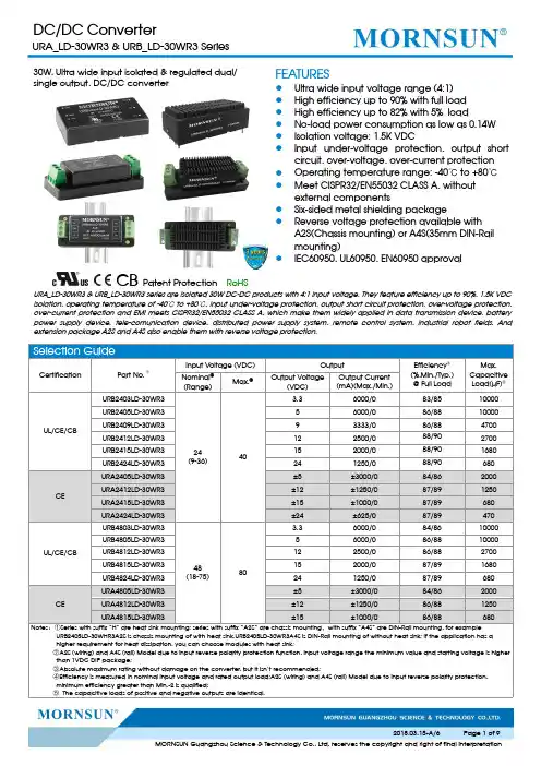
30W,Ultra wide input isolated ®ulated dual/single output,DC/DC converterCB Patent ProtectionRoHSFEATURES●Ultra wide input voltage range (4:1)●High efficiency up to 90%with full load ●High efficiency up to 82%with 5%load●No-load power consumption as low as 0.14W ●Isolation voltage:1.5K VDC●Input under-voltage protection,output short circuit,over-voltage,over-current protection ●Operating temperature range:-40℃to +80℃●Meet CISPR32/EN55032CLASS A,without external components●Six-sided metal shielding package●Reverse voltage protection available with A2S(Chassis mounting)or A4S(35mm DIN-Rail mounting)●IEC60950,UL60950,EN60950approvalURA_LD-30WR3&URB_LD-30WR3series are isolated 30W DC-DC products with 4:1input voltage.They feature efficiency up to 90%,1.5K VDC isolation,operating temperature of -40℃to +80℃,Input under-voltage protection,output short circuit protection,over-voltage protection,over-current protection and EMI meets CISPR32/EN55032CLASS A,which make them widely applied in data transmission device,battery power supply device,tele-comunication device,distributed power supply system,remote control system,industrial robot fields.And extension package A2S and A4S also enable them with reverse voltage protection.Product Characteristic CurveFig.1Apply model :URA2405LD-30W(H)R3(9-18V input voltage )、URA2424LD-30W(H)R3(9-18V input voltage )、URA4805LD-30W(H)R3(18-36V input voltage )Fig.2Apply model :URA2405LD-30W(H)R3(18-36V input voltage )、URA2424LD-30W(H)R3(18-36V input voltage )、URA4805LD-30W(H)R3(36-75V input voltage )、URA2412LD-30W(H)R3、URA2415LD-30W(H)R3、URA4812LD-30W(H)R3、URA4815LD-30W(H)R3Fig.3Apply model :URB2403LD-30W(H)R3、URB2405LD-30W(H)R3、URB4803LD-30W(H)R3、URB4805LD-30W(H)R3Fig.4Apply model :URB2409LD-30W(H)R3、URB2412LD-30W(H)R3、URB2415LD-30W(H)R3、URB2424LD-30W(H)R3、URB4812LD-30W(H)R3、URB4815LD-30W(H)R3、URB4824LD-30W(H)R3All the DC/DC converters of this series are tested according to the recommended circuit(see Fig.5)before delivery.If it is required to further reduce input and output ripple,properly increase the input&output of additional capacitors Cin and Cout or select capacitors of low equivalent impedance provided that the capacitance is no larger than the max.capacitive load of the product.V in0VV in0VDual outp ut:Single outputvoltage(VDC)Cout(µF)Cin(µF)Dual outputvoltage(VDC)Cout(µF)Cin(µF)3.3/5/9220100±5/±12/±1522010012/15/24100±241002.EMC solution-recommended circuitSingle outputFig.6Notes:Part①in the Fig.6is used for EMC test and part②for EMI filtering;selected based on needs.Parameter descriptionModel Vin:24V Vin:48VFUSEChoose according to actual inputcurrentMOV S20K30S14K60C0680µF/50V330µF/100VC1330µF/50V330µF/100VC2 4.7µF/50V 2.2µF/100VC3Refer to the Cout in Fig.5LCM1mH,recommended to useMORNSUN’s FL2D-30-102sCY1、CY21nF/2KVDual outputFig.7Notes:Part①in the Fig.7is used for EMC test and part②for EMI filtering;selected based on needs.Model Vin:24V Vin:48VFUSE Choose according to actual inputcurrentMOV S20K30S14K60C0680µF/50V330µF/100VC1 2.2µF/50V 2.2µF/100VC2 2.2µF/50V 2.2µF/100VC3330µF/50V330µF/100VC4Refer to the Cout in Fig.5LDM1 3.3µHCY1、CY2 2.2nF/400V AC Safety Y Capacitor3.Application of Trim and calculation of Trim resistanceTrim up Trim downApplied circuits of Trim(Part in broken line is the interior of models)Calculation formula of Trim resistance:up: a=VrefVo’-VrefR1R=TaR2R-a2-R3down: a=VrefVo’-VrefR2R=TaR1R-a1-R3R T is Trim resistance,a is a self-definedparameter,with no real meaning.Vo’for the actual needs of the up ordown regulated voltageVout(VDC)R1(KΩ)R2(KΩ)R3(KΩ)Vref(V)3.34.801 2.8712.4 1.245 2.883 2.8710 2.597.500 2.8715 2.51211.000 2.8715 2.51514.494 2.8715 2.52424.872 2.8717.8 2.54.It is not allowed to connect modules output in parallel to enlarge the power5.For more information please find DC-DC converter application notes on Horizontal Package(without heat sink)Dimensions and Recommended LayoutHorizontal Package(with heat sink)DimensionsURA_LD-30WR3A2S&URB_LD-30WR3A2S(without heat sink)DimensionsNotes:1.Packing information please refer to Product Packing Information which can be downloaded from .Horizontal Packing Bag Number:58200035(without heat sink),58200051(with heat sink),A2S/A4S Packing Bag Number:58220022;2.The maximum capacitive load offered were tested at input voltage range and full load;3.Unless otherwise specified,parameters in this datasheet were measured under the conditions of Ta=25℃,humidity<75%RH with nominalinput voltage and rated output load;4.All index testing methods in this datasheet are based on Company’s corporate standards;5.We can provide product customization service,please contact our technicians directly for specific information;6.Products are related to laws and regulations:see"Features"and"EMC";7.Our products shall be classified according to ISO14001and related environmental laws and regulations,and shall be handled byqualified units.Mornsun Guangzhou Science&Technology Co.,Ltd.Address:No.5,Kehui St.1,Kehui Development Center,Science Ave.,Guangzhou Science City,Luogang District,Guangzhou,P.R.China Tel:86-20-38601850-8801Fax:86-20-38601272E-mail:***************。
DC-DC 电源转换器基本原理

DC-DC 电源转换器基本原理,Mar. 26th, 2012目录DCDC DC--DC 转换器简介交换式电源结构框图交换式电源原理介绍交换式电源设计实例 交换式电源交换式电源线路重要参数线路重要参数DC-DCDC DC 转换器简介电源对于电设备犹如心脏对于人体,是所有电设备的动力。
早期,电设备功能单一,基本上直接用变压器将交流市电转换为所需的直流电压即可满足要求。
但随着电子设备功能日益多样,其系统线路也越来越复杂,对电源的要求也越来越高。
同时,以轻便、小巧为发展趋势的电子产品,不可能允许每组power都由体积大、干扰强的交流变压器来实现。
因此,研发都由体积大干扰强的交流变压器来实现因此研发直流到直流的电源转换成为必须。
把直流电压变换为另一种直流电压最简单的办法是串电阻,把直流电压变换为另种直流电压最简单的办法是串电阻但是由于焦耳热的消耗,会使这种方式转换的效率非常低,它只适用于电流极小的电压转换另外利用半导体器件只适用于电流极小的电压转换。
另外,利用半导体器件(如PN结)的电压drop能力实现降压,也就是所谓的LDO 方式,这种方式DC-DC 的损耗比直接用电阻会好很多,但依然存在效率低、过电流能DC DC 转换器简介力有限、电压drop 范围小等局限性。
变换Figure-1传统式DC-DC 变换器在计算机出现之后,由于其对大loading power oad g po e 的需求,使得传统的DC-DC 变换器已完全不可能再满足设计需求。
思考:请充分发挥想象,思考实现电压变换还有什么方法?提示排列组合能引发质变能产生奇迹提示:排列组合能引发质变,能产生奇迹。
DC-DC 在power 转换中,由于电感、电容对脉动电流和电压的滞后DC DC 转换器简介p 转换中容对动滞后性以及其对能量的储存性,再配合以精准的反馈回路,可以实现电压转换功能.Figure 2DC DC Figure-2交换式DC-DC 变换器交换式电源原理介绍基本交换式电源转换器电路(Buck转换器)Figure-4基本交换式电源转换器电路(Buck转换器)交换式电源原理介绍Figure-5基本交换式电源转换器电路(Buck转换器)交换式电源原理介绍稳态分析(CCM)a. Q1导通时)V V VV L(t)=V L(ON)=V I-V O)=(0)+(V)/Li L(t)i L(0)+( V L(t)dt)/L=i L(0)+(V I-V O)t/L则t = t(ON) = DT S时, 由上式可得知: )(0)(V V/L D: Duty Cyclei L(DT S)=i L(0)+(V I-V O)DT S/L 1基本交换式电源转换器电路(Buck转换器)交换式电源原理介绍Figure-6交换式电源原理介绍基本交换式电源转换器电路(Buck转换器)稳态分析(CCM)b. Q1截止时V L(t)V L(OFF)V O)=-V=-Vi L(t)=i L(DT S)+( V L(t)dt)/L=i L(DT S)+(-V O)(t-DT S)/Lt T时由上式可得知则t = T S 时, 由上式可得知:i L(T S)=i L(DT S)+(V O)(1D)T S/L 2)+(-V1-D)T/L基本交换式电源转换器电路(Buck转换器)交换式电源原理介绍稳态分析(CCM)c. 当转换器在稳态时i L T S )= i L (0)()()由1, 2 兩式可得出21因此:i L (T S )=i L (0)+(V I -V O )DT S /L+(-V O )(1-D)T S /L(V I -V O )DT S = V O (1-D)T S或者:V L(ON)DT S = V L(OFF)(1-D)T SV O /V I = D = t ON /T S基本交换式电源转换器电路(Boost转换器)交换式电源原理介绍Figure-7基本交换式电源转换器电路(Boost转换器)交换式电源原理介绍稳态分析(CCM)a. Q1导通时V L )=V I (t )i L (t )=i L (0)+( V L (t )dt )/L=i L (0)+V I t /Lt =(ON)=DT 时由上式可得知:D:Duty Cycle 则t = t (ON) = DT S 时, 由上式可得知:)=/LD: Duty Cycle i L (DT S )i L (0)+V I DT S /L 3基本交换式电源转换器电路(Boost转换器)交换式电源原理介绍2.2 升压型(boost)转换器Figure-8交换式电源原理介绍基本交换式电源转换器电路(Boost转换器)稳态分析(CCM)b. Q1截止时V L(t) = -(V O-V I))(V Vi L(t)=i L(DT S)+( V L(t)dt)/L=i L(DT S)+[-(V O-V I)](t-DT S)/L则t = T S 时, 由上式可得知:i L(T S)=i L(DT S)+[-(V O-V I)(1-D)T S/L 4))+[(V V1D)T/L基本交换式电源转换器电路(Boost转换器)交换式电源原理介绍Figure-9基本交换式电源转换器电路(Boost转换器)交换式电源原理介绍稳态分析(CCM)c. 当转换器在稳态时)=i L (T S ) i L (0)由1, 2 兩式可得出43因此:i L (T S )=i L (0)+V I DT S /L+[-(V O -V I )](1-D)T S /LV I DT S = (V O -V I )(1-D)T S或者或者:V O /V I =1/(1-D)交换式电源设计实例交换式电源实例讲解以Buck线路为例,其拓扑形式在实际的应用中很少用续流二极管,因为续流二极管的反向电流很大,损耗太严重。
buck电路的阻抗变换
buck电路的阻抗变换Buck电路是一种常见的降压转换器,广泛应用于电源管理系统中。
在设计和分析Buck电路时,了解阻抗变换对电路性能的影响是非常重要的。
本文将介绍Buck电路的阻抗变换以及如何应用这些变换来分析电路。
1. Buck电路简介Buck电路是一种DC-DC转换器,用于将高输入电压转换为较低的输出电压。
它由功率开关、电感和输出电容组成。
根据电感和开关的工作状态,Buck电路可以实现电流连续和不连续两种模式。
2. 阻抗变换原理阻抗变换是指通过改变电路元件的参数来改变电路的输入输出特性。
在Buck电路中,常用的阻抗变换方法有:2.1 变换电感值:通过改变电感的数值,可以调节电路的谐振频率和输出电压范围。
2.2 变换负载电阻:改变负载电阻的数值可以调节电路的输出电压和电流。
2.3 变换开关频率:通过改变开关频率,可以调节电路的效率和输出电压波动。
3. 阻抗变换在Buck电路中的应用3.1 变换电感值:当需要调节Buck电路的输出电压时,可以通过改变电感的数值来实现。
增大电感值可以降低输出电压,减小电感值则可以提高输出电压。
3.2 变换负载电阻:负载电阻对Buck电路的输出电压和电流有较大影响。
通过改变负载电阻的数值,可以调节输出电压和电流到所需的数值。
3.3 变换开关频率:开关频率决定了Buck电路的工作速度和效率。
较高的开关频率可以提高电路的响应速度和效率,但也可能增加开关损耗。
通过调节开关频率,可以在输出电压和效率之间找到合适的平衡点。
4. 阻抗变换的分析方法在分析Buck电路中的阻抗变换时,一种常用的方法是采用频域分析。
通过将电路转换为复数形式,可以用相量和极坐标的形式来表示电路元件的阻抗。
在频域中,可以通过计算阻抗间的复数运算来得到电路的传输函数和频率响应。
5. 案例研究:变换电感值对Buck电路的影响以一个常见的Buck电路为例,假设电感的数值从L1变为L2,其他参数保持不变。
通过频域分析,可以计算出电路的新传输函数和频率响应。
dcdc转换器原理
dcdc转换器原理DC-DC转换器是一种将一种直流电压转换成另一种直流电压的电子装置。
它通常由一个开关电路和一个储能电感组成,可以将高电压的直流电转化为低电压的直流电,也可以将低电压的直流电转化为高电压的直流电,具有普遍的应用。
下面,我们将从DC-DC转换器的原理出发来讲述它的工作原理和具体的实现过程。
1. PWM控制DC-DC转换器是通过PWM控制来实现的。
PWM控制是指记录一个给定周期内的占空比,然后依据这个占空比来控制输出电压的平均值。
2. 基本电路DC-DC转换器基本电路图由开关、储能电感、输出滤波电容等器件组成。
而在使用中,开关也就成了MOS管。
3. 工作方式DC-DC转换器根据开关的切换频率,分为脉冲模式和连续模式。
a. 脉冲模式在脉冲模式下,当MOS管开启时,电感中的电流逐渐增加,储能到电感中。
当MOS管关闭时,这个电流将绕过回路,去激励输出负载。
b. 连续模式当MOS管开启时间足够长时,电流是连续的。
如果调整开启时间短,就达到了脉冲模式。
在连续模式下,开关频率越高,输出电压的纹波越小。
4. 输出电压输出电压的大小,与开关时的时间和一定电感与负载的比例有关。
我们可以通过精确定义PWM信号来控制输出电压的稳定性。
5. 应用DC-DC转换器是用来处理不同电压方案的一种有效方法。
在很多应用中,例如车载电子、手机、笔记本,都有DC-DC转换器的应用。
总之,DC-DC转换器通过控制开关来实现电压升降的目的,直接作用对象是输入和输出电压,为其他电器和代替传统的线性稳压技术提供了先进的电源解决方案。
DCDC转换器
DC/DC转换器
简阳市高级职业中学 朱宝全
案例引入
某北汽 4S 店的高级汽车维修工小王接到一张任务工作单:车主在对一辆北汽 EV160纯电动汽车自行清洗时,因操作不当,导致洗完后出现车辆仪表充电指示灯 点亮、车辆无法行驶的故障。
2
思考:需要检查哪些设备?
3
复习
4
回答
5
学习任务
2.测量熔断器及 连接线束通断。
1.测量低压 蓄电池电压。
14
4.测量高压控 制盒内对应熔 断器的通断。
四、 DC/DC转换器的检测
1、测量低压蓄电池电压
保证整车线 束正常连接的情 况下,上电前用 万用表测量铅酸 蓄电池电压,并 记录;测量得知 蓄电池电压为 12.5v,结果正常。
15
四、 DC/DC转换器的检测
11
三、 DC/DC转换器的工作条件及工作原理
2、DC/DC转换器的工作过程
当VCU控制IGBT2和 IGBT3导通时,动力电池 组件电流从正极流经 IGBT2至变压器初级绕组 上端,向下流过初级绕组, 经IGBT3到动力电池组件 负极,完成回路。
12
三、 DC/DC转换器的工作条件及工作原理
2、DC/DC转换器的工作过程
7
二、DC/DC转换器的电路连接及端口
1、DC/DC转换器电路连接图
8
二、DC/DC转换器的电路连接及端口
2、DC/DC端口定义
低压输 出正极
低压输 出负极
BA CA B
高压输入端
A脚:电源负极
B脚:电源正极
9 中间为高压互锁短接端子
低压控制端 A脚:控制电路电源正兼使能(直流12V启动,0~1V关机) B脚:电源状态信号输出(故障线,故障:12V高电平,正 常:低电平) C脚:控制电路电源负
新能源汽车dcdc转换器工作原理
新能源汽车dcdc转换器工作原理
新能源汽车DC-DC转换器是一种特殊的电源转换器,用于将高电压直流电能(例如高压锂电池组输出的400V DC)转换为低电压直流电能(例如12V DC)。
这种转换器的工作原理基于电磁感应和电子元件控制技术。
在工作过程中,首先将高压直流电接入DC-DC转换器的输入端,然后通过变换器电路开始进行电源转换。
变换器电路由几个功率半导体器件组成,例如MOSFET和二极管。
通过对这些器件的控制和调节,可以将输入的高电压直流电能通过电感等元件变换为特定电压和电流的低电压直流电能输出。
在DC-DC转换器中,还有一个重要的控制单元,即PWM控制单元。
这个单元起到了监控和控制功率半导体器件的作用。
PWM控制单元以不同的占空比控制器件的导通和截止,从而控制输出电流和电压的稳定性和准确性。
综合来看,新能源汽车DC-DC转换器的工作原理建立在先进的电子元件控制和电磁感应技术之上。
它能够将高压直流电能转换为低电压直流电能,并确保输出电流和电压的稳定性和准确性。
这种转换器在新能源汽车的电力系统中具有非常重要的作用。