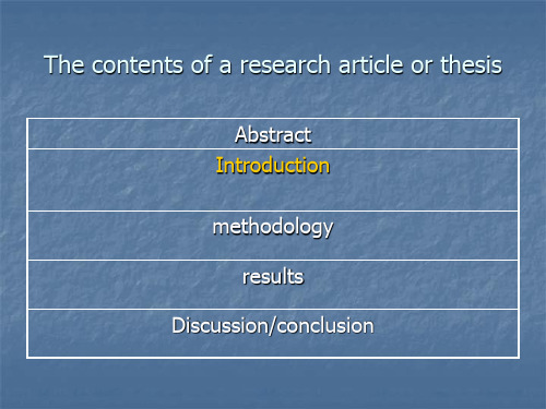
1. Introduction
英语写作第一节课introduction

18
Comparing some terms
―subject‖, ―topic‖ and ―title‖
19
―subject‖, ―topic‖ and ―title‖
• Subject: is the thing, person, idea or event that is being discussed, written about, or considered. e.g. the subject of a discussion, letter, book • Topic: The topic is a particular subject that is written about or discussed. • Title: The title of a book, play, piece of music is the name given to it by the person who wrote it or composed it, or the name by which it is usually known.
Choose which are subjects and topics? sports, foreign students in U.S Universities, what makes a champion soccer player, education, why I play soccer, my first trip abroad, open classrooms and traditional classrooms, one tour in the USA, world travel, music in elementary school
It moves down and up conforming to the Writing task Meanwhile, her double chin is her rhythm. another great feature, which seems to give her voice more power. Above all, you can see what an extraordinary woman she is, so can you guess who she is?
英语论文分析学习 第1节 introduction
What Is an Introduction?
What questions will readers ask when reading an essay: 1. What topic am I going to learn about? 2. Why is that topic important? 3. Do I know the topic already? What do I know already? An introduction aims to answer these 3 questions.
Contents of an introduction
Example:
"Numerous studies on the utilization of plant proteins as a partial or complete replacement for fish meal in diets have been conducted using various freshwater and marines fishes (Lovell, 1987; Tacon et al., 1983; Murai et al., 1989a; Cowey et al., 1974).
Contents of an introduction
Q: What are the ways to establish a topic? A: Claiming centrality General to specific Previous research Describing of the background Definition of key words
[英语学习]unit-1-Introduction
![[英语学习]unit-1-Introduction](https://img.taocdn.com/s3/m/c54459bff7ec4afe05a1df71.png)
展。
• a Panorama of Publishing 出版业概况 • book industry 图书出版业 • book community 书业团体
Questions on part 1
• 1 [+ obj] : to prepare and produce (a book, magazine, etc.) for sale ▪ It's a small company that only publishes about four books a year. ▪ The university press publishes academic titles. ▪ The newspaper is published daily. 2 : to have something you wrote included in a book, magazine, newspaper, etc. [no obj] ▪ There is a lot of pressure for professors to publish regularly. [+ obj] ▪ He has not published anything for a long time. 3 [+ obj] : to include (an article, letter, photograph, etc.) in a magazine or newspaper ▪ The magazine published two of my stories.
3. intriguing
introduction 造句
introduction 造句introduction 造句:1.He made theself-introduction and everyone shook hands with him.他作了自我介绍,大家都与他握了手。
2.Please be aware that this is only a selection of essential requirements ofthe organic standards, meant as an introduction.请注意,这只是一个有机标准必需要求的精选摘要,仅作介绍。
3.The article givessort of a general introduction concerning the back story of the game, and the general feel .文章整体介绍了游戏故事背景和对其的印象。
4.Therefore,the enemy would like to ask all the detailed re-usedan introduction.所以想问问都用过的冤家详细的再引荐下。
5.About this trip here first simple introduction, the specific content, everybody can consult brochure or visit our websit e to understand.关于这次旅程就先简单介绍到这里,具体的内容,大家可以参照小册子或是登陆我们的网站进行了解。
6.I also wonder if it is possible for research articles to be produced by a historical and popular introduction.我想,是否有可能通过历史的、通俗的介绍来撰写研究论文。
unit_1_introduction[1]
![unit_1_introduction[1]](https://img.taocdn.com/s3/m/5a44843a10661ed9ad51f372.png)
1.1 Text(2)
• According to the information direction transmitted in channel, modern communication systems can be divided into the simplex communication systems, half-duplex communication systems, and full-duplex communication systems; • According to the number of information communicating approaches, modern communication systems can be divided into the serial communication systems and the parallel communication systems; • According to the control methods of information transmitted in channels, modern communication systems can be divided into the synchronous communication systems and the asynchronous communication systems; • According to the line connecting modes and signal interacting ways between signal source and destination, modern systems can be divided into point-to-point communication systems, one-to-multi-points communication systems and multi-to-multi-points communication systems.
1 INTRODUCTION 传感与检测技术
1 INTRODUCTION TO SENSORBASED MEASUREMENT SYSTEM
1.1 GENERAL CONCEPTS AND TERMINOLOGY 1.1.1 Measurement Systems System: a combination of two or more elements, subsystems, and parts necessary to carry out one or more functions. The function of a measurement system: the objective and empirical assignment of a number to a property or quality of an object or event in order to describe it.
The best approach is to design systems insensitive to interference.
1.3 GENERAL INPUT-OUTPUT CONFIGRATION
Common method: . negative feedback.
y ( x yH ( s ))G ( s ) Y ( s) G ( s) 1 X (s) 1 G (s) H (s) H x
1.3 GENERAL INPUT-OUTPUT CONFIGRATION
1.3.2 Compensation Techniques Reduce the effects of interfering and modifying inputs:
• Change the system design • Add new elements to it
1.Introduction+structures
I. Classification of Writings
A. Literature Writings B. Scientific Writings (factual writings)
II. Principles for Good Scientific Writing (1)
Content: original Organization/Structure: complete, coherent Language: correct 文风有独创性;主题 处理好; 中心思想明确; 行文逻辑严密;选辞精确;句子、段落表达 完整;阅读效果好;没有错别字及语法、标 点符号的错误。
Brief & Simple
Though I usually go to the country for a walk during the weekend, I decided to spend the whole day in the city for a change last Sunday. I went to the Tian’anmen Square and the Zhongshan Park. It was so early when I left home that the streets around my neighborhood were deserted. Without the usual crowds and traffic, everything was strangely quiet.
Writing Suggestions:
Plan your writing (audience awareness / target readers). Ignore the language. Write and rewrite. Find readers. Keep writing. Find suitable methods from handbooks and guides. There is many a way to write.
情景英语1(introduction)
Scene 1: You are the new comer to the office. You meet your new coworker Peter Smith in the office. Please introduce each other and have a very nice greeting.
A: David! It’s great to see you! you look as young as ever And you must B: Philip, ___________________________. be Roger. C: Hi. A: Yes, this is my youngest son Roger. Roger, I want you to meet the king dancer of tango of Harvard— David Lin. C: Nice to meet you, Mr. Lin. B: Well, you are so tall. How old are you this year? C: Seven. we haven’t seen each other for years since our graduation, B: So ______________________________________________, Philip. Well, how’ve you been? A: Oh, working too hard.
A: Good evening, Mr. Wu. B: Good evening, Mr. Smith. A: Have you met my wife, Juliet? I haven’t had the pleasure B: No,______________________________. A: Mary, this is Mr. Wu, my Chinese friend. C: How do you do, Mr. Wu? Welcome. B: How do you do? Have a glass of wine Mr. Wu. A:_____________________, let me introduce you to some of my guests. And___________________________________________. B: Thank you.
1.introduction 简介
Introduction
1、生物化学的概念 2、生物化学的发展简史
3、生物化学的主要研究内容 4、生物化学与其它学科的关系
生物化学的概念
生物化学是研究生命 化学的学科,它在分子水 平上探讨生命的本质,即 研究生物体的分子结构与 功能,物质代谢与调节, 及其在生命活动中的作用。
①吴宪
在血液化学分析方面创 立了血滤液的制备和血糖测定法; ②蛋白质方面,提出了蛋白质变 性学说; ③免疫学方面,研究抗原抗体的 反应机制;
④1965年,首先人工合成具
有生物活性的胰岛素; ⑤1981年,成功合成酵母丙 氨酰tRNA; ⑥完成人类基因组计划工作 的1%。
生物化学的研究内容
静态生物化学 动态生物化学 1、 功能生物化学 分子生物学 2、生物化学的研究采用化 学的原理和方法; 3、生物化学与细胞学、遗传学、 生理学关系密切;
生物化学的发展简史
1、初级阶段
2、发展阶段 3、分子生物学阶段
4、现状
初级阶段
1、对糖类、脂类、氨基酸作
了比较系统的研究; 2、发现了核酸; 3、化学合成了简单多肽; 4、酵母发酵过程中可溶性催 化剂的发现奠定了酶学的基础。
1、生物大分子的结构与功能; 2、物质代谢及其调节; 3、基因信息的传递及其调控。
生物大分子:由某些 基本结构单位按照一定的 顺序和方式连接所形成的 多聚体。 分子量一般在104以上
生物化学与其他学科的关系
1、与农业的关系 2、与工业的关系 3、与药学的关系 4、与医学的关系
与农业的关系
人类基因组计划
科学研究证明,人类的生老病死
都与基因有关,如果能够破译人 类基因的序列和功能,就有可能 真正有效地预防、诊断和治疗各 种疾病。因此,1990年正式启动 的人类基因组计划一开始就引起 了全世界的广泛关注。
1. INTRODUCTION
1. INTRODUCTION1.1. WHY USE ELECTRONS?Why should we use an electron microscope? Historically, TEMs were developed because of the limited image resolution in light microscopes, which is imposed by the wavelength of visible light. Only after electron microscopes were developed was it realized that there are many other equally sound reasons for using electrons, most of which are utilized to some extent in a modern TEM. By way of introduction to the topic let's look at how the TEM developed and the pros and cons of using such an instrument.1.1.A. An Extremely Brief HistoryLouis de Broglie (1925) first theorized that the electron had wave-like characteristics, with a wavelength substantially less than visible light. Then Davisson and Germer (1927) and Thompson and Reid (1927) independently carried out their classic electron diffraction experiments which demonstrated the wave nature of electrons. It didn't take long for the idea of an electron microscope to be proposed, and the term was first used in the paper of Knoll and Ruska (1932). In this paper they developed the idea of electron lenses into a practical reality, and demonstrated electron images taken on the instrument shown in Figure 1.1. This was a most crucial step, for which Ruska received the Nobel Prize, somewhat late, in 1986. Within a year of Knoll and Ruska's publication, the resolution limit of the light microscope was surpassed. Ruska, surprisingly, revealed that he hadn't heard of de Broglie's ideas about electron waves and thought that the wavelength limit didn't apply to electrons. TEMs were developed by commercial companies only four years later. The Metropolitan-Vickers EM 1 was the first commercial TEM. It was built in the UK in 1936, but apparently it didn't work very well and regular production was really started by Siemens and Halske in Germany in 1939. TEMs became widely available from several other sources (Hitachi, JEOL, Philips and RCA, inter alia) after the conclusion of World War II.For materials scientists a most important development took place in the late 1940s when Heidenreich (1949) first thinned metal foils to electron transparency. This work was followed up by Bollman in Switzerland and Hirsch and co-workers in Cambridge. Because so much of the early TEM work examined metal specimens, the word "foil" has come to be synonymous with "specimen." In addition, the Cambridge group also developed the theory of electron diffraction contrast with which we can now identify, often in a quantitative manner, all known line and planar crystal defects in TEM images. This theoretical work is summarized in a formidable but essential text often referred to as the "Bible" of TEM (Hirsch et al. 1977). For the materials scientist,practical applications of the TEM for the solution of materials problems were pioneered in the United States by Thomas and first clearly expounded in his text (Thomas 1962). Other materials-oriented texts followed, e.g., Edington (1976) and Thomas and Goringe (1979).Today, TEMs constitute arguably the most efficient and versatile tools for the characterization of materials. If you want to read a history of the TEM, the book by Marton (1968) is a compact, personal monograph and that edited by Hawkes (1985) contains a series of individual reminiscences. Fujita (1986) emphasizes the contribution of Japan to the development of the instrument. The field is now at the point where many of the pioneers have put their memoirs down on paper, or Festschrifts have been organized in their honor (e.g., Cosslett 1979, Ruska 1980, and Hashimoto 1986) which detail their contributions over the decades, and compile some useful overview papers of the field. If you enjoy reading about the history of science, we strongly recommend the review of Fifty Years of Electron Diffraction, edited by Goodman (1981), and Fifty Years of X-ray Diffraction, edited by Ewald (1962). (The spelling of X-ray is discussed in the CBE Manual, 1994.)Figure 1.1. The electron microscope built by Ruska and Knoll in Berlin in the early 1930s.1.1.B. Microscopy and the Concept of ResolutionWhen asked what a "microscope" is, most people would answer that it is an instrument for magnifying things too small to see with the naked eye, and most likely they would be referring to the visible-light microscope. Because of the general familiarity with the concept of the light microscope, we will draw analogies between electron and visible-light microscopes wherever it's instructive.The smallest distance between two points that we can resolve with our eyes is about 0.1-0.2 mm, depending on how good our eyes are, and assuming that there's sufficient illumination to see by. This distance is the resolution or resolving power of our eyes. So any instrument that can show us pictures (or "images" as we'll refer to them) revealing detail finer than 0.1 mm could be described as a microscope, and its highest useful magnification is governed by its resolution. A major attraction to the early developers of the TEM was that, since electrons are smaller than atoms, it would be possible, at least theoretically, to build a microscope that could "see" detail well below the atomic level. The idea of being able to "see" with electrons may be confusing to you. Our eyes are not sensitive to electrons. If a beam of high-energy electrons was aimed into your eye, you would most likely be blinded as the electrons killed the retinal cells, but you wouldn't see anything! So an integral part of any electron microscope is a viewing screen of some form, which translates electron intensity to light intensity, and which we observe or record photographically. We'll discuss these screens and other ways of recording electron images in later chapter.The resolution of a TEM means different things for different functions of the instrument, and we'll discuss them in the appropriate chapters. It's easiest to think of the image resolution in TEM in terms of the classical Rayleigh criterion for light microscopy, which states that the smallest distance that can be resolved, , is given approximately by δβµλ=δsin 61.0 [1.1]In equation 1.1, is the wavelength of the radiation, is the refractive index of the viewing medium, and is the semiangle of collection of the magnifying lens. For the sake of simplicity we can approximate sin (which is sometimes called the numerical aperture) to unity and so the resolution is equal to about half the wavelength of light. For green light in the middle of the visible spectrum, is about 550 nm (5500Å), and so the resolution of a good light microscope is about 300 nm. In TEMs we can approximate the resolution in equation 1.1 to 0.61/ which, as we'll see later, is very small.λµβµβλλβNow although 300 nm is a small dimension to us it corresponds to about 1000 atom diameters, and therefore many of the features that control the properties of materials are on a scale well below the resolution of the light microscope. So there's a real need to image detail down to the atomic level if we want to understand the properties of materials, and that's a major reason why TEMs are so useful.We'll try to use nanometers throughout this book, but you'll find that many microscopists still insist on using Angstroms rather than the SI units. However, the Angstrom is close to the atomic diameter and so is a more convenient unit because it saves us using convoluted phrases like “three tenths of a nanometer.”This limit of light microscopy was well understood at the turn of this century and prompted Ernst Abbe, one of the giants in the field, to complain that "it is poor comfort to hope that human ingenuity will find ways and means of overcoming this limit." (He was right to be so depressed because he died in 1905, some 20 years before de Broglie's ingenuity solved the problem.) Now de Broglie's famous equation shows that the wavelength of electrons is related to their energy, E, and if we ignore relativistic effects we can show approximately (and exactly in Section 1.4 below) that2/122.1~Eλ [1.2]In this equation E is in electron volts (eV) and in nm. Remember that we should be precise in our use of the units V and eV: the former represents the accelerating voltage of the microscope while the latter refers to the energy of the electrons in the microscope. So for a 100-keV electron, we find that ~ 4 pm (0.004 nm), which is much smaller than the diameter of an atom.λλFigure 1.2. A twin boundary in spinel stepping from one {111} plane to another parallel plane. The white dots are columns of atoms. The change in atomic orientation across the twin boundary can be readily seen, even if we do not know what causes the white dots or why, indeed, they are white.We'll see later that we are nowhere near building TEMs that approach this wavelength limit of resolution, because we can't make perfect electron lenses (see Section 2). But progress was rapid after Ruska's early work on lenses and, since the mid-1970s, many commercial TEMs have been capable of resolving individual columns of atoms in crystals, creating the field of "high-resolution transmission electron microscopy," or HRTEM. A typical HRTEM image is shown in Figure 1.2. The advantages of shorter wavelengths led in the 1960s to the development of high voltage electron microscopes (HVEMs), with accelerating potentials between 1 MV and 3 MV . In fact, most of these instruments were used to introduce controlled amounts of radiation damage into specimens in an attempt to simulate nuclear reactor environments, but changes in the emphasis of energy research mean there is not much call for such instruments today. While we can still improve the resolution byincremental amounts, the drive for much better resolution is now no longer paramount and the TEM is developing in other ways. In fact, only one HVEM (1 MV) for HRTEM imaging was constructed in the 1980s and three 1.25-MV machines in the 1990s. Intermediate voltage electron microscopes (IVEMs) were introduced in the 1980s. These TEMs operate at 300 or 400 kV, but still offer very high resolution, close to that achieved at 1 MV.1.1.C. Interaction of Electrons with MatterElectrons are one type of "ionizing radiation," which is the general term given to radiation that is capable of removing one of the tightly bound inner-shell electrons from the attractive field of the nucleus.One of the advantages to using ionizing radiation is that it produces a wide range of secondary signals from the specimen, and some of these are summarized in Figure 1.3. Many of these signals are used in "analytical electron microscopy,'' or AEM, giving us chemical information and a lot of other detail about our samples. AEM uses X-ray energy dispersive spectrometry (XEDS) and electron energy-loss spectrometry (EELS). For example, Figure 1.4A is an X-ray spectrum from a very small region of a TEM specimen showing characteristic peaks which identify the elements present. We can transform such spectra into quantitative data describing elemental changes associated with inhomogeneous microstructures as also shown in Figures 1.4B and C. In contrast, microscopes using nonionizing radiation such as visible light usually only generate light (but not much heat, which is good). AEMs generally offer improved performance at intermediate voltages, similar to HRTEMs.Figure 1.3. Signals generated when a high-energy beam of electrons interacts with a thin specimen. Most of these signals can be detected in different types of TEM. The directions shown for each signal do not always represent the physical direction of the signal but indicate, in a relative manner, where the signal is strongest or where it is detected.In order to get the best signal out of our specimens we have to put the best signal in, and so the electron source is critical. We are now very accomplished in this respect as you'll see in Section 4, so modern TEMs are very good signal-generating instruments. To localize these signals we need to get our TEM to form a very fine electron beam, typically <10 nm and at best <1 nm in diameter. We accomplish this by combining TEM and scanning electron microscope (SEM) technology to create a scanning transmission electron microscope (STEM). The STEM is both the basis for AEMs and a unique scanning imaging microscope in its own right. In fact there are instruments that are only capable of operating in scanning mode and these are sometimes referred to as "dedicated STEMs," or DSTEMs.1.1.D. Depth of FieldThe depth of field of a microscope is a measure of how much of the object we are looking at remains "in focus" at the same time. Like the resolution, this property is governed by the lenses in the microscope. The best electron lens is not a very good one, as we've already mentioned, and has been compared to using the bottom of a Coca-Cola bottle as a lens for light microscopy. To minimize this problem we have to use very small limiting apertures in the lenses, narrowing the beam down to a thin "pencil" of electrons which at most is a few micrometers across. These apertures cut down the intensity of the electron beam, but also act to increase the depth of focus of the images that we produce. Remember that "depth of field" refers to the specimen while "depth of focus" refers to the image.While this large depth of field is chiefly used in the SEM to produce 3D-like images of the surfaces of specimens with large changes in topography, it is also critical in the TEM. It turns out that in the TEM, all of the specimen is usually in focus at the same time, independent of the specimen topography, as long as it's electron transparent! Figure 1.5 shows a TEM image of some dislocations in a crystal. The dislocations appear to start and finish in the specimen, but in fact they are threading their way through the specimen from the top to the bottom, and they remain in sharp focus at all times. Furthermore, we can record the final image at different positions below the final lens of the instrument and it will still be in focus. Compare this with the visible-light microscope where, as you probably know, unless the surface of the specimen is flat to within the wavelength of light, it is not all in focus at the same time. This aspect of TEM gives us both advantages and disadvantages in comparison to the visible-light microscope.A BC Figure 1.4. (A) An X-ray spectrum from asmall biotite crystal showing peaks atenergies that are characteristic of theelements present in the region thatinteracts with the electron beam. Themajor peaks from left to right are for Mg,Al, Si, K, Fe, and the Cu support grid. (B)A TEM image of a precipitate-free zone(PFZ) in an aged Al-16 wt% Ag alloy. (C)The Ag profile across the PFZ in (B),obtained through X-ray spectrometry inthe TEM showing the depletion of Agresponsible for the PFZ formation.Figure 1.5. TEM image of dislocations in GaAs. A band of dislocations threads through the thin specimen from the top to the bottom but remains in focus through the foil thickness.1.1.E. DiffractionThompson and Reid showed that electrons could be diffracted when passing through thin crystals of nickel, and the possibility of combining electron diffraction into TEMs was realized by Kossel and Mollenstedt (1939). Today, electron diffraction is an indispensable part of TEM and is arguably the most useful aspect of TEM for materials scientists. Figure 1.6 shows a TEM diffraction pattern which contains information on the crystal structure, lattice repeat distance, and specimen shape, as well as being a most striking pattern. We'll see that the pattern can always be related to the image of the area of the specimen from which it came, in this case shown in the inset. In addition to the things we just listed, you can conduct a complete crystallographic symmetry analysis of minuscule crystals, including such esoteric aspects as point-group and space-group determination, and at all times the crystallography can be related to the image of your specimen. There is no similar capability on a light microscope because of the relatively large wavelength of visible light.So an electron microscope can produce atomic level images, can generate a variety of signals telling you about your sample chemistry and crystallography, and you can always produce images that are in focus. There are many other good reasons why you should use electron microscopes. We hope they will become evident as you read through this book. At the same time there are many reasons why you should not always seek to solve your problems with the TEM, and it is most important that you realize what the instrument cannot do, as well as knowing its capabilities.Figure 1.6. TEM diffraction pattern from a thin foil of A1-Li-Cu containing various precipitate phases, shown in the inset image. The central spot (X) contains electrons that come directly through the foil and the other spots and lines are diffracted electrons which are scattered from different crystal planes.。
- 1、下载文档前请自行甄别文档内容的完整性,平台不提供额外的编辑、内容补充、找答案等附加服务。
- 2、"仅部分预览"的文档,不可在线预览部分如存在完整性等问题,可反馈申请退款(可完整预览的文档不适用该条件!)。
- 3、如文档侵犯您的权益,请联系客服反馈,我们会尽快为您处理(人工客服工作时间:9:00-18:30)。
Hexagonal Close-Packing- octahedral sites
Radius ratio: r+/r- (2r-)2 + (2r-)2 = (2r- + 2r+)2 (√2-1) r- = r+ r+/r- = 0.414
Cubic Close-Packing (fcc)
Interstitial site- cubic - (2r-)2 + (2√2r-)2 = (2r- + 2r+)2 (√3-1) r- = r+ r+/r- = 0.73
Non-Close-Packing- Body-Centered Cubic (bcc)
a
Coordination number: 8 Packing efficiency: - √3a = 4r - Vunit cell = a3 = (64r3)/3√3 - Vatoms = (4/3)πr3 X 2 atoms = (8/3)πr3 - Efficiency = Vatoms/Vunit cell = √3 π /8 = 68%
Crystal Structure in Ionic Crystals
r+/r0.22 – 0.41 0.41 – 0.73 0.73 – 1.00
type
Tetrahedral Octahedral cubic
Coordination number (CN)
4 (ccp or hcp) 6 (ccp or hcp) 8 (sc)
Hexagonal Close-Packing- octahedral sites
Why hcp containing n spheres has n octahedral sites? - # of atoms: 2 atom (12 X 1/6, at 12 corners) + 1 atom ( 2 X 1/2 , at top and bottom layer) + 3 atoms (inside) = 6 atoms in unit cell - # of octahedral sites: 3 X 1 (between bottom and middle layer) + 3 X 1 (between top and middle layer) = 6 sites - 6 sites/ 6 atoms = 1
<References> 1. 결정학 개론, 정수진. 2. Introduction to Materials Science for Engineers, James F. Shackelford, 7th ed. 3. Introduction to solid state physics, Charles Kittel, 7th ed. 4. Sol-gel science: The physics and chemistry of sol-gel processing, C. Jeffrey Brinker. 4. Transmission Electron Microscopy: A Textbook for Materials Science, David B. Williams. 5. 태양전지공학, 이준신. 6. Nanochemistry, Geoffrey A. Ozin.
a
Face-centerd cubic (fcc) • √2a = 4r, a = 2√2r • Vunit cell = a3 = 16√2r3 • Vatoms = (4/3)πr3 X 4 atoms = 16/3 πr3 • Packing efficiency = Vatoms/Vunit cell = π /3√2 = 0.74 (74%) • 4 octahedral sites • 8 tetrahedral sites
Hexagonal Close-Packing- tetrahedral sites
a
Radius ratio: r+/r- a = (2r-)sin 45o = √2r- body diagonal of cubic cell = √6r- Because cations and anions are in contact, r+ + r- = √6r-/2 r+/r- = 0.225
LECTURER: Joo, Jin (주진) Office: Rm #103 E01, Phone: 950-5585, E-mail: joojin@knu.ac.kr OUTLINE This class will cover fundamentals for understanding useful properties in solid state including preparation characterization methods. TEXTBOOK Solid State Chemistry-An introduction, Lesley E. Smart, 3rd ed.
X
X
X X
X
X X
X
X
X
X
X
X
X
X
X
Close-Packing
Close-packing - Most efficient way using space. - 74% packing efficiency. - Coordination number: 12 (6 in the same layer + 3 (below) + 3 (above). - Two type of interstitial sites (i) Octahedral: n spheres → n sites (ii) Tetrahedral: n spheres → 2n sitesChຫໍສະໝຸດ ice of Unit Cells
Non-Close-Packing- Primitive Cubic
Top view
Side view
Non-Close-Packing- Primitive Cubic
Coordination number: 6 The simplest way packing spheres. Packing efficiency: - a = 2r - Vunit cell = a3 = 8r3 - Vatoms = (4/3)πr3 X 1 atoms = (4/3)πr3 - Efficiency = Vatoms/Vunit cell = π/6 = 52.4% Only example is Po
GRADING Midterm Exam 100 points Final Exam 100 points Quiz 100 points Attendance 100 points (late attendance: only 20 min of late attendance is allowed!) * Absence from class more than 8 times,1/4 of whole class, will be graded F Office hour : For 1 hour after each class.
Lattices and Unit Cells
Lattice: a periodic array of “dots” (or lattice points). Unit cell: the simplest portion of a lattice that can be repeated by translation to cover the entire 1-D, 2-D, or 3-D space. Crystal structure = Lattice + Basis of the Lattice Point.
Chapters 5 Defects and Non-Stoichiometry Chapter 6 Chapter 7 Chapter 8 Chapter 9 Carbon-Based Electronics Zeolites and Related Structures Optical Properties of Solids Magnetic and Dielectric Properties
3-Dimensional Unit Cells
Four types of lattices
1. The primitive unit cell—symbol P—has a lattice point at each corner. 2. The body-centred unit cell—symbol I—has a lattice point at each corner and one at the centre of the cell. 3. The face-centred unit cell—symbol F—has a lattice point at each corner and one in the centre of each face. 4. The face-centred unit cell—symbol A, B, or C— has a lattice point at each corner, and one in the centres of one pair of opposite faces.
Hexagonal Close-Packing- tetrahedral sites
Side view
Top view
Unit cell
Tetrahedral sites
Why hcp containing n spheres has 2n tetrahedral sites? - # of atoms: 1 atom (at 8 corners) + 1 atom (between top and bottom layers) = 2 atoms in unit cell - # of tetrahedral sites: 2 X 1 (between top and middle layer) + 2 X 1 (at 4 edges) - 4 sites/ 2 atoms = 2